


S/M No. : KMUB1M1U01
Service Manual
Video Cassette Recorder
Model: ALL K-MECHA
MULTI MODELS
PAL/MESECAM/NTSC
(DV-K*84W Series)
(DV-K*64W Series)
(DV-K*24W Series)
(DV-K8K4W)
(DV-K#44W Series)
(DV-K#04W Series)
(DV-K#A4W Series)
(DV-K#B4W Series)
Note: 1. * : 8/4/2
2. # : 4/2
DAEWOO ELECTRONICS CO., LTD.

REDORDER VIDEO CASSETTE RECORDER VIDEO CASSETTE RECORDER VIDEO CASSETTE RECORDER VIDEO CASSETTE RECORDER VIDEO
VIDEO CASSETTE RECORDER VIDEO CASSETTE RECORDER VIDEO CASSETTE RECORDER VIDEO CASSETTE RECORDER VIDEO CASSETTE
RECORDER VIDEO CASSETTE RECORDER VIDEO CASSETTE RECORDER VIDEO CASSETTE RECORDER VIDEO CASSETTE RECORDER VIDEO
VIDEO CASSETTE RECORDER VIDEO CASSETTE RECORDER VIDEO CASSETTE RECORDER VIDEO CASSETTE RECORDER VIDEO CASSETTE
RECORDER VIDEO CASSETTE RECORDER VIDEO CASSETTE RECORDER VIDEO CASSETTE RECORDER VIDEO CASSETTE RECORDER VIDEO
VIDEO CASSETTE RECORDER VIDEO CASSETTE RECORDER VIDEO CASSETTE RECORDER VIDEO CASSETTE RECORDER VIDEO CASSETTE
RECORDER VIDEO CASSETTE RECORDER VIDEO CASSETTE RECORDER VIDEO CASSETTE RECORDER VIDEO CASSETTE RECORDER VIDEO
Contents
VIDEO CASSETTE RECORDER
SECTION 1. CONTROLS AND FUNCTIONS........................................................................................... |
2 |
SECTION 2. ELECTRICAL ADJUSTMENTS |
|
2-1. SERVO CIRCUIT ADJUSTMENT METHOD........................................................................................... |
3 |
2-2. IF MODULE CIRCUIT ADJUSTMENT METHODS................................................................................. |
4 |
SECTION 3. CIRCUIT OPERATION PRINCIPLES |
|
3-1. POWER CIRCUIT....................................................................................................................................... |
6 |
3-2. KEY FEATURES OF VIDEO IC AND ITS RELATIVES.......................................................................... |
8 |
3-3. RECORD AND PLAYBACK PROCESSING CIRCUIT........................................................................... |
8 |
3-4. IF CIRCUIT OPERATION ........................................................................................................................ |
12 |
3-5. NORMAL AUDIO SIGNAL PROCESSING(LA71501BM) .................................................................... |
15 |
3-6. Hi-Fi AUDIO SIGNAL PROCESSING(BH7804K).................................................................................. |
16 |
SECTION 4. TROUBLESHOOTING FLOW CHART |
|
4-1. POWER CIRCUIT..................................................................................................................................... |
19 |
4-2. PIF CIRCUIT.............................................................................................................................................. |
21 |
4-3. LOGIC CIRCUIT ....................................................................................................................................... |
23 |
4-4. SERVO-SYSCON CIRCUIT .................................................................................................................... |
24 |
4-5. AUDIO CIRCUIT (NORMAL)................................................................................................................... |
32 |
4-6. AUDIO CIRCUIT (Hi-Fi)............................................................................................................................ |
34 |
4-7. VIDEO CIRCUIT ....................................................................................................................................... |
36 |
SECTION 5. WAVEFORMS ON VIDEO CIRCUIT ................................................................................ |
43 |
SECTION 6. µ-COM PORT .............................................................................................................................. |
46 |
SECTION 7. VOLTAGE CHARTS ................................................................................................................ |
50 |
SECTION 8. SERVICE MODE ....................................................................................................................... |
56 |
SECTION 9. CIRCUIT DIAGRAM |
|
9-1. CONNECTION DIAGRAM....................................................................................................................... |
68 |
9-2. POWER CIRCUIT DIAGRAM.................................................................................................................. |
69 |
9-3. SYSCON AND LOGIC CIRCUIT DIAGRAM.......................................................................................... |
70 |
9-4. PIF CIRCUIT DIAGRAM .......................................................................................................................... |
71 |
9-5. IF/MPX MODULE CIRCUIT DIAGRAM.................................................................................................. |
72 |
9-6. VIDEO/AUDIO CIRCUIT DIAGRAM....................................................................................................... |
73 |
9-7. Hi-Fi/PRE-AMP CIRCUIT DIAGRAM...................................................................................................... |
74 |
SECTION 10. COMPONENTS LOCATION GUIDE ON PCB BOTTOM VIEW |
|
10-1. PCB MAIN ............................................................................................................................................... |
75 |
10-2. PCB IF MODULE.................................................................................................................................... |
76 |
10-3. PCB LOGIC (DV-K*84W, DV-K*64W, DV-K*24W, DV-K8K4W, DV-K#44W, DV-K#04W,DV-K#84W, DV-K#B4W) ................. |
77 |
SECTION 11. DISASSEMBLY |
|
11-1. PACKING ASS’Y .................................................................................................................................... |
79 |
11-2. FRONT PANEL ASSEMBLY................................................................................................................. |
80 |
11-3. INSTRUMENT DISASSEMBLY ............................................................................................................ |
82 |
SECTION 12. ELECTRICAL PARTS LIST ............................................................................................... |
91 |
SECTION 13. OPTION TABLE..................................................................................................................... |
107 |
SECTION 14. SERVICE JIG CONNECTION METHODS................................................................ |
114 |

• • • • • • • S P E C I F I C AT I O N • • • • • • •
GENERAL |
|
Power requirement |
: AC 110-240V~,50/60Hz (For M.East) |
|
: AC 230V~, 50Hz (For Others) |
Power consumption |
: Max. 19W (in REC mode) |
Temperature |
: 5°C~35°C (Operating) |
|
-20°C~60°C |
Operating position |
: Horizontal only |
Dimensions (WxHxD) |
: 360x90x288 (mm) |
Weight |
: Approx. 4.0Kg |
Format |
: VHS standard |
Tape width |
: 12.65mm |
Tape speed |
: (SP): 23.39mm/sec |
|
(LP): 11.70mm/sec |
Maximum recording time |
|
with full-size cassette |
: (SP): 240min. with E-240 |
|
video cassette |
|
(LP): 480min. with E-240 |
|
video cassette |
VIDEO |
|
Signal system |
: PAL colour and CCIR |
|
monochrome signals, 625 |
|
lines/50 fields |
|
: NTSC colour and EIA |
|
monochrome signals, 525 |
|
lines/60 fields |
Recording system |
: Rotary two-head helical scan |
|
with a slant double-aximuth |
|
combination video head |
Input |
: 1.0Vp-p, 75ohms, unbalanced |
Output |
: 1.0Vp-p, 75ohms, unbalanced |
Signal-to noise ratio |
: 45dB (Rohde & Schwarz noise |
|
meter) with NETTETE IMAGE |
|
control at center position |
Horizontal resolution |
: 240 lines with NETTETE |
|
IMAGE control at center position |
CHANNEL COVERAGE |
|
AUDIO |
|
Recording system |
: Longitudinal track |
|
: -8 dBm, (CENELEC standard), .. |
|
more than 47 k-ohms, |
|
unbalanced |
Output |
: -6dBm, (CENELEC standard), |
|
less than 1 k-ohm, unbalanced |
|
(100 k-ohms, load) |
Frequency range |
: 100 Hz to 8 KHz (Normal) |
|
: 20 Hz to 20 KHz (Hi-Fi) |
Signal to noise ratio |
: 38 dB More than (Normal) |
|
: 60 dB More than (Hi-Fi) |
Audio Distortion |
: Less than 3% SP (Normal) |
|
: Less than 0.5% (Hi-Fi) |
TUNER |
|
Tuning system |
: Voltage synthesized tuner |
|
Programmable V/S 99CH |
|
(Hyper band) |
RF Output |
: UHF channel 22~69 |
|
52ch: For U.K & S/Ireland |
|
60ch: For Others |
TIMER |
|
Memory programmable |
: 99 CH |
Back up time |
: Less than 1 Hour |
Clock exactness |
: In accordance with the |
|
exactness of power supply |
|
frequency (50Hz) |
ACCESSORIES |
|
Provided Accessories |
: Remote control unit, RF Cable, |
|
Battery |
*Design and specification can be subjected to change without notice.
SYSTEM |
PAL/SECAM-BG/DK(B/G) 2 Carrier Sound system) NTSC-M |
||
|
|
|
|
CHANNEL |
VHF 2-12, VHF 21-69, CATV S1-S41, X,Y,Z |
||
(Hyperband) |
|
|
|
|
|
|
|
|
|
|
|
IN/OUTPUT JACK TYPE |
|
|
|
|
|
|
|
MODEL |
Russia |
Middle East |
|
|
|
|
|
JACK TYPE |
SCART Type |
RCA JACK |
|
(PHONE JACK) |
|
||
|
|
|
|
|
|
|
|
• • • • • • • I N F O R M AT I O N • • • • • • •
• Safety Check after Servicing
Examine the area surrounding the repaired location for damage or deterioration. Observe that screws, parts and wires have been returned to original positions. Afterwards, perform the following tests and confirm the specified values in order to verify compliance with safety standards.
1.Insulation resistance test
Confirm the specified insulation resistance or greater between power cord plug prongs and externally exposed parts of the set (RF terminals, antenna terminals, video and audio input and output terminals, microphone jacks, earphone jacks, etc.). See table below.
2.Dielectric strength test
Confirm specified dielectric strength or greater between power cord plug prongs and exposed accessible parts of the set (RF terminals, antenna terminals, video and audio input and output terminals, microphone jacks, earphone jacks, etc.) See table below.
3.Clearance distance
When replacing primary circuit components, confirm specified clearance distance (d), (d') between soldered terminals, and between terminals and surrounding metalic parts. See table below.
d
Primary circuit terminals
d'
Chassis 
a
Table 1: Rating for selected areas
* Class II model only.
AC Line Voltage |
Region |
Insulation |
Dielectric |
Clearance |
|
Resistance |
Strength |
Distance (d), (d') |
|||
|
|
||||
100V |
Japan |
≥ 1 MΩ /500 V DC |
1kV 1 minute |
≥ 3 mm |
|
110 to 130V |
USA & |
– – – |
900V 1 minute |
≥ 3.2mm |
|
Canada |
|||||
|
|
|
|
||
* 110 to 130 V |
Europe |
≥ 10 MΩ /500 V DC |
4 kV 1 minute |
≥ 6 mm (d) |
|
≥ 8 mm (d') |
|||||
200 to 240 V |
Australia |
||||
|
|
(a: Power cord) |
|||
|
|
|
|
||
|
|
|
|
|
Note: This table is unofficial and for reference only. Be sure to confirm the precise values for your particular country and locality.
4.Leakage current test
Confirm specified or lower leakage current between B (earth ground, power cord plug prongs) and externally exposed accessible parts (RF terminals, antenna terminals, video and audio input and output terminals, microphone jacks, earphone jacks, etc.)
Measuring Method: (Power ON)
Insert load Z between B (earth ground, power cord plug prongs) and exposed accessible parts. Use and AC voltmeter to measure across both terminals of load Z. See figure and following table.
Exposed |
|
|
accessible |
|
AC Voltmeter |
part |
Z |
|
|
(high impedance) |
Earth Ground
B power cord plug prongs
Table 2: Leakage current ratings for selected areas |
|
|
|
|
|||
Note: This table unofficial and for reference only. Be sure to |
|
|
|
|
|
||
|
Fig. 2 |
|
|
||||
|
|
|
|
|
|
|
|
|
|
|
|
|
|
|
|
AC Line Voltage |
Region |
Load Z |
Leakage Current (i) |
|
Earth Ground |
|
|
|
(B) to: |
|
|||||
|
|
|
|
|
|
|
|
100V |
Japan |
1k |
¡ ≤ 1m A rms |
|
Exposed accessible |
|
|
|
parts |
|
|||||
|
|
|
|
|
|||
110 to 130 V |
USA & |
1.5kµF |
¡ ≤ 0.5 m A rms |
|
Exposed accessible |
|
|
|
|
|
|
||||
Canada |
1.5k |
|
parts |
|
|||
|
|
|
|
||||
|
|
|
|
¡ ≤ 0.7 m A peak |
|
Antenna earth |
|
110 to 130 V |
Europe |
2k |
¡ ≤ 2 m A dc |
|
terminals |
|
|
200 to 240 V |
Australia |
|
|
¡ ≤ 0.7 m A peak |
|
Other terminals |
|
|
|
50k |
¡ ≤ 2 m A dc |
|
|
||
|
|
|
|
|
|||
|
|
|
|
|
|
|
|
confirm the precise values for your particular country and locality.

SECTION 1. CONTROLS AND FUNCTIONS
FRONT
@ # |
& % $ |
STAND-BY |
|
STOP/ EJECT |
REW PLAY FF |
! |
^ |
REC/OTR |
CH.
VIDEO |
L AUDIO R |
¡ NOTE: The above front panel to DV-K884W. for conforms the other sets (machines), refer to page 80, 81, Front panel assembly.
!STAND BY |
$PLAY BACK |
@STOP/EJECT |
%REWIND/REVIEW |
#CHANNEL UP/DOWN SELECTION |
^FAST FORWARD / CUE |
|
&RECORD / OTR (ONE TOUCH RECORDING) |
REAR |
|
|
|
|
|
|
ANT IN |
AUDIO |
VIDEO |
|
|
R |
L |
|
|
|
|
OUT |
ANT OUT |
|
|
|
|
|
|
IN |
|
|
! |
|
|
|
|
|
ANT IN |
AUDIO |
|
VIDEO |
# |
|
|
OUT |
ANT OUT |
|
|
|
|
|
|
IN |
$ |
|
|
|
ANT IN |
|
|
|
ANT OUT |
|
EURO AV |
|
|
|
|
@ |
|
!AV IN/OUT SOKET (PHONE) |
#ANTENNA INPUT TERMINAL |
@EURO AV (AV IN/OUT) |
$ANTENNA OUTPUT TERMINAL |
|
|
2

SECTION 2. ELECTRICAL ADJUSTMENTS
2-1. SERVO CIRCUIT ADJUSTMENT METHOD
|
|
|
|
|
|
|
|
|
|
|
|
|
|
|
|
|
|
|
|
|
|
|
|
|
|
|
|
|
|
|
|
|
|
|
|
|
|
|
|
|
|
|
|
|
|
|
|
|
|
|
|
|
|
|
|
|
|
|
|
|
|
|
|
|
|
|
|
|
|
|
|
|
|
|
|
|
|
|
|
|
|
|
|
|
|
|
|
|
|
|
|
|
|
|
|
|
|
|
|
|
|
|
|
|
|
|
|
|
|
|
|
|
|
|
|
|
|
|
|
|
|
|
|
|
|
|
|
|
|
|
|
|
T |
|
|
|
JP009 |
PRE-AMP |
|
|
|
||
|
|
|
|
|
|
|
|
|
|
|
|||||||
|
CH-2 |
|
|
|
|
• |
|
|
|
VIDEO OUT |
|
|
|
|
|
||
|
|
|
|
|
|
|
|
|
|
|
|
||||||
|
|
|
|
|
|
|
|
|
|
||||||||
|
OSCILLOSCOPE |
|
|
M |
|
|
|
|
|
|
|
|
|
||||
|
CH-1 |
|
|
|
|
|
|
|
|
|
|
|
|
|
|||
|
|
|
|
|
|
|
|
|
|
|
|
|
|
|
|
|
|
|
|
|
|
|
|
|
|
|
|
|
|
|
|
|
|
|
|
PATH JIG
PT01
7
TOP VIEW
• ADJUSTMENT PROCEDURE
1)Play back the test tape. (DP-2)
2)Set the oscilloscope to the CHOP mode. Connect CH1 to the SW PULSE (PIN #of PT01).
3)Insert PATH JIG and Press “REC” button on the remote control.
4)Check the position of the V-sync from the rising edge of the SW pulse.
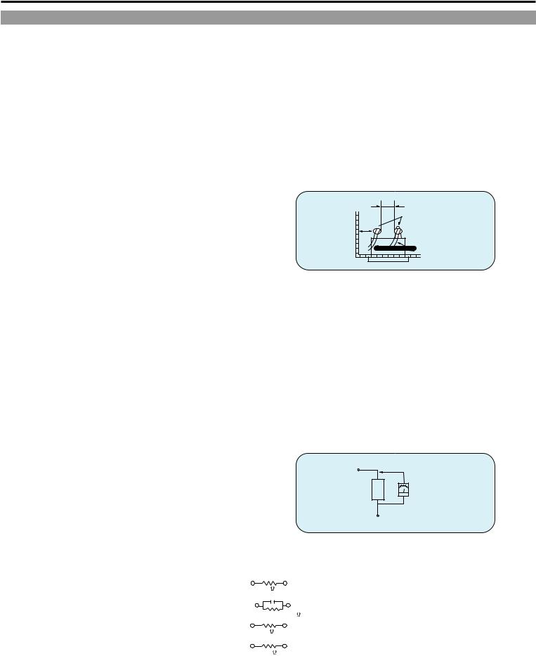
(Standard: 6.5H ± 0.5H)
ADJUSTMENTS 3

2-2. IF MODULE CIRCUIT ADJUSTMENT METHODS
|
|
|
|
|
|
Modulation Method : 30% AM |
|
|
|
|
|
|
|
|
|
|
fm : 400Hz |
|
|
(COMPONENT SIDE) |
|
|
|
fc : 38.9MHz |
|
|
|||
|
|
SIGNAL LEVEL : 80dB V |
|
|
|||||
|
|
|
R191 |
|
|
|
|||
|
|
|
|
SIGNAL |
GEN. |
POWER SUPPLY |
|||
|
|
|
L101 |
|
|
||||
|
|
|
|
|
|
|
|
|
|
9 |
P102 |
1 |
9 |
P101 |
1 |
OUTPUT |
GND |
GND +9V |
+5V |
|
|
|
|
||||||
|
|
|
|
|
|
0.5mS/DIV |
|
|
|
|
|
|
|
|
|
50mV/DIV(10:1) |
|
|
|
|
|
|
|
|
CH1 GND |
|
|
|
|
• ADJUSTMENT PROCEDURE
1)Connect the circuit as above connection diagram.
2)Set the each equipment setting as above description.
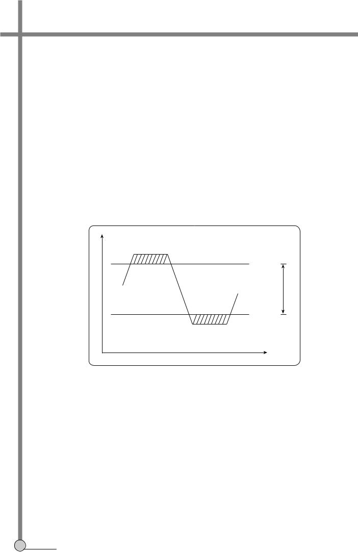
3)Adjust L101 to obtain 2.5 ± 0.15V DC Voltage at check point.
4

2. RF AGC
ADJUSTMENT PARTS |
CHECKING POINT |
TEST EQUIPMENTS |
INPUT SIGNAL |
|
|
|
|
|
|
|
P101 |
Signal Gen. |
|
|
L191 |
Oscilloscope |
Refer to the following. |
||
PIN & |
||||
|
Power Supply |
|
||
|
|
|
||
|
|
|
|
• RF AGC CONNECTION METHOD IF MODULE PCB (TOP VIEW)
|
|
|
|
|
|
Modulation Method : 30% AM |
|
|
|
|
|
|
|
|
|
|
fm : 1KHz |
|
|
(COMPONENT SIDE) |
|
|
|
fc : 38.9MHz |
|
|
|||
|
|
SIGNAL LEVEL : 95dB V |
|
|
|||||
|
|
|
R191 |
|
|
|
|||
|
|
|
|
SIGNAL |
GEN. |
POWER SUPPLY |
|||
|
|
|
L101 |
|
|
||||
|
|
|
|
|
|
|
|
|
|
9 |
P102 |
1 |
9 |
P101 |
1 |
OUTPUT |
GND |
GND +9V |
+5V |
|
|
|
|
||||||
|
|
|
|
|
|
0.5mS/DIV |
|
|
|
|
|
|
+ |
|
|
0.1V/DIV(10:1) |
|
|
|
|
|
|
|
|
|
|
|
|
|
|
2.2 /50V |
|
|
|
|
|
|
||
|
|
|
|
|
CH1 GND |
|
|
|
|
• ADJUSTMENT PROCEDURE
1)Connect the circuit as above connection diagram.
2)Set the each equipment setting as above description.
3)Adjust R191 to obtain 6.0 ± 0.2V DC Voltage at check point.
ADJUSTMENTS 5

SECTION 3. CIRCUIT OPERATION PRINCIPLES
3-1. POWER CIRCUIT
1. OUTLINE
The part that supply DV VOLTAGE to each circuit change AC input voltage into DC voltage. It is based on SMPS(switching mode power supply) system which is located on main PCB. SMPS module is composed of the switching circuit and the transformer of the primary part and the recitifier circuit of the secondary part.
2. NAME AND OPERATION OF PINS ON SMPS MODULE
1) Primary Part
PIN NO |
NAME |
FUNCTION |
|
|
|
|
|
1 |
AC INPUT |
SUPPLY AC INPUT VOLTAGE |
|
|
|||
2 |
|||
|
|
||
|
|
|
|
2) Secondary Part |
|
|
|
|
|
|
|
PIN NO |
NAME |
FUNCTION |
|
|
|
|
|
1 |
+37V |
TURN VOLTAGE OF |
|
TUNER (33V) |
|||
|
|
||
|
|
|
|
2 |
(F+4.5V) |
F/L DISPLAY FILAMENT |
|
VOLTAGE SUPPLY |
|||
|
|
||
|
|
|
|
3 |
(F-GND) |
F/L DISPLAY DRIVE |
|
VOLTAGE SUPPLY |
|||
|
|
||
|
|
|
|
4 |
–27V |
F/L DISPLAY DRIVE |
|
VOLTAGE SUPPLY |
|||
|
|
||
|
|
|
|
5 |
GND |
SECONDARY GND |
|
|
|
|
|
6 |
GND |
SECONDARY GND |
|
|
|
|
|
7 |
GND |
SECONDARY GND |
|
|
|
|
|
8 |
6V |
EVER 5V, ON/OFF 5V |
|
|
|
|
|
9 |
12.4V |
CAP MOT, DRUM MOT (12V) |
|
LOADING MOT (12V) |
|||
|
|
||
|
|
|
6

3. GENERAL CIRCUIT OPERATION
The circuit shown is a highly accurate 37V, 12.4V, 6.0V, -27V, 4.5V, 20W secondary regulated flyback power supply that will operate from 85V to 265 VAC input voltage.
The input voltage is rectified and filtered by D801 and C1. L801, C801, C804 reduce conducted emissin current. C806, L801, C805 reduce common mode noises. R801 is ESD path resistor.
Voltage feedback is obtained from the transformer (T11) bias winding, which eliminates the need for optocoupler and secondary-referenced error amplifier. High-Voltage DC is applied to the primary-high-voltage DC is applied to the primary-winding of T11.
The other side of the transformer primary is driven by the integrated high-voltage MOS FET-transistor within the TOP225(IC11). The circuit operates at a switching frequency of 100KHz, set by the internal oscillator of the TOP (IC11). The clamp circuit impelemented by DZ11, D11, C17 and R13 limits the leading-edge voltage spike caused by transformer leakage inductance to a safe value.
The 37V power secondary winding is rectified by DC1, C25. The 12.4V power secondary winding is rectified and filtered by D24, C24. The 6.0V power secondary winding is rectified and filtered by D23, L22, C23. The -27V power secondary winding is rectified and filtered by DC2 and C22. The F(+) and F(–) power secondary winding is rectified and filtered by DC3, C21 and C29.
A IC21(KA431) shunt regulator directly senses and accurately regulates the output voltage. The effective output voltage can e file turned by adjusting the resistor divider formed by R24, R25 and R26. Other output voltages are possible by adjusting the transformer turns ratio.
The IC21(KA431) regulates the output voltage by controlling optocoupling LED current (and IC11 duty cycle) to maintain an average voltage of 2.5V at the IC21 input pin.
Divider R24, R25 and R26 determine the actual output voltage. C27, R27 rolls off the high frequency gain of the KA31 for stable operation.
R23 limits optocoupler LED current and determines high-frequency loop gain. SPFT start capacitor C26 increases optocoupler current turn-on to limit the duty cycle and down the risting output voltage. C26 has minimal effect on the control loop during normal operation. R22 dicharges soft start capacitor C26 when input power is removed.
The output of the T11 bias winding is rectified and filtered by D12, C11 and R11 to create a typical 12V bias voltage R12, R13 together with the control pin dynamic impedance and capacitor ESR establish a control loop pole-zero pair. C13, R12 also determines the auto frequency and filters internal gate drive switching current.
CIRCUIT 7
3-2. KEY FEATURES OF VIDEO IC AND ITS RELATIVES
1. LA71501BM (QIP 80 PIN): NORMAL AUDIO & Y/C SIGNAL PROCESSING IC
1)Applicable to Multi system (PAL-GBI,MESECAM,3.58NTSC, 4.43NTSC and NAP-GBI)
2)Built-in NAP circuit to convert NTSC to PAL.
3)Normal audio signal processing circuit. (self-alignment for record bias)
4)Buit-in distinction SECAM signal circuit (MESECAM)
5)Built-in Record and Playback FM-EQ function (Switching the specific characteristic is possible by SERIAL CONTROL)
6)Y/C separation using comb filter
7)Built-in Input Switching circuit for 3 Video/Audio input
8)Using serial control by I2 C-BUS
9)Complete Adjustment free
10)Crosstalk reduction by CCD IC for exclusive use (Color Comb filter is unnecessary)
2. LA70001(2CH),LA70011(4CH),LA70020(6CH): PRE-AMP IC
1)AGC circuit is built in this IC (no record current adjustment is required)
2)Built-in the playback signal ENVELOPMENT detection circuit for Auto tracking adjustment.
3. LC89978M: MULTI CCD DELAY LINE IC
1)Built-in Comb Filter for color noise reduction
2)Built-in 1H Delay Line for luminance circuit
3-3. RECORD AND PLAYBACK PROCESSING CIRCUIT
 MICOM 93rd PIN
VIDEO
35 VIDEO AGC SYNC SEP 37
INPUT
|
|
|
|
|
PRE-AMP IC 5th PIN |
|
|
|
|
|
|
|
|
|
|
|
|
FBC |
|
|
LUMINANCE SIGNAL PROCESSING |
||
|
|
||||
|
|
|
CHROMINANCE SIGNAL PROCESSING |
||
|
|
|
|||
FIG.1 Record Processing
The input video signal is then automatically adjusted to suitale level by the built-in VIDEO AGC circuit and supplied to SYNC separation and FBC(feedback clamp) part respectively .
SYNC signal is obtained from the composite video signal ,is supplied to the 93rd pin of MICOM and the
11th pin of PRE-AMP IC to determine the presence of signal ,selection of PAL/NTSC and is using for SERVO control, In PRE-AMP, is using for the HEAD-AMP switching timing and AGC circuit for self-adjustment of the record bias.
The input signal through FBC is processed in luminance signal processing part and chrominance signal processing part independently.
¡ NOTE: Pre-Amp IC varies according to the types of machines. We conform to 4HD’s standard.
8

1)LUMINANCE SIGNAL PROCESSING (RECORD)
FBC |
1/2 |
LPF |
YNR |
25 |
BUFFER |
26 |
CLAMP |
DETAIL |
|
ENHANCER |
|||||||||
|
|
|
|
|
|
|
|
1H DELAY 
 5
5  42
42
7  40
40 
 REC EQ (LC89978M)
PRE-AMP 9th PIN |
|
18 |
|
|
|
|
|
|
|
MAIN |
|
|
N.L. |
|
|
REC EQ |
|
|
FM MOD |
|
|
|
|
||||
|
|
|
|
|
|
EMPHASIS |
|
|
EMPHASIS |
||||
|
|
|
|
|
|
|
|
|
|
|
|
||
|
|
|
|
|
|
|
|
|
|
|
|
|
|
FIG.2 Luminance Signal Processing (RECORD)
FBC |
|
|
|
|
BPF1 |
|
|
ACC |
|
|
|
|
|
|
MAIN |
|
|
C-LPF |
|
|
|
KIL |
|
14 |
|
PRE-AMP 10th PIN |
|
|
|
|
|
|
|
|
|
|
|
|
|
|
|||||||||||||||
|
13 |
|
|
|
|
AMP |
|
|
|
|
|
|
CONV |
|
|
|
|
|
|
|
|
|
|
|
|||
|
|
|
|
|
|
|
|
|
|
|
|
|
|
|
|||||||||||||
|
|
|
|
|
|
|
|
|
|
|
|
|
|
|
|
|
|
|
|
|
|
|
|
|
|||
|
|
|
|
|
|
|
|
|
|
|
|
|
|
|
|
|
|
|
|
|
|
|
|
|
|||
|
|
|
|
|
|
|
|
|
|
|
|
|
|
|
|
|
|
|
|
|
|
|
|
|
|||
|
|
|
|
|
|
|
|
|
|
|
|
|
|
|
|
|
|
|
|
|
|
|
|
||||
|
|
|
|
|
|
|
|
|
|
|
|
|
|
|
|
|
|
|
|
|
|
|
|
|
|
|
|
|
|
|
|
|
|
|
|
|
|
|
|
|
|
|
|
|
|
|
|
|
|
|
|
|
|
|
|
|
|
|
|
|
|
|
|
REC |
|
|
REC |
|
|
|
|
|
|
|
|
|
|
|
|
|
|
||
|
|
|
|
|
|
|
|
|
|
|
|
|
|
|
|
|
|
|
|
|
|
|
|
||||
|
|
|
|
|
|
|
|
DET |
|
|
BGA |
|
|
|
|
|
|
|
|
|
|
|
|
|
|
||
|
|
|
|
|
|
|
|
|
|
|
|
|
|
|
|
|
|
|
|
|
|
|
|
||||
|
|
|
|
|
|
|
|
|
|
|
|
|
|
|
|
|
|
|
|
|
|
|
|
|
|
|
|
FIG.3 Chrominance Signal Processing (RECORD)
CIRCUIT 9
2. PLAYBACK PROCESSING
PRE-AMP |
|
|
35 |
|
|
|
luminance signal |
|
|
|
|
|
|
|
|
|
|
|||||
|
|
|
|
|
processing |
|
|
|
|
|
|
|
|
|
|
|
|
|
|
|||
|
|
|
|
|
|
|
|
|
|
|
|
|
|
|
||||||||
|
|
|
|
|
|
|
|
|
|
|
|
|
|
|
|
|
|
|
|
|||
7th PIN |
|
|
|
|
|
|
|
|
|
|
|
|
|
|
|
|
|
|
|
|
38 |
|
|
|
|
|
|
|
|
|
Y/C MIX |
|
|
FBC |
|
|
VIDEO AMP |
|
|
|
|||||
|
|
|
|
|
|
|
|
|
|
|
|
|
|
|
|
|||||||
|
|
|
|
|
|
|
|
|
|
|
|
|
|
|
|
|
|
|
|
|
||
|
|
|
|
|
|
|
chrominance signal |
|
|
|
|
|
|
|
|
|
|
|
|
|
||
|
|
|
|
|
|
|
|
|
|
|
|
|
|
|
|
|
|
|||||
|
|
|
PB ENVE |
processing |
|
|
|
|
|
|
OSD IC 18th PIN |
|
|
|
|
|||||||
|
|
|
FIG.4 Playback Processing |
|
|
|
|
|||||||||||||||
|
|
|
|
|
|
|
|
|
|
|||||||||||||
|
|
|
|
|
|
|
|
|
|
|
|
|
|
|||||||||
PRE-AMP 7th PIN |
|
|
|
15 |
|
|
|
|
|
|
|
PB-EQ |
|
|
|
17 |
|
|
PHASE COMP |
|
|
|
20 |
|
|
|
|
|
|
FM AGC |
||||||||||||||||||||||||
|
|
|
|
|
|
|
|
|
|
|
|
|
|
|
|
|
||||||||||||||||||||||||||||||||||||||
|
|
|
|
|
|
|
|
|
|
|
|
|
|
|
|
|
|
|
|
|
|
|
|
|
|
|
|
|
|
|
|
|
|
|
|
|
|
|
|
|
|
|
|
|
|
|
|
|
|
|
|
|||
|
|
|
|
|
|
|
|
|
|
|
|
|
|
|
|
|
|
|
|
|
|
|
|
|
|
|
|
|
|
|
|
|
|
|
|
|
|
|
|
|
|
|
|
|
|
|
|
|||||||
|
|
|
|
26 |
|
|
|
|
|
25 |
|
|
|
|
|
|
|
SUB-LPF |
|
|
|
|
FM DEMOD |
|
|
|
|
|
|
DOUBLE LIMITER |
|
|
|
|
|
|
|
|||||||||||||||||
|
|
|
|
|
|
|
|
|
|
|
|
|
|
|
|
|
|
|
|
|
|
|
|
|
|
|||||||||||||||||||||||||||||
|
|
|
|
|
|
|
|
|
|
|
|
|
|
|
|
|
|
|
|
|
|
|
|
|
|
|
|
|
|
|
|
|
|
|
|
|
|
|
|
|
|
|
|
|
|
|
|
|||||||
|
|
|
|
|
|
|
|
|
|
|
|
|
|
|
|
|
|
|
|
|
|
|
|
|
|
|
|
|
|
|
|
|
|
|
|
|
|
|
|
|
|
|
|
|
|
|
|
|
|
|
|
|
|
|
|
|
|
|
|
|
|
|
|
|
|
|
|
|
|
|
|
|
|
|
|
|
|
|
|
|
|
|
|
|
|
|
|
|
|
|
|
|
|
|
|
|
|
|
|||||||||||
CLAMP |
|
|
|
LPF |
|
|
|
|
YNR |
|
|
|
|
|
N.L. DE-EM |
|
|
|
|
DHP NC |
|
|
|
|
PIC CTL |
|
|
|
|
|
Y/C MIX |
|
||||||||||||||||||||||
|
|
|
|
|
|
|
|
|
|
|
|
|
||||||||||||||||||||||||||||||||||||||||||
|
|
|
|
|
|
|
|
|
|
|
|
|
|
|
|
|
|
|
|
|
|
|
|
|
|
|
|
|
|
|
|
|
|
|
|
|
|
|
|
|
|
|
|
|
||||||||||
|
|
|
|
|
|
|
|
|
|
|
|
|
|
|
|
|
|
|
|
|
|
|
|
|
|
|
|
|
|
|
|
|
|
|
|
|||||||||||||||||||
|
|
|
|
|
|
|
|
|
|
|
|
|
|
|
|
|
|
|
|
|
|
|
|
|
|
|
|
|
|
|
|
|
|
|
|
|
|
|
|
|
|
|
|
|
|
|
|
|
|
|
|
|
|
|
|
|
|
|
|
|
|
|
|
|
|
|
42 |
|
|
|
5 |
|
|
|
|
|
|
|
|
|
|
|
|
7 |
|
|
|
40 |
|
|
|
|
|
|
|
|
|
|
|
|
|
|
|
||||||
|
|
|
|
|
|
|
|
|
|
|
|
Y/C MIX |
|
|
|
|
|
|
|
|
|
|
|
CLAMP |
|
|
|
|
||||||||||||||||||||||||||
|
|
|
|
|
|
|
|
|
|
|
|
|
|
|
|
|
|
|
|
|
|
|
|
|
||||||||||||||||||||||||||||||
|
|
|
|
|
|
|
|
|
|
|
|
|
|
|
|
|
|
|
|
|
|
|
|
|
|
|
|
|
|
|
|
|
|
|
|
|
|
|
|
|
|
|
|
|
|
|
|
|
|
|||||
|
|
|
|
|
|
|
|
|
|
|
|
|
|
|
|
|
|
|
|
|
|
|
(LC89978M) |
|
|
|
|
|
|
|
|
|
|
|
|
|
|
|
|
|
|
|
|
|
|
|
|
|
|
|||||
|
|
|
|
|
|
|
|
|
|
|
|
|
|
|
|
|
|
|
|
|
|
|
|
|
|
|||||||||||||||||||||||||||||
|
|
|
|
|
|
|
|
|
|
|
|
FIG.5 Luminance Signal Processing (PB) |
|
|
|
|
|
|
|
|
|
|
|
|
|
|||||||||||||||||||||||||||||
10

2)CHROMINANCE SIGNAL PROCESSING (PB)
PRE-AMP |
15 |
LPF |
|
ACC AMP |
MAIN CONV |
BPF2 |
BPF1 |
7th PIN |
|
||||||
|
|
|
|
|
|
|
|
|
|
|
|
13 |
|
|
|
|
|
|
|
|
|
1 |
50 |
KIL |
LPF |
AMP |
52 |
13 |
+ |
|
|
|
|
|
|
|
2H DELAY |
3 |
48 |
|
|
|
|
|
(LC89978M) |
|
|
NAP |
BPF |
46 |
45 |
CNC |
Y/C MIX |
|
|
FIG.6 Chrominance Signal Processing (PB)
11

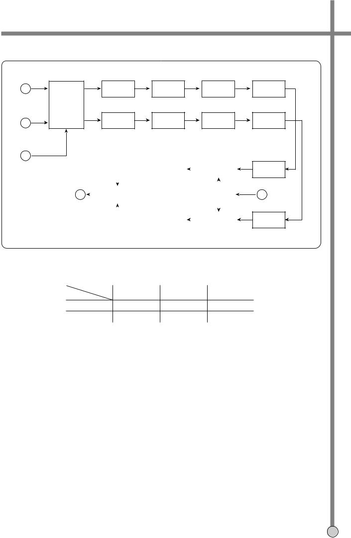
3-4. IF CIRCUIT OPERATION
VCO  AFC
AFC
|
RF |
MIXER |
|
AMP |
|
|
|
|
|
|
LOCAL |
TUNER |
|
OSC |
PRE- |
|
|
SAW |
|
IF |
|
|
VIDEO DET |
|
|
SOUND |
|
|
BUFFER |
|
VIDEO |
AMP |
|
|
FILTER |
|
AMP |
|
|
& DEMOD |
|
|
TRAP |
|
|
|
OUT |
|
|
|
|
|
|
|
|
|
|
|
|
||||||
|
|
|
|
|
|
|
|
|
|
|
|
|
|
|
|
|
AGC
DET
-COM
The signal from the ANT is amplified for selectivity, to decrease image interference, and increase S/N using the RF AMP. The RF signal at the MIXER is subtracted from the LOCAL OSC frequency using the upperside band method, to change is into the IF signal; 38.9MHz. The IF signal converted from the RF signal in the tuner block is amplified by about 28dB to increase S/N in the pre-amp block. The reason for thesis that the SAW filter has its own insertion loss of about-18 to -22dB. The SAW filter is a kind of BPF, used to remove the near channel harmonics and make the desired frequency response. The IF AMP desired of about 60 to 70dB gain for receiver sensitivity and selectivity. The vision IF AMP consists of three AC-coupled differential amplifier stages; each stage uses a controlled feedback network called AGC. To maintain the video output signal at a constant level the automatic control voltage is generated according to the transmission standard. For negative modulation in the PAL standard the peak-sync level is detected. The AGC detector charges and discharges the AGC capacitor to set the IF gain and the tuner gain. We can also adjust the tuner AGC voltage take over point. This allow the tuner and the IF SAW filter to be matched to achieve the optimum IF input signal. The IF amplifier output signal is fed to a frequency detector and to a phase detector. The frequency detector is operational before lock-in. A DC current is generated which is proportional to the frequency difference between the input signal and the VCO frequency. The control voltage for the VCO is provided by the phase detector. The demodulate output signal is fed via an integrated LPF (about 12MHz) to the video amplifier for suppression of the carrier harmonics.
The VCO operates with a symmetrically-connected reference L-C circuit, running at the double vision carrier frequency (77.8MHz) to decrease the frequency error. Fequency control is performed by an internal varicap diode. The voltage used to set the VCO frequency to the actual double vision carrier frequency, is also amplified and converted to give the AFC output current. The AFC output is fed to the µ-COM to change the LOCAL OSC frequency and for channel searching. The VCO signal is divided by-two in a travelling wave divider, which generates two differenctial output signals with exactly 90 degrees phase difference, independent of frequency. The video signal passing through the 5.5MHz sound trap is fed to the buffer.
12
2. PAL AUDIO FLOW (Two carrier) (Hi-Fi only model)
VIDEO DET |
intercarrier |
|
SOUND |
|
|
LIMITER |
||
& DEMOD |
|
|
|
|
BPF |
|
|
AMP |
|
|
|
|
|
|
|
|
|
|
|
|
|
|
VIDEO BLOCK |
|||
|
|
|
|
|
||||
FM PLL-
DEMOD.
FM PLL- |
DEMOD. |
AF |
|
AUDIO OUT (L) |
|
||
AMP |
|
AUDIO OUT (R) |
|
||
|
|
|
DIGITAL  STEREO(LOW) INTEGRATOR
  DUAL(LOW)
13
4. TM BLOCK
The TUNER and MODULATOR which is separated to each module conventionally, is presently united to one block (TM block)
(a)PLL METHOD AND I2C-BUS CONTROL
The RF OUTPUT channel can be varied from 22CH to 69CH by remote control using PLL method and I2C-BUS control.
Moreover, SYSTEM(PAL, MESECAM, NTSC), SOUND CARRIER FREQUENCY, AND TPSG(TEST PATTERN SIGNAL GENERATOR) can be changed by remote conrol as well.
The P/S ration, white clip, power saving, etc., also can be controlled only by changing a I2C-BUS data according to the designer‘s intention.
(b)DIGITAL AFT METHOD
Conventionally, when the frequency deviates, the variation of AFT output from IF circuit was compensated by feedbacking it to TUNER AFT input.
On the other hand, if AFT, which is currently adopted to these models from IF circuit deviates the window range, the VT value is changed to maintain the AFT voltage to be within window range by checking AFT(+) and AFT(–) on MICOM.
VOLTAGE |
AFT(+) |
3V |
WINDOW |
2V |
AFT(–) |
FREQ. |
14

3-5. NORMAL AUDIO SIGNAL PROCESSING(LA71501BM)
The circuitry of Normal AUDIO part is similar to that of the conventional Normal AUDIO part in case of EE and PB mode, but in REC mode, due to the internal opeation of self-alignment, it shows a lot of differences.
1. EE MODE
LA71501BM has 3-input VIDEO/AUDIO switching circuitry internally, and its switching is controlled by the serial data dispatched from MICOM.
In the case of Hi-Fi models, only One input is used. The Normal AUDIO signal from Hi-Fi Audio part is divided by the resistor, R202 and R203 and then supplied to the 73rd pin of LA71501BM. Its level is automatically controlled by ALC and then the amplified signal through LINE AMP is obtained at the 77th pin.
The signal from C208 is supplied to REC AMP after the divider circuit (R204, R205, R207) and also to the Hi-Fi IC BH7804K.
The ALC point can be adjusted by R208 and R209, the adjustment of which is closely related to the REC level in REC mode.
The ALC time can be adjusted by R201 and C201.
At the MONO model, 3 input VIDEO/AUDIO switching circuit (Internal IC) is fully used. IF audio signal is supplied to pin 71, AV signal to pin 73. Additionally F/AV signal is not used. Afterwards, Mono model is the two input system.
2. PB MODE
The PB signal picked up from AUDIO HEAD is firstly processed in the frequency characteristic compensator which is composed of R220 and C214 (EP: C214+C215) and then supplied to the 7th pin.
The input signal passes through EQ AMP, and LINE AMP, so its output signal is finally obtained from the 77th pin. The circuitry and its operation of EQ AMP is identical to the conventional EQ AMP.
3. REC MODE
1)AUDIO SWITCHING CIRCUIT
When the AUDIO S/W signal at the 80th pin is “H”, the point at the AUDIO HEAD of the external switching circuit is opened electrically (EE/PB=GND), so the COIL starts to oscillated.
|
REC: OPEN |
VCC |
|
R218 |
R215 |
|
|
EE: GND |
|
||
5 |
Q203 |
R216 |
|
BIAS COIL |
|
||
|
|
||
|
R214 |
|
|
5th PIN |
|
A-H |
|
|
|
80 |
|
R/P |
|
S/W |
|
HEAD |
|
Q202 |
|
|
R217 |
|
|
|
|
|
|
|
Q204 |
|
|
External Switching Circuit
CIRCUIT 15

3)The output AUDIO signal at the 1st pin through REC AMP is recorded on HEAD after being mixed with the 70KHz AC BIAS signal.
At the same time, the output AUDIO signal is supplied to the 3rd pin and then filtered by 60KHz HPF, so only the 70KHz AC BIAS signal is passed.
The pure 70KHz AC BIAS signal is then compared to the voltage of 440mV at the comparator, so the AC BIAS signal is controlled to maintain at 440mV.
4)The recording current is determined by the 440mVrms BIAS signal and the resistance between the 1st and the 3rd
pin.
* The method to set the recording current.
BIAS=440mVrms ÷ the resistance between the 1st and the 3rd pin. ex) 440mVrms ÷ 1.8K OHM = 244µA
where, only the low error, G type resistor should be used here.
As a rule of thumb, the resistance between the 1st and the 3rd pin should range from 1.0 ohm to 2.2K ohm.
5)The conventional AUDIO circuitry uses a peaking COIL to enhance the high frequency region, but the LA71511M uses the resistance of R/P HEAD.
Accordingly, The resistor and the capacitor is used to fit the frequency characteristics.
4. BIAS COIL
For normal operation of AUTO BIAS, the oscillating voltage of R/P HEAD is over 40Vp-p, A/E HEAD is over 20Vp-p, and the FE HEAD is over 40Vp-p.
Especially, the erasing current of F/E HEAD ranges from 130 to 280mA, and it should be 180mA when the HEAD impedance is at the center.
3-6. HI-FI AUDIO SIGNAL PROCESSING (BH7804K)
1. SPECIAL FEATURES
BH7804K processes the conventional Hi-Fi audio and additionally, contains special parts as the below.
(1)As ± 2 power source formula is adapted, decrease of coupling capacitor is possible the REGULATOR circuit is built in.
(2)Built in I2C bus control decoder circuit which has two lines formula, each mode for the inside of IC is set up by serial data.
(3)Reverse characteristics system during recording and playback are used in both the PNR (Peak Noise Reduction) processor and FM MODEM. And it can be simultaneous adjustment of carrier frequency and FM deviation/playback level. And it can be independent adjustment of FM deviation/playback level. (The adjustment of Lch and Rch is simultaneous.)
(4)Slope control FM switching noise correction circuit is built in.
(5)Auto adjust circuit of VCO and BPF making use of Fsc (3.58MHz) is built in. It is possible to adjust changelessly without drift by board mounting stress and time.
16
2. REC MODE
L |
LPF |
PNR |
FM |
|
EMPH |
||||
|
|
|
||
|
INPUT |
|
|
|
|
SW |
|
FM |
|
R |
LPF |
PNR |
||
EMPH |
||||
|
|
31
|
|
|
|
|
|
REC FM |
|
|
1.4M |
|
|
|
|
|
|
|
LPF |
|
|
MOD |
|
|
|
|
|
|
|
|
|
|
|
|
|
|
|
|
|
|
|
|
|
|
|
REC FM OUT |
21 |
|
FM |
|
|
|
AUTO |
|||
|
MIX |
|
|
|
|
ADJ |
||||
|
|
|
|
|
|
|||||
|
|
|
|
|
|
|
|
|
|
|
|
|
|
|
|
|
|
|
|
|
|
|
|
|
|
|
|
REC FM |
|
|
1.8M |
|
|
|
|
|
|
|
LPF |
|
|
MOD |
|
INPUT |
IF |
AV |
F.AV |
|
CH |
||||
|
|
|
||
L |
2 |
41 |
34 |
|
R |
1 |
40 |
33 |
|
|
|
|
|
LPF
LPF
AUDIO
LIM
8 Fsc
AUDIO
LIM
CIRCUIT 17
3. PB MODE
|
|
|
|
|
|
|
|
|
|
|
|
|
|
|
|
|
|
|
LPF |
|
|
FM |
|
|
|
|
DEMOD |
|
|
|
SW NOISE |
||||||||||||
|
|
|
|
|
|
|
|
|
|
|
|
|
|
|
|
|
|
|
|
|
LIM |
|
|
|
|
|
|
|
COMPEN |
||||||||||||||
|
|
|
|
|
|
|
|
|
|
|
|
|
|
|
|
|
|
|
|
|
|
|
|
|
|
|
|
|
|
|
|
|
|
|
|
|
|
||||||
FM PB IN |
AMP |
|
|
|
|
|
|
|
|
|
|
|
|
|
|
|
|
|
|
|
|
|
|
|
|
|
|
|
|
|
|
|
|
|
|||||||||
|
|
|
|
|
|
|
|
|
|
|
|
|
|
|
|
|
|
|
|
|
|
|
|
|
|
|
|
|
|
|
|
|
|||||||||||
13 |
|
|
|
|
|
|
|
|
|
|
|
|
|
|
|
|
|
|
|
|
|
|
|
|
|
|
|
|
|
|
|
|
|
|
|
|
|
|
|||||
|
|
|
|
|
|
|
|
|
|
|
|
|
|
|
|
|
|
|
|
|
|
|
|
|
|
|
|
|
|
|
|
|
|
|
|
|
|
|
|||||
|
|
|
|
|
|
|
|
|
|
|
|
|
|
|
|
|
D.O. |
|
|
|
HOLD |
|
|
|
|
|
|
|
|
|
|
||||||||||||
|
|
|
|
|
|
|
|
|
|
|
|
|
|
|
|
|
|
|
|
|
|
|
|
|
|
|
|
8 |
|
A SW |
|
||||||||||||
|
|
|
|
|
|
|
|
|
|
|
|
|
|
|
|
|
|
|
|
|
|
DET |
|
|
PULSE GEN |
|
|
|
|
|
|||||||||||||
|
|
|
|
|
|
|
|
|
|
|
|
|
|
|
|
|
|
|
|
|
|
|
|
|
|
|
PULSE |
|
|||||||||||||||
|
|
|
|
|
|
|
|
|
|
|
|
|
|
|
|
|
|
|
|
|
|
|
|
|
|
|
|
|
|
|
|
|
|
|
|
|
|
||||||
|
|
|
|
|
|
|
|
|
|
|
|
|
|
|
|
|
|
|
|
|
|
|
|
|
|
|
|
|
|
|
|
|
|
|
|
|
|
|
|
|
|||
|
|
|
|
|
|
|
|
|
|
|
|
|
|
|
|
|
|
|
|
|
|
|
|
|
|
|
|
|
|
|
|
|
|
|
|
|
|
|
|
|
|||
|
|
|
|
|
|
|
|
|
|
|
|
|
|
|
|
|
|
|
|
|
|
|
|
|
|
|
|
|
|
|
|
|
|
|
|
|
|
|
|
|
|
|
|
|
|
|
|
|
|
|
|
FM |
|
|
|
|
|
|
LPF |
|
|
|
|
|
FM |
|
|
|
|
DEMOD |
|
|
|
SW NOISE |
|||||||||||||
|
|
|
|
|
|
|
|
ALC |
|
|
|
|
|
|
|
|
|
|
|
|
|
|
LIM |
|
|
|
|
|
|
|
COMPEN |
||||||||||||
|
|
|
|
|
|
|
|
|
|
|
|
|
|
|
|
|
|
|
|
|
|
|
|
|
|
|
|
|
|
||||||||||||||
Hi-Fi DET |
|
|
|
|
|
|
|
|
|
|
|
|
|
|
|
|
|
|
|
|
|
|
|
|
|
|
|
|
|
|
|
|
|
|
|
|
|
|
|||||
|
|
ENVE/ |
|
|
|
|
|
|
|
|
|
|
|
|
|
|
|
|
|
|
|
|
|
|
|
|
|
|
|
|
|
|
|
|
|
|
|||||||
14 |
|
|
|
|
|
|
|
|
|
|
|
|
|
|
|
|
|
|
|
|
|
|
|
|
|
|
|
|
|
|
FM |
|
|
|
|
|
|
||||||
|
|
|
|
|
|
|
|
|
|
|
|
|
|
|
|
|
|
|
|
|
|
|
|
|
|
|
|
|
|
||||||||||||||
|
|
|
|
|
|
|
HiFi |
|
|
|
|
|
|
|
|
|
|
|
|
|
|
|
|
|
|
|
|
|
|
|
|
|
|
|
|
|
|
||||||
|
|
|
|
|
|
|
|
|
|
|
|
|
|
|
|
|
|
|
|
|
|
|
|
|
|
|
DET |
|
|
|
|
|
|
||||||||||
AUDIO OUT(L) |
|
|
|
|
|
|
|
|
|
|
|
|
|
|
|
|
|
|
|
|
|
|
|
|
|
|
|
|
|
|
|
|
|
||||||||||
|
|
|
|
|
|
|
|
|
|
|
|
|
|
|
|
|
|
|
|
|
|
|
|
|
|
|
|
|
|
|
|
|
|
|
|
|
|||||||
30 |
|
|
|
|
|
|
|
|
AMP |
|
|
|
|
|
|
|
|
PNR |
|
|
|
|
|
FM |
|
|
|
LPF |
|||||||||||||||
|
|
|
|
|
|
|
|
|
|
OUTPUT |
|
|
|
|
|
|
|
DE-EMPH |
|
|
|
||||||||||||||||||||||
MOD OUT 27 |
|
|
|
|
|
|
|
|
|
|
|
|
|
|
|
|
|
|
|
|
|
|
|
|
|
|
|
|
|
|
|
|
|
||||||||||
|
|
|
|
|
|
|
|
|
|
|
|
|
|
|
|
|
|
|
|
|
|
|
|
|
|
|
|
|
|
|
|
|
|
|
|
|
|||||||
|
|
|
|
|
|
|
|
|
|
|
|
|
|
|
SW |
|
|
|
|
|
|
|
|
|
|
|
|
|
|
|
|
|
|
|
|
|
|||||||
29 |
|
|
|
|
|
|
|
|
AMP |
|
|
|
|
PNR |
|
|
|
|
|
FM |
|
|
|
LPF |
|||||||||||||||||||
|
|
|
|
|
|
|
|
|
|
|
|
|
|
|
|
|
|
|
|
|
|
|
|||||||||||||||||||||
|
|
|
|
|
|
|
|
|
|
|
|
|
|
|
|
|
|
|
DE-EMPH |
|
|
|
|||||||||||||||||||||
AUDIO OUT(R) |
|
|
|
|
|
|
|
|
|
|
|
|
|
|
|
|
|
|
|
|
|
|
|
|
|
|
|
|
|
|
|
|
|||||||||||
|
|
|
|
|
|
|
|
|
|
|
|
|
|
|
|
|
|
|
|
|
|
|
|
|
|
|
|
|
|
|
|
|
|
|
|
|
|||||||
|
|
|
|
NORMAL AUDIO 26 |
|
|
|
|
|
|
|
|
|
|
|
|
|
|
|
|
|
|
|
|
|
|
|
|
|
||||||||||||||
|
|
|
|
|
|
|
|
|
|
|
|
|
|
|
|
|
|
|
|
|
|
|
|
|
|
|
|
|
|||||||||||||||
-
18
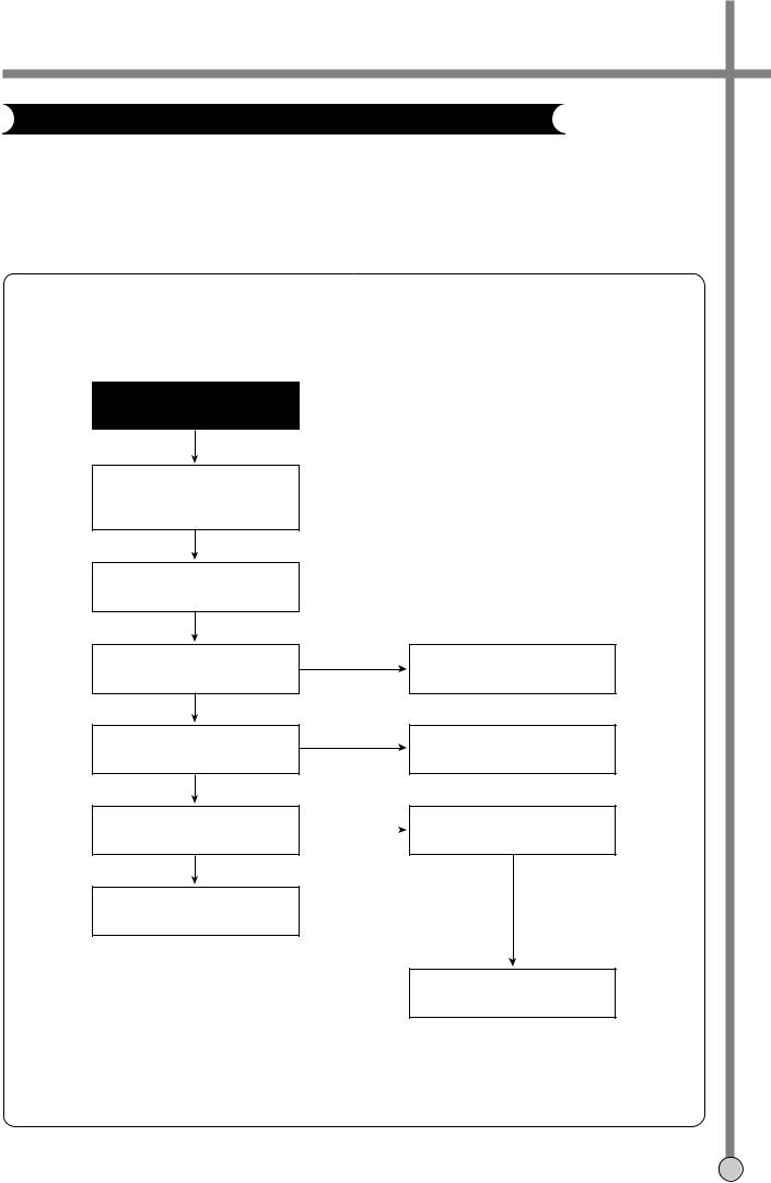
SECTION 4. TROUBLESHOOTING FLOW CHART
4-1. POWER CIRCUIT
When changing the parts which are broken first, remove the power plug from the socket and then discharge the voltage across the terminals of C807 (use an external 1KΩ (2W) resistance).
When check the primary circuit, Use the oscilloscope isolated properly (Use the isolated transformer) and connect GND to the primary GND, however it is not necessary to isolate the oscilloscope when check the secondary circuit.
A. CHECKING THE PRIMARY CIRCUIT.
No output Voltage.
YES
Prepare the oscilloscope connected the isolated transformer
YES
Check F801 Fuse.
YES
Is voltage applied to D801?
YES
Is voltage applied to the terminals of C807?
YES
Is 5.7 voltage applied to IC11 control pin
YES
Check the secondary circuit
NO
Check L801, L802
NO
Check R803, D801
NO |
Is varation between 5.7V |
and 4.8V at IC11 control pin
NO
Check T11 : #~^ pin,
L12 and IC11
FLOW CHART 19

B. CHECKING THE SECONDARY CIRCUIT
NO
Check each output voltage
YES
YES
Check the CN21
END
Check transformer of NO output stages
YES
Check the diode of NO output stages
YES
Check the COIL, C of NO
output stages
20

4-2. PIF CIRCUIT TROUBLESHOOTING
A. TROUBLESHOOTING OF RF RECEIVING CIRCUIT
Is Video Signal Video Out point, |
|
YES |
|
|
Check the A/V Switching and |
|||||
|
|
|
|
|||||||
|
P101 Pin No. 4 of IF Module? |
|
|
|
|
Video Circduit. |
||||
|
|
|
||||||||
|
|
|
|
|
|
|
|
|
|
|
|
|
|
|
NO |
|
|
|
|
|
|
|
|
|
|
YES |
|
|
|
|||
Is Audio signal at Audio Out point, |
|
|
|
|
||||||
P102 Pin No.2/No. 4 of IF Module? |
|
|
|
|
|
|||||
|
|
|
|
|
|
|
|
|
|
|
|
|
|
|
NO |
|
|
|
|
|
|
|
|
|
NO |
|
|
|
||||
|
Is +5V supplied to BB point, |
|
|
|
Check the Power Supply Circuit. |
|||||
|
|
Pin No. 1 of TM Block? |
|
|
|
|
||||
|
|
|
|
|
|
|
||||
|
|
|
|
|
|
|
|
|
|
|
|
|
|
|
YES |
|
|
|
|
|
|
|
|
|
NO |
|
|
|
||||
|
Is +9V supplied to IF 9V point, |
|
|
|
Check Q179, Q180 and Power |
|||||
|
P101 Pin No. 3 of IF Module? |
|
|
|
|
Supply Circuit. |
||||
|
|
|
|
|
|
|
|
|
|
|
|
|
|
|
YES |
|
|
|
|
|
|
|
|
|
|
|
NO |
|
|
|
||
|
|
|
|
|
|
|||||
|
Is +5V supplied to IF 5V point, |
|
|
|
Check Q177, Q178 and Power |
|||||
|
P102 Pin No. 5 of IF Module? |
|
|
|
|
Supply circuit. |
||||
|
|
|
|
|
|
|
|
|
|
|
|
YES |
|
YES |
ƒk |
|
ƒk |
|
|||
|
|
NO |
Check NTSC(H) port of -COM |
|||||||
|
|
|
|
|
||||||
|
|
|
Is NTSC(H) Supplied to p102 |
|
|
|||||
|
|
|
|
|
Pin No. 100 and Q103, Q104, |
|||||
|
|
|
Pin No. 8 of IF Model? |
|
|
|
Q105, Q106, Q107, Q108, Q109, |
|||
|
|
|
|
|
|
|
|
|
|
Q110, Q111, Q113 of IF Module |
|
|
|
|
YES |
|
|
NO |
|
|
|
|
|
|
|
|
|
|
|
|
||
|
|
|
|
|
|
|
|
|
||
|
|
|
|
|
|
|||||
|
Is tunning voltage changed |
|
|
|
Check Q181 EVER 33V and then |
|||||
|
when changing channels? |
|
|
|
|
PWM from -COM. |
||||
|
|
|
|
|
|
|
|
|
|
|
YES
Is +9V supplied to VL, VH or U band point, Pin No. 15, 16 or 17 or TM Block?
YES
Is RF AGC adjusted well?
YES
Is AFT adjusted well?
YES
Change the IF Module and then TM Block.
NO |
|
Check the transistors from Q171 to |
|
Q176 and -COM ports, VL(H), |
|
|
|
|
|
|
VH(H) and UHF(H) |
|
|
|
NO
Correct RF AGC adjustment.
NO
Correct AFT adjustment.
¡ NOTE: ƒk means when NTSC signal received.
FLOW CHART 21

B. TROUBLESHOOTING OF RF MODULATOR OUT
Is Video Signal Video In point, |
|
NO |
|
|
|
|
|
||
Pin No. 6 of TM Block? |
|
|
|
|
|
|
|
||
|
|
|
|
|
|
YES |
|
|
|
|
|
|
NO |
|
|
|
|
||
Is Audio signal at Audio In point, |
|
|
||
Pin No.2 of TM Block? |
|
|
|
|
|
|
|
|
|
|
YES |
|
|
|
|
|
NO |
|
|
Are RF OUT System and RF Out |
|
|
||
channel selected well by menu key. |
|
|
|
|
|
|
|
|
|
|
YES |
|
|
|
|
|
|
|
|
Is system Select Option Diode |
|
NO |
|
|
applied well according to Option |
|
|
|
|
|
|
|
||
Table? |
|
|
|
|
|
|
|
|
|
|
YES |
|
|
|
|
|
|
NO |
|
|
|
|
||
Is +5V supplied to MB point, |
|
|
||
Pin No. 4 of TM Block? |
|
|
|
|
|
|
|
|
|
|
YES |
|
|
|
|
|
NO |
|
|
Is +30V supplied to TU(MD) point, |
|
|
||
Pin No. 7 of TM Block? |
|
|
|
|
|
|
|
|
|
|
YES |
|
|
|
|
|
|
|
|
Is Serial Data supplied to |
|
NO |
|
|
SDA points, Pin No. 3 of |
|
|
||
|
|
|
||
TM Block? |
|
|
|
|
|
|
|
|
|
|
YES |
|
|
|
|
|
|
|
|
Is Serial Clock supplied to |
|
NO |
|
|
SCL points, Pin No. 5 of |
|
|
||
|
|
|
||
TM Block? |
|
|
|
|
|
|
|
|
|
|
YES |
|
|
|
|
|
|
|
|
Change the TM Block. |
|
|
|
|
|
|
|
|
|
Check the A/V Switching, Video
and Audio Circduit.
Select the RIGHT System and
channel by menu key.
Correct the Option.
Check on/off 5V and Power Supply circuit.
Check D171 and Power
Supply circuit.
Check the -COM port, SDA.
Check the -COM port, SCL.
22

4-3. LOGIC CIRCUIT
A.
Digitron does not operate.
YES
Is +5V supplied to pin c of IC501?
YES
Is 24V supplied to pin C of IC501?
YES
Are -20 and -16.5V supplied to pin e and ! of G701?
YES
Check IC501
and change.
B.
Digitron is lit keys do not operate.
Is each key pulse applied to pin Gg H and h of IC501?
YES
Check the pin serial of pin A,a of IC501
Is +5.8V supplied |
NO |
|
Check power Module |
fdrom D509 cathod? |
|
|
|
|
|
|
|
|
|
|
|
Check power
Module
Check power
Module
Check power
Module
Check key matrix circuit.
FLOW CHART 23
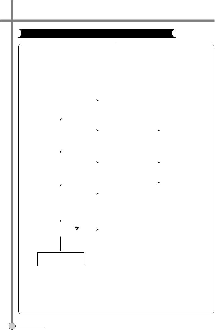
4-4. SERVO-SYSCON CIRCUIT
A.
Playback picture |
|
|
Adjust tracking. |
|
is not good |
|
|
||
|
|
|
||
|
|
|
|
|
|
|
|
|
|
Noise appears |
NO |
|
Noise appears |
YES |
Check and re-adjust |
|||
although |
|
although |
||||||
|
|
|
|
|||||
|
|
|
|
the path of Deck. |
||||
adjusting tracking. |
|
|
change cassette tape. |
|
|
|||
|
|
|
|
|
||||
|
|
|
|
|
|
|
|
|
|
YES |
|
|
|
|
|
|
|
|
|
|
|
|
|
|
|
|
|
|
|
|
|
|
|
|
|
Is CTL pulse output |
NO |
|
CTL HEAD height |
NO |
Adjust the HEAD |
|||
|
is normal and |
height and |
||||||
at pin ^ of IC505? |
|
|
|
|
||||
|
|
there is not dust? |
|
|
remove dust. |
|||
|
|
|
|
|
|
|||
|
|
|
|
|
|
|
|
|
|
YES |
|
|
|
|
YES |
|
|
|
|
|
|
|
Check circuit |
|||
|
|
NO |
|
|
|
|
|
adjacent to IC505 |
|
|
|
|
|
|
|
||
IsPlaybackCTL pulsepictureinput |
|
Check R528, R527, |
|
|
|
|||
|
|
|
|
|||||
to pinis QnotofgoodIC501? |
|
|
R529, R523 |
|
|
|
||
|
|
|
|
|
|
|
|
|
|
YES |
|
|
|
|
|
|
|
|
|
NO |
|
|
|
|
|
|
|
|
|
|
|
|
|
|
|
The voltage of pin |
|
Check R551, C532 |
|
|
|
|||
of IC501 not changing? |
|
|
|
|
|
|||
|
|
|
|
|
|
|
||
|
|
|
|
|
|
|
|
|
YES
Playback picture Check IC501 is not good
24

B.
Playback picture is not good.
Noise appears on the |
NO |
|
|
screen on the whole. |
|
|
|
YES
Are SW-pulse and HA-SW NO
applied to preamp circuit?
|
YES |
|
|
|
|
|
|
|
Is Enve. waveform |
NO |
|
supplied to pin % of |
|
|
|
||
PT01? |
|
|
|
|
|
YES
Check video circuit.
Noise appears on the |
NO |
|
|
||
screen at the bottom |
|
|
|
|
YES |
|
|
|
|
|
|
Is sw pulse supplied NO from pin 8 of IC501?
YES
Check connector, |
NO |
Head Amp |
|
|
|
and Head dust. |
|
|
|
Check flow A.
Adjust the PG
in SVC mode.
Check D.PG input and connector.
Check pattern
Change Drum Ass'y
FLOW CHART 25
C.
Auto-stop during playback.
Is reel pulse applied to pin % and ^of IC501?
YES
Is D. FG applied to pin = of IC501?
YES
Check IC501.
NO
Check reel sensor.
NO |
|
Check connector and |
|
|
D. FG circuits. |
|
|
|
26

D.
Drum M/T loading stops.
Is motor 12V supplied to IC502 & *pin 12V?
YES
Is 6V supplied to pin $ of IC502?
YES
Change IC502
YES
Check connector and motor.
NO
Check Q504.
NO
Check power module.
NO
Check Q504.
NO |
|
Check P503 and |
|
|
|
|
|
Loading motor |
|
|
|
FLOW CHART 27
 Loading...