


CONTENTS
CONTENTS |
|
SPECIFICATIONS......................................................................................................................... |
2 |
CIRCUIT OPERATIONAL DESCRIPTION......................................................................................... |
3 |
VOLTAGE CHARTS..................................................................................................................... |
18 |
CIRCUIT DIAGRAM................................................................................................................... |
19 |
PCB CIRCUIT BOARD................................................................................................................. |
29 |
WAVEFORMS............................................................................................................................ |
40 |
TROUBLE SHOOTING................................................................................................................. |
47 |
INSTRUMENT DISASSEMBLY...................................................................................................... |
53 |
PARTLIST................................................................................................................................... |
61 |
Sm(DAEWOO_1389C)060109.indd |
1 |
|
|
2006-1-13 |
15:51:21 |
|
|
||||
|
|
|
|
|
|
|
|
|
|
|
|

SPECIFICATIONS
|
|
|
Laser |
wavelength 650nm |
|
|
|
|
|
|
|
|
|
|
Video |
PAL/AUTO/NTSC |
|
|
|
|
|
|
|
|
Frequency response |
20Hz ~ 20KHz (±1dB) |
|||
|
|
|
|
|
|
|
Signal/noise ratio |
≥90dB |
|||
|
|
|
|
|
|
|
Channel separation |
≥85dB ( 1KHz) |
|||
|
|
|
|
|
|
|
Dynamic range |
≥80dB ( 1KHz) |
|||
|
|
|
|
|
|
|
|
|
|
Analog |
output level : 2.0 + 0/-0.2Vrms |
Output |
|
|
|
(Load impedance : 1,0KΩ) |
|
|
|
|
|
||
Audio |
|
|
|
Digital |
output level : 0.5 ±0.1Vp-p |
|
|
|
|
||
|
|
|
|
(Load impedance : 75Ω) |
|
|
|
|
|
|
|
|
|
|
|
|
|
|
|
|
|
Composite |
output level : 1.0 ±0.1Vp-p |
|
|
|
|
(Load impedance : 75Ω, imbalance, negative polarity) |
|
|
|
|
|
|
|
Output |
|
|
|
|
|
|
|
|
|
output level : brightness(Luma) 1.0 ±0.1Vp-p Chromaticity (Color) |
|
Video |
|
|
|
S-video |
0.286 ±20% |
|
|
|
|
|
(Load impedance : 75Ω) |
|
|
|
|
|
|
|
|
|
|
Component |
Y: 1Vp-p, Pb/Pr: 0.7Vp-p (Load impedance : 75Ω) |
|
|
|
Power |
100-240V~, 50Hz~60Hz 12W |
|
|
|
|
|
|
|
Dimensiones |
|
Body (W x H x D) |
430 x 38 x 245 mm |
||
|
|
|
|||
|
Packing |
510 x 88 x 305 mm |
|||
|
|
|
|
||
|
|
|
|
||
|
Weight (Gross / Net) |
2.9Kg / 2.2Kg |
|||
|
|
|
|
|
|
Notes : Design and specifications in this instruction manual are subjected to change without prior notice toimprove quality and function.
 DVD Audio output standards
Output |
|
Disc type |
|
|
DVD |
VIDEO-CD |
CD |
||
|
||||
Analogue Audio output |
48/96KHz sampling |
44.1KHz sampling |
44.1KHz sampling |
|
Digital Audio output |
48KHz sampling |
44.1KHz sampling |
44.1KHz sampling |
Sm(DAEWOO_1389C)060109.indd |
2 |
|
|
2006-1-13 |
15:41:56 |
|
|
||||
|
|
|
|
|
|
|
|
|
|
|
|
CIRCUIT OPERATIONAL DESCRIPTION
DVD Module
1. Summary
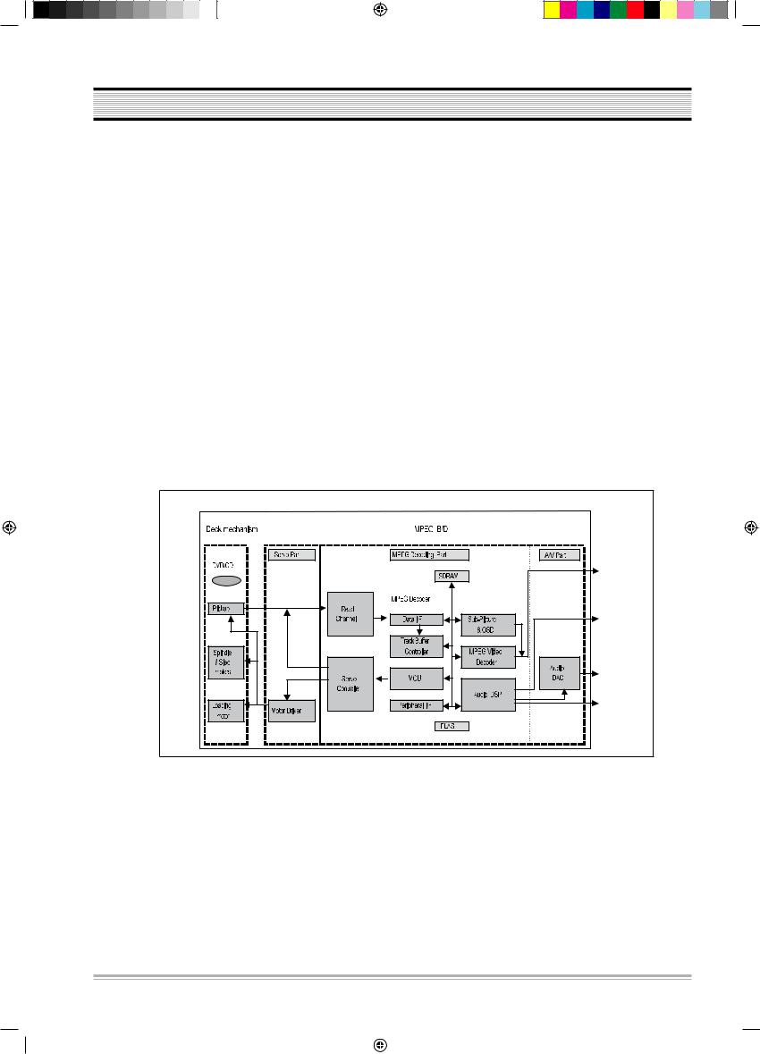
DVD One Board consists of: Loader part that reads and transmits audio and video data saved at Optic Discs (DVD, CD-DA, VCD, CD-R) to MPEG Decoder part; MPEG Decoder part, which, by decoding and encoding data received from the Loader, produces analog signals; and u-Com that controls the overall system including the loader and MPEG decoder.
2. How Does it Operate
Insert the power cord and then power transmitted to each IC, and the SET will be the STANDBY status which requires the least power for input the front panel key, input the STAND BY/ ON key, extinguished the LED. Once the Power On key is entered, u-Com recognizes it and initiates each chipset, performs sequential algorithms such as determining whether the disc is in or not, and if in, what type of disc is loaded.
Through this process, it can read disc data before transmitting it to the MPEG Decoder. The MPEG Decoder will then decode and encode such data before generating the final analog audio and video signal outputs.
DVD-MODULE Block Diagram
Sm(DAEWOO_1389C)060109.indd |
3 |
|
|
2006-1-13 |
15:41:57 |
|
|
||||
|
|
|
|
|
|
|
|
|
|
|
|
CIRCUIT OPERATIONAL DESCRIPTION
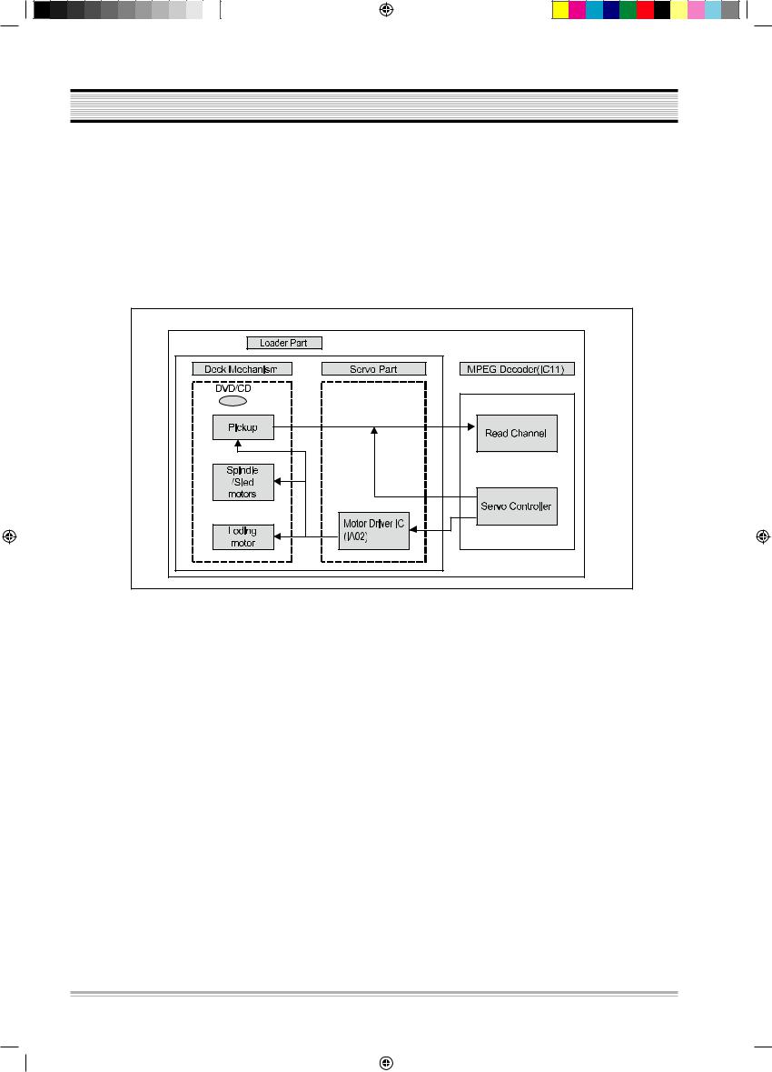
3. Loader Part
The loader which read the data of audio/video from optic disc and transfer them to MPEG decoder can be divided into Deck total DVD assay(in a short term, Mecha) and Servo. Mecha mounts with the optical pick-up which allows reading the signal of a disc using laser beam and makes it operates and consists of the deck mechanism which allows loading a disc and reading the data. Servo is a sort of circuit which allows operating the loader and recovering the data and consists of Motor Drive IC operating the spindle, the sled, the loading motor.
Loader Block Diagram
Sm(DAEWOO_1389C)060109.indd |
4 |
|
|
2006-1-13 |
15:41:57 |
|
|
||||
|
|
|
|
|
|
|
|
|
|
|
|

CIRCUIT OPERATIONAL DESCRIPTION
1) Motor Drive IC: AT5668S
The AT5668S is a 5-channel BTL driver IC for driving the motors and actuators in products such as CD-ROM/DVD-ROM/DVD-Player drives. Two of the channels use current feedback to minimize the current phase shift caused by the influence of load inductance. Driver IC generates the focus signal and the tracking signal for pick-up actuator, the sled signal for feed, spindle signal and the load signal for opening and closing of the tray. The focus signal, the tracking signal, the sled signal and the spindle signal are input into each relaxant port of the drive IC(in the order of No. 26 pin, 23, 4, and 1) and set the gain amplification and the center voltage through the internal OP-AMP and drive on both sides and then the focus signal and the tracking signal will be output as VOFC+, VOFCand VOTK+, VOTKon actuator, the sled signal and the spindle signal will be output as VOSL+, VOSLand VOLD+, VOLDon each motor. For the load signal the input opening/closing signal is output as VOTR+, VOTRthrough the loading PRE FWD REV circuit.
|
ˠ˨˧˘ |
˕˜˔˦ |
˩˜ˡ˧˞ |
ˡ˖ |
ˡ˖ |
˩˜ˡ˟˗ |
˚ˡ˗ |
|
˩˖˧˟ |
ˡ˖ |
˩˖˖˅ |
˩ˢ˟˗ˀ |
˩ˢ˟˗ʾ |
˩ˢ˧˞ˀ |
˩ˢ˧˞ʾ |
|
|
˅ˋ |
˅ˊ |
|
˅ˉ |
˅ˈ |
˅ˇ |
˅ˆ |
˅˅ |
|
˅˄ |
˅˃ |
˄ˌ |
˄ˋ |
˄ˊ |
˄ˉ |
˄ˈ |
|
|
|
|
|
|
|
|
˚ˡ˗ |
ˣ˚ˡ˗ |
|
|
|
|
|
|
|
|
|
|
|
˄˃˞ |
|
|
|
|
|
|
|
˩˶˶˅ |
|
|
|
|
|
|
|
|
|
|
|
|
|
|
|
˄ˈ˞ |
|
|
|
|
|
ˠ˨˧˘ |
|
|
|
|
|
|
|
|
|
|
|
|
|
|
||
|
|
|
|
|
|
˄˃˞ |
|
|
|
|
|
|
|
|
||
|
|
|
|
|
|
|
|
|
|
|
|
|
|
|
|
|
|
|
|
ˀ |
|
|
|
|
|
|
|
ˀ |
|
˦̃˼́˷˿˸ʳ |
˔˶̇̈˴̇̂̅ʳ |
||
|
|
ʾ |
|
|
|
|
|
|
|
ʾ |
|
˗̅˼̉˸̅ʻˇ˫ʼ |
˗̅˼̉˸̅ʻˉ̋ʼ |
|||
|
|
|
|
˅ˈ˞ |
|
|
|
|
|
|
|
|||||
˧˻˸̅̀˴˿ʳ |
|
|
|
|
|
|
|
|
|
|
|
|
|
|
||
|
|
|
|
|
|
|
|
|
|
|
|
|
|
|
||
˦˻̈̇ʳ˷̂̊́ |
|
|
|
|
|
|
|
|
|
|
|
|
|
|
|
|
|
|
|
|
|
|
|
|
|
|
|
|
|
|
|
|
˩˶˶˅ |
|
|
|
|
|
|
|
|
|
|
|
|
|
|
|
|
˩˶˶˅ |
|
|
|
|
|
|
|
|
|
|
|
|
|
|
|
|
˩˶˶˄ |
|
|
|
|
|
|
|
|
ʾ |
|
|
|
|
|
|
|
|
ʾ |
ˀ |
˅ˈ˞ |
|
|
|
|
|
ˀ |
|
|
|
|
|
|
|
|
|
|
|
|
|
|
|
|
|
|
|
˦˿˸˷ʳ |
˔˶̇̈˴̇̂̅ʳ |
||||
|
|
|
|
|
|
|
|
|
˅ˈ˞ |
|
|
|
||||
|
|
|
|
|
|
|
|
|
|
|
|
˗̅˼̉˸̅ʻˇ˫ʼ |
˗̅˼̉˸̅ʻˉ̋ʼ |
|||
|
|
|
|
|
|
|
|
|
|
|
|
|
||||
|
|
|
|
|
˄˃˞ |
|
|
|
|
ˣ̅˸ˀ˗˥˩ |
|
|
|
|
|
|
|
|
|
|
|
|
|
|
|
|
˧˥˔ˬ |
|
|
|
|
||
|
|
|
|
|
|
|
|
|
|
|
|
|
|
|
||
|
|
|
|
|
|
|
|
|
ˣ˚ˡ˗ |
˩˶˶˄ |
˗˥˜˩˘˥ |
|
|
|
|
|
|
|
|
|
|
|
|
|
|
|
|
|
|
|
|
||
|
|
|
|
|
|
|
|
|
|
|
|
|
|
|
|
|
|
˄˃˞ |
|
|
|
|
|
|
|
|
|
|
|
|
|
|
|
|
˄ |
˅ |
|
ˆ |
ˇ |
ˈ |
ˉ |
ˊ |
|
ˋ |
ˌ |
˄˃ |
˄˄ |
˄˅ |
˄ˆ |
˄ˇ |
˩˜ˡ˙˖ |
ˡ˖ |
|
ˡ˖ |
˩˜ˡ˦˟ʾ |
ˡ˖ |
˙˪˗ |
˥˘˩ |
|
˩˖˖˄ |
˩ˢ˧˥ˀ |
˩ˢ˧˥ʾ |
˩ˢ˦˟ʾ |
˩ˢ˦˟ˀ |
˩ˢ˙˖ˀ |
˩ˢ˙˖ʾ |
|
Motor Drive IC (AT5668S) Block Diagram
Sm(DAEWOO_1389C)060109.indd |
5 |
|
|
2006-1-13 |
15:41:59 |
|
|
||||
|
|
|
|
|
|
|
|
|
|
|
|
CIRCUIT OPERATIONAL DESCRIPTION
MPEG Decoder
The signal read from DVD disc is output into the RF signal and Servo related signal through the RF IC and they are input into the MPEG decoder and processed the MPEG decoding and divided into video/audio signal. The video signal is output into the analog audio signal through the built-in encoder block and also the audio signal into the audio DAC through the audio decoder block.
MPEG decoder consists of existing MPEG-2 decoder and single chip combined the digital signal processing part which is the core technology of DVD player with the Servo controller.
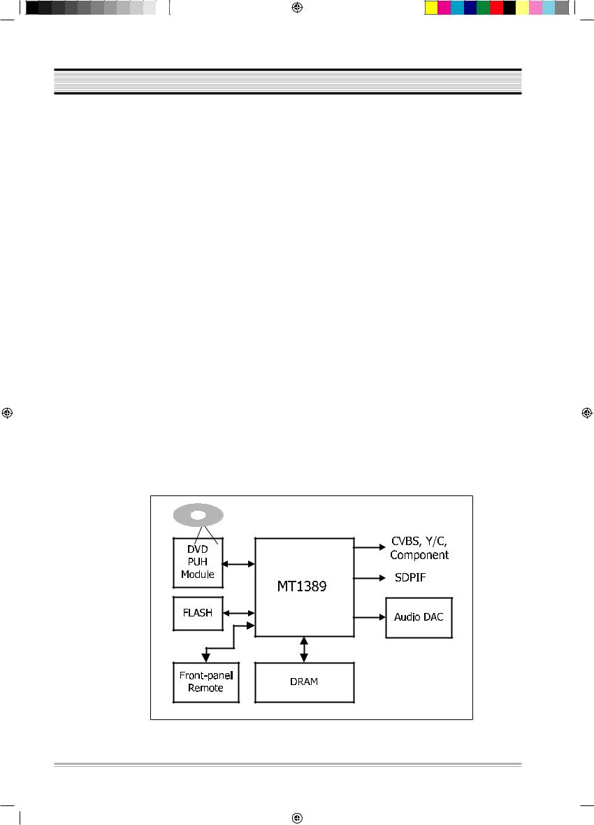
1) DVD Servo And MPEG-2 Decoder : MT1389
MediaTek MT1389 is a DVD player system-on-chip (SOC) which incorporates advanced features like high quality TV encoder and state-of-art de-interlace processing. The MT1389 enables consumer electronics manufacturers to build high quality, cost-effec- tive DVD players, portable DVD players or any other home entertainment audio/video devices.
Based on MediaTek’s world-leading DVD player SOC architecture, the MT1389 is the 3rd generation of the DVD player SOC. It integrates the MediaTek 2nd generation front-end analog RF amplifier and the Servo/MPEG AV decoder.
The progressive scan of the MT1389 utilized advanced motion-adaptive de-interlace algorithm to achieve the best movie/video playback. It also supports a 3:2 pull down algorithm to give the best film effect. The 108MHz/12-bit video DAC provides users a whole new viewing experience.
DVD Player System Diagram
Sm(DAEWOO_1389C)060109.indd |
6 |
|
|
2006-1-13 |
15:41:59 |
|
|
||||
|
|
|
|
|
|
|
|
|
|
|
|
CIRCUIT OPERATIONAL DESCRIPTION
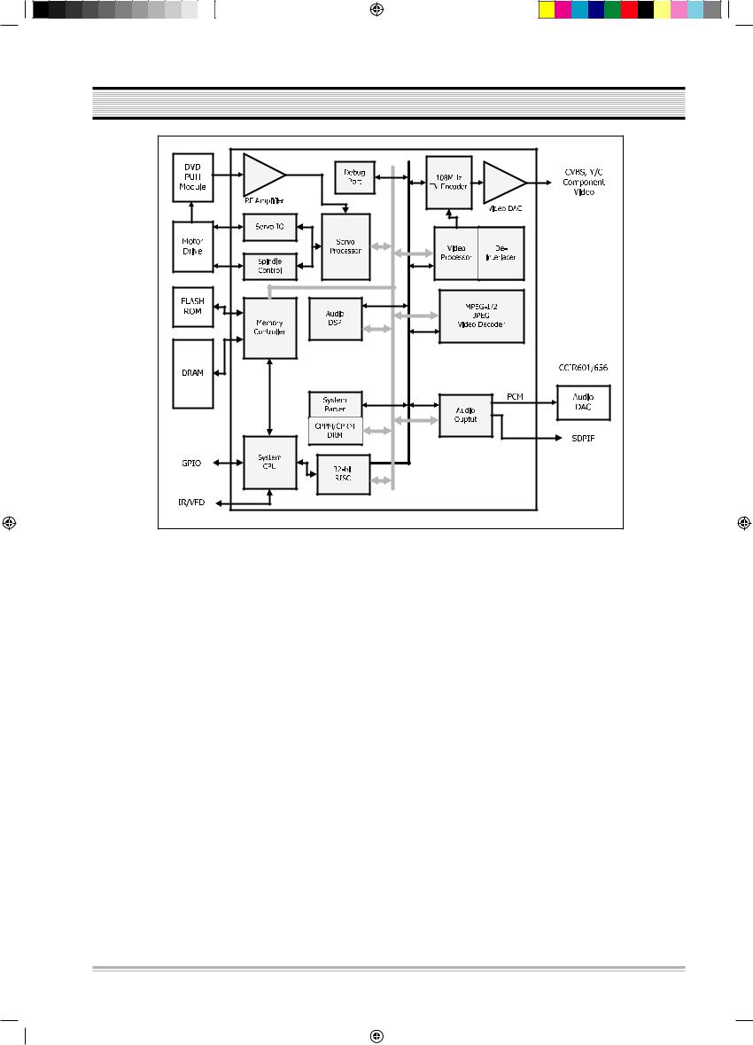
MT1389 Functional Block Diagram
Sm(DAEWOO_1389C)060109.indd |
7 |
|
|
2006-1-13 |
15:42:00 |
|
|
||||
|
|
|
|
|
|
|
|
|
|
|
|

CIRCUIT OPERATIONAL DESCRIPTION
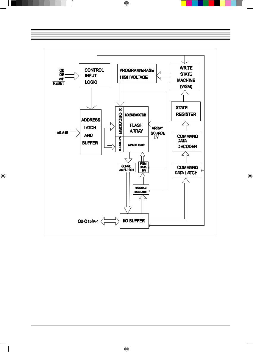
2) Flash Memory : MX26LV800T/B(DV-1000S/DV-1100S/DV-1200S/DV-1300S/DV-1400S/DV-710S)
Description
The MX26LV800T/B is a 8-mega bit high speed Flash memory organized as 1M bytes of 8 bits or 512K words of 16 bits. MXIC's high speed Flash memories offer the most cost-effective and reliable read/write non-volatilerandom access memory. The MX26LV800T/B is pack-aged in 44-pin SOP, 48-pin TSOP, and 48-ball CSP. It is designed to be reprogrammed and erased in system or in standard EPROM programmers.
The standard MX26LV800T/B offers access time as fast as 55ns, allowing operation of high-speed microprocessors without wait states. To eliminate bus contention, the MX26LV800T/B has separate chip enable (CE) and output enable (OE) controls.
MXIC's high speed Flash memories augment EPROM functionality with in-circuit electrical erasure and programming. The MX26LV800T/B uses a command register to manage this functionality. The command register allows for 100% TTL level control inputs and fixed power supply levels during erase and programming, while main-taining maximum EPROM compatibility.
MXIC high speed Flash technology reliably stores memory contents even after 100 erase and program cycles. The MXIC cell is designed to optimize the erase and programming mechanisms. In addition, the combination of advanced tunnel oxide processing and low in-ternal electric fields for erase and program operation sproduces reliable cycling. The MX26LV800T/B uses a3.0V~3.6V VCC supply to perform the High Reliability Erase and auto Program/Erase algorithms.
The highest degree of latch-up protection is achieved with MXIC's proprietary non-epi process. Latch-up protection is proved for stresses up to 100 milliamperes on address and data pin from -1V to VCC + 1V.
Sm(DAEWOO_1389C)060109.indd |
8 |
|
|
2006-1-13 |
15:42:01 |
|
|
||||
|
|
|
|
|
|
|
|
|
|
|
|
CIRCUIT OPERATIONAL DESCRIPTION
FLASH MX26LV800T/B Block Diagram
Sm(DAEWOO_1389C)060109.indd |
9 |
|
|
2006-1-13 |
15:42:01 |
|
|
||||
|
|
|
|
|
|
|
|
|
|
|
|
CIRCUIT OPERATIONAL DESCRIPTION
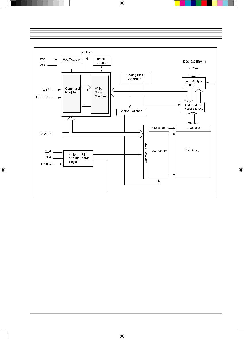
Flash Memory : ES29LV160DB-70TG (DV-760S/DV-1350S/DV-1450S)
Description
The ES29LV160 is a 16 megabit, 3.0 volt-only flashmemory device, organized as 2M x 8 bits (Bytemode) or 1M x 16 bits (Word mode) which is config-urable by BYTE#. Four boot sectors and thirty onemain sectors are provided : 16Kbytes x 1, 8Kbytesx 2, 32Kbytes x 1 and 64Kbytes x 31. The device ismanufactured with ESI’s proprietary, high performance and highly reliable 0.18um CMOS flashtechnology. The device can be programmed orerased in-system with standard 3.0 Volt Vcc supply( 2.7V-3.6V) and can also be programmed in stan-dard EPROM programmers. The device offers min-imum endurance of 100,000 program/erase cyclesand more than 10 years of data retention.
The ES29LV160 offers access time as fast as 70nsor 90ns, allowing operation of highspeed microprocessors without wait states. Three separate controlpins are provided to eliminate bus contention : chipenable (CE#), write enable (WE#) and outputenable (OE#).
All program and erase operation are automaticallyand internally performed and controlled by embed-ded program/erase algorithms built in the device.The device automatically generates and times thenecessary high-voltage pulses to be applied to thecells, performs the verification, and counts the number of sequences. Some status bits (DQ7, DQ6 andDQ5) read by data# polling or toggling betweenconsecutive read cycles provide to the users theinternal status of program/erase operation: whetherit is successfully done or still being progressed.
The ES29LV160 is completely compatible with theJEDEC standard command set of single power sup-ply Flash. Commands are written to the internalcommand register using standard write timings ofmicroprocessor and data can be read out from thecell array in the device with the same way as used inother EPROM or flash devices.
10
Sm(DAEWOO_1389C)060109.indd |
10 |
|
|
2006-1-13 |
15:42:02 |
|
|
||||
|
|
|
|
|
|
|
|
|
|
|
|
CIRCUIT OPERATIONAL DESCRIPTION
FLASH ES29LV160 Block Diagram
11
Sm(DAEWOO_1389C)060109.indd |
11 |
|
|
2006-1-13 |
15:42:03 |
|
|
||||
|
|
|
|
|
|
|
|
|
|
|
|
CIRCUIT OPERATIONAL DESCRIPTION
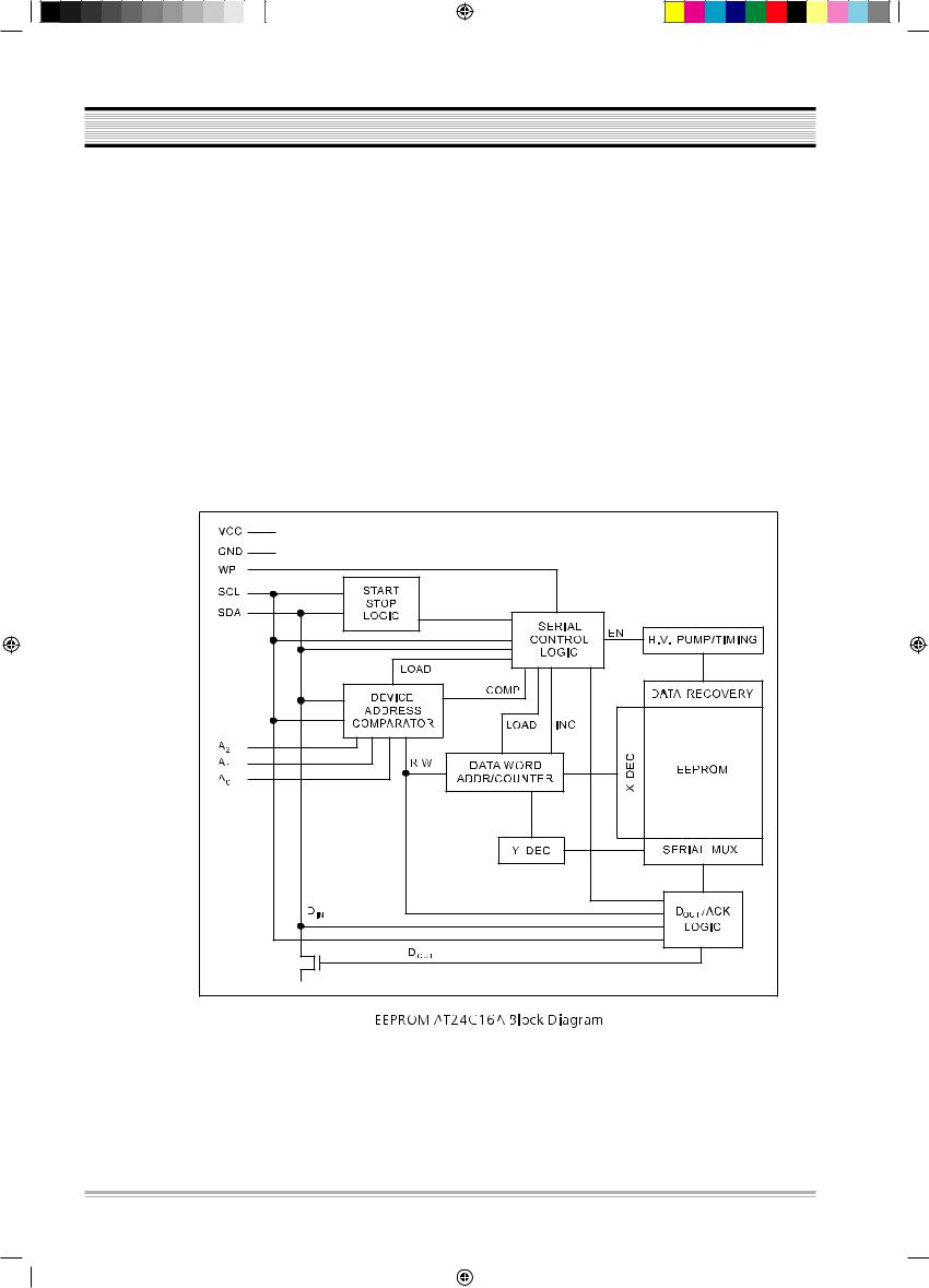
3) EEPROM : AT24C16A
This stores the information related to setup of DVD menus. This can read and write the optional information such as OSD, voice, language option after function for subtitle etc, the aspect or method of TV display, video option like display function and audio, screen saver, parental function through the I2C transmission method.
Description
The AT24C16A provides 16384 bits of serial electrically erasable and programmable read only memory (EEPROM) organized as 2048 words of 8 bits each. The device is optimized for use in many industrial and commercial applications where low power and low voltage operation are essential. The AT24C16A is available in space saving 8-lead PDIP, 8-lead JEDEC SOIC, 8-lead MAP and 8-lead TSSOP packages and is accessed via a 2-wire serial interface. In addition, the entire family is available in 2.7V (2.7V to 5.5V) and 1.8V (1.8V to 5.5V) versions.
12
Sm(DAEWOO_1389C)060109.indd |
12 |
|
|
2006-1-13 |
15:42:03 |
|
|
||||
|
|
|
|
|
|
|
|
|
|
|
|

CIRCUIT OPERATIONAL DESCRIPTION
4) SDRAM : HY57V161610ET-7 (DV-1000S/DV-1100S/DV-1200S/DV-1300S/DV-1400S/DV-710S)
This sends and receives data with MPEG decoder and performs the video signal processing. Every video signal output from DVD player is once stored in SDRAM and then encoded in MPEG decoder and finally output into the analog signal.
SDRAM applied to DVD module has the capacity of 16MBit(1048576 x 16bit x 1Bank), sends and receives data with MPEG decoder by 16 bit.
Description
THE Hynix HY57V161610E is a 16,777,216 bits CMOS Synchronous DRAM, ideally suited for the main memory and graphic appli-cations which require large memory density and high bandwidth. HY57V161610E is organized as 2banks of 524,288x16.
HY57V161610E is offering fully synchronous operation referenced to a positive edge clock. All inputs and outputs are synchronizedwith the rising edge of the clock input. The data paths are internally pipelined to achieve very high bandwidth. All input and outputvoltage levels are compatible with LVTTL.
Programmable options include the length of pipeline (Read latency of 1,2 or 3), the number of consecutive read or write cycles initi-ated by a single control command (Burst length of 1,2,4,8 or full page), and the burst count sequence(sequential or interleave). Aburst of read or write cycles in progress can be terminated by a burst terminate command or can be interrupted and replaced by anew burst read or write command on any cycle. (This pipeline design is not restricted by a `2N` rule.)
13
Sm(DAEWOO_1389C)060109.indd |
13 |
|
|
2006-1-13 |
15:42:03 |
|
|
||||
|
|
|
|
|
|
|
|
|
|
|
|
CIRCUIT OPERATIONAL DESCRIPTION
Refresh
Interval Timer
Address[0:10]
|
CLK |
|
|
|
CKE |
|
|
BA(A11) |
|
||
|
|
Machine |
|
|
|
RAS |
|
|
|
CS |
|
|
|
|
State |
|
|
|
|
|
CAS |
|
|
WE 
UDQM
LDQM
Self Refresh Counter |
Addr.RowLatch/Predecoder |
RowDecoder |
|
|
RefreshAuto/Self |
Addr.[0:11]Ref. |
|
||
|
Refresh |
|
|
|
|
Counter |
|
|
512Kx16 |
|
|
|
|
Bank 0 |
|
|
|
|
Sense AMP & I/O gates |
|
|
|
|
Column Decoder |
|
|
|
|
|
|
|
|
|
|
|
|
|
|
|
|
|
|
|
|
|
|
|
|
DQ0 |
Precharge |
Address |
|
|
|
|
|
|
|
|
|
|
|
|
|
|
|
|
|
|
Buffers |
DQ1 |
|||
|
|
|
|
|
|
|
|
|
|
|
|
|
|
|
|
|
|
|||||||
Row Active |
Register |
|
|
|
|
|
|
|
|
|
|
|
|
|
|
|
|
|
|
DQ2 |
||||
|
|
|
|
|
|
|
|
|
|
|
|
|
|
|
|
|
|
|
|
DQ4 |
||||
|
|
|
|
|
|
|
|
|
|
|
|
|
|
|
|
|
|
|
|
|
|
DQ3 |
||
Column Active |
|
|
|
|
|
|
|
|
|
|
|
Column Addr. |
|
|
|
|
|
|
Input/Output |
DQ5 |
||||
|
|
|
|
|
|
|
|
|
|
|
|
|
|
|
|
|
DQ10 |
|||||||
|
Counter |
|
|
|
|
|
|
|
|
|
|
|
|
|
|
|
|
|
|
|||||
|
|
|
|
|
|
|
|
|
|
|
|
|
Latch & Counter |
|
|
|
|
|
|
|
|
DQ6 |
||
|
|
|
|
|
|
|
|
|
|
|
|
|
|
|
|
|
|
|
|
|
|
|
|
DQ7 |
|
Burst Length |
|
|
|
|
Overflow |
|
|
|
|
|
|
|
|
|
|
|
DQ8 |
||||||
|
|
|
|
|
|
|
|
|
|
|
|
|
|
|
|
|
|
|
|
|
DQ9 |
|||
|
|
|
|
|
|
|
|
|
|
|
|
|
|
|
|
|
|
|
|
|
|
Data |
DQ11 |
|
|
|
|
|
|
|
|
|
|
|
|
|
|
|
|
|
|
|
|
|
|
|
|||
|
|
|
|
|
|
|
|
|
|
|
|
|
|
|
|
|
|
|
|
|
|
DQ12 |
||
|
|
|
|
|
|
|
|
|
|
|
|
|
|
|
|
|
|
|
|
|
|
|
|
DQ13 |
|
|
|
|
|
|
|
|
|
|
|
|
|
|
|
|
|
|
|
|
|
|
|
|
DQ14 |
|
|
|
|
|
|
|
|
|
|
|
|
Column Decoder |
|
|
|
|
|
|
|
|
|
|||
|
|
|
|
|
|
|
|
|
|
|
|
|
|
|
|
|
|
|
|
|
DQ15 |
|||
|
|
|
|
|
|
|
|
|
|
|
Sense AMP & I/O gates |
|
|
|
|
|
|
|
|
|
||||
|
|
|
|
|
|
|
|
|
|
|
|
|
|
|
|
|
|
|
|
|
||||
|
|
|
|
|
|
|
Latch/PredecoderAddr.Row |
|
|
|
|
512Kx16 |
|
|
|
|
|
|
|
|
|
|
||
|
|
|
|
|
|
|
|
|
|
|
|
|
Bank 1 |
|
|
|
|
|
|
|
|
|
|
|
|
|
|
|
|
|
|
|
|
|
|
|
|
|
|
|
|
|
|
|
|
|
|
||
|
|
|
|
|
|
|
|
|
|
|
|
|
|
|
|
|
|
|
|
|
|
|
|
|
Mode Register |
|
|
|
|
|
|
|
|
|
|
Test Mode |
|
|
|
|
I/O Control |
|
|||||||
SDROM HY57V161610E Block Diagram
14
Sm(DAEWOO_1389C)060109.indd |
14 |
|
|
2006-1-13 |
15:42:04 |
|
|
||||
|
|
|
|
|
|
|
|
|
|
|
|

CIRCUIT OPERATIONAL DESCRIPTION
SDRAM : AW39S2016-7 (DV-760S/DV-1350S/DV-1450S)
Description
The AW39S2016-7s organlzed as 2-bank x 1,048,576-word x 16-bit(2Mx16), fabricated with high performance CMOS technology, Synchronous design allows precise cycle control with the use of system clock I/O transactions are possible on every clock cycle. Range of operating frequencies, programmable burst length and programmable latencies allow the same device to be useful for a variety of high bandwidth, high performance memory system applications.
CLK |
|
|
|
|
|
CLOCK |
|
|
|
|
|||||||||
|
|
|
|
|
|
|
|
||||||||||||
|
|
|
|
|
|
|
|
|
|
|
|
|
|
|
|
|
|||
CKE |
|
|
|
|
|
BUFFER |
|
|
|
|
|||||||||
|
|
|
|
|
|
|
|
|
|
|
|
||||||||
|
|
|
|
|
|
|
|
|
|
||||||||||
|
|
|
|
|
|
|
|
|
|
|
|
|
|
|
|
|
|
|
|
|
|
|
|
|
|
|
|
|
|
|
|
|
|
|
|
|
CONTROL |
|
|
|
|
CS |
|
|
|
|
|
|
|
|
|
|
|
|
|
SIGNAL |
|
||
|
|
|
|
|
|
|
|
|
|
||||||||||
|
|
|
|
|
|
|
|
|
|
|
|
|
|
|
|
|
|
|
|
|
|
|
|
|
|
|
|
|
|
|
|
|
|
|
|
|
GENERATOR |
|
|
RAS |
|
|
|
|
|
COMMAND |
|
|
|
|
|||||||||
|
|
|
|
|
|
|
|
||||||||||||
|
|
|
|
|
|
|
|
|
|
|
|
|
|
|
|
||||
CAS |
|
|
|
|
|
DECODER |
|
|
|
|
|||||||||
|
|
|
|
|
|
|
|
||||||||||||
|
|
|
|
|
|
|
|
|
|
|
|
|
|
|
|
|
|||
|
|
|
|
|
|
|
|
|
|
|
|
|
|
|
|||||
|
WE |
|
|
|
|
|
|
|
|
||||||||||
A10 |
|
|
|
|
|
|
|
|
|
|
|
||||||||
|
|
|
|
|
|
|
|
|
|
|
|||||||||
|
|
|
|
|
|
|
|
|
|||||||||||
|
A0 |
|
|
|
|
|
|
|
|
|
|
|
|||||||
|
|
|
|
|
|
|
|
|
|
|
|
||||||||
|
|
|
|
ADDRESS |
|
|
|
|
|||||||||||
|
|
|
|
|
|
||||||||||||||
|
|
|
|
|
|
|
|
|
|
|
|||||||||
|
|
|
|
|
|
|
|
|
|
|
|
||||||||
|
|
A9 |
|
|
|
|
|||||||||||||
|
|
|
|
||||||||||||||||
A11 |
BUFFER |
|
|
|
|
||||||||||||||
BS0 |
|
|
|
|
|
|
|
||||||||||||
BS1 |
|
|
|
|
|
|
|
||||||||||||
|
|
|
|
|
|
|
|
|
|
|
|
|
|
|
|
|
|
|
|
REFRESH
COUNTER
ROW DECODER
ROW DECODER |
ROW DECODER
ROW DECODER
COLUMN DECODER
CELL ARRAY
BANK #1
SENSE AMPLIFIER
DQ
BUFFER
DQ0
DQ15
UDQM
LDQM
COLUMN DECODER
CELL ARRAY
BANK #3
SENSE AMPLIFIER
NOTE:
The cell array configuration is 4096 * 256 * 16
SDROM AW39S2016-7 Block Diagram
15
Sm(DAEWOO_1389C)060109.indd |
15 |
|
|
2006-1-13 |
15:42:04 |
|
|
||||
|
|
|
|
|
|
|
|
|
|
|
|
CIRCUIT OPERATIONAL DESCRIPTION
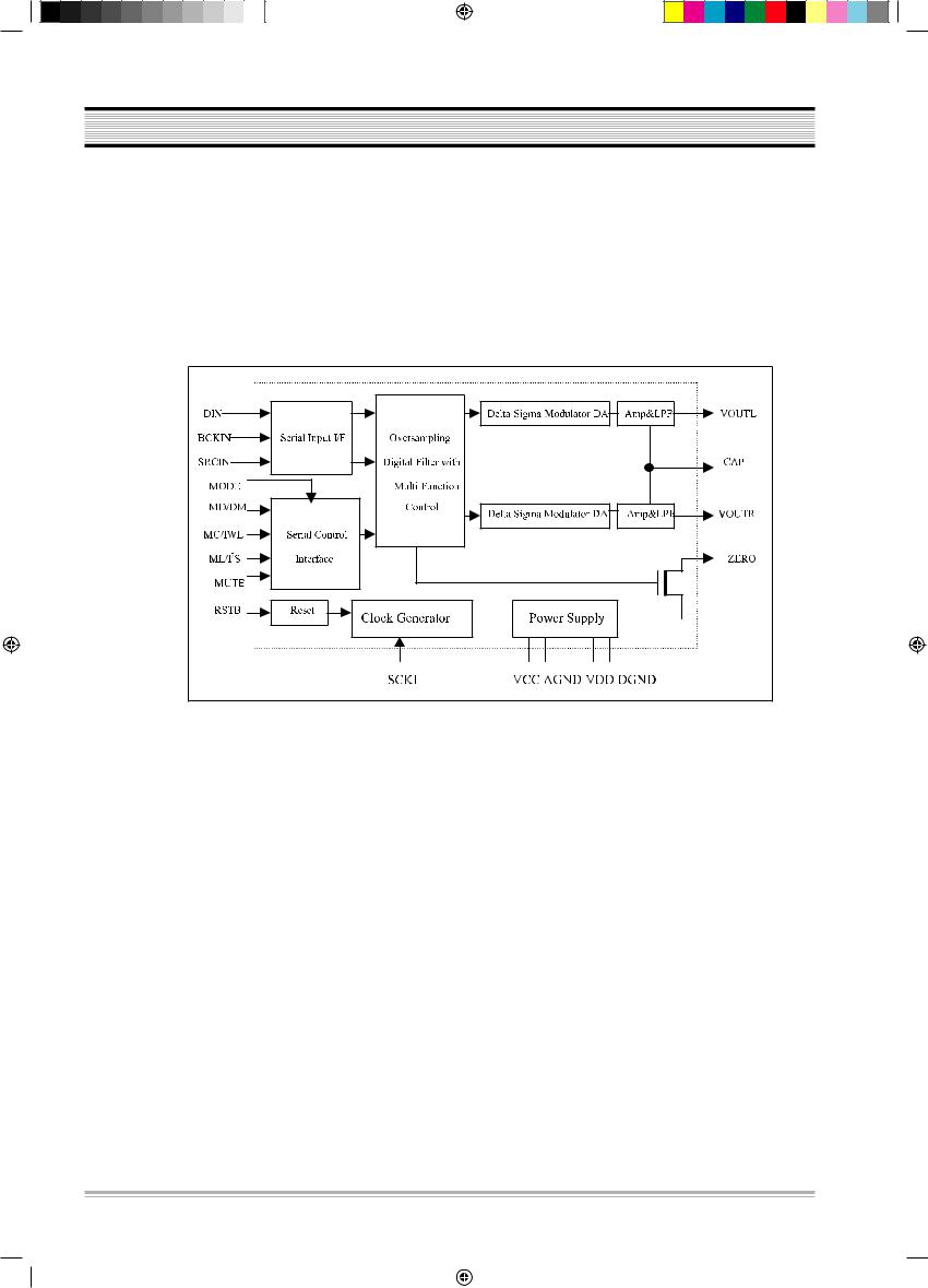
5) DAC : DA1132 (DV-1000S/DV-1100S/DV-1200S/DV-1300S/DV-1400S/DV-710S)
Description
DA1132 is a high performance stereo digital to analog converter for consumer electronics applications such as, VCD/DVD player, DVD-ROM driver, MPEG2 card, set-top box, and home theaters etc. It accepts input word length of 16, 18, 20, and 24bits and supports audio sampling frequency from 16KHz to 96KHz. In addition DA1132 provides a range of control features either via 3-wire serial interface ports or hardware pins.
DAC DA1132 Block Diagram
16
Sm(DAEWOO_1389C)060109.indd |
16 |
|
|
2006-1-13 |
15:42:05 |
|
|
||||
|
|
|
|
|
|
|
|
|
|
|
|
CIRCUIT OPERATIONAL DESCRIPTION
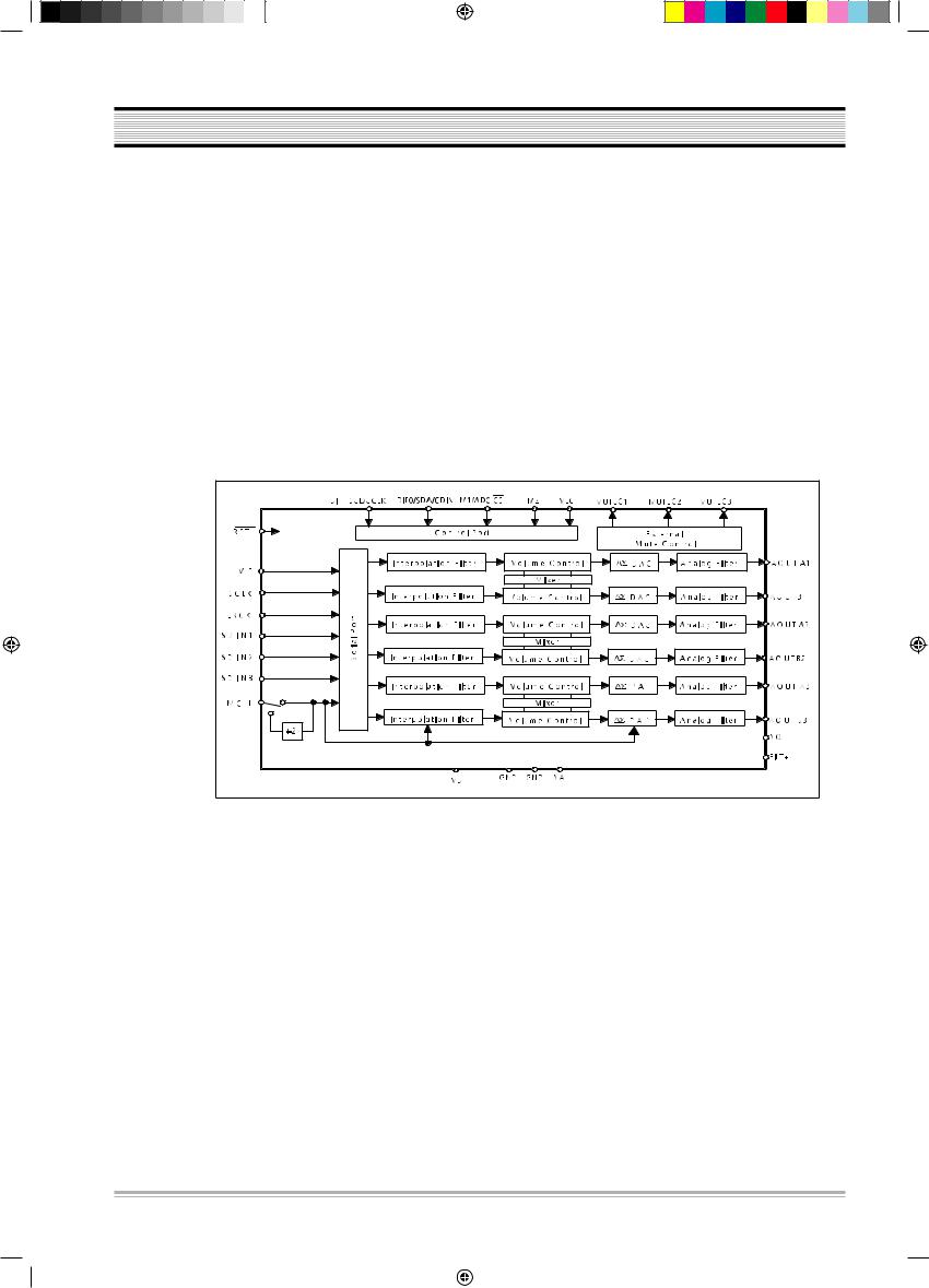
DAC : CS4360 (DV-760S/DV-1350S/DV-1450S)
Description
The CS4360 is a complete 6-channel digital-to-analog system including digital interpolation, fourth-order delta-sigma digital-to-analog conversion, digital deemphasis, volume control, channel mixing and analog filtering. The advantages of this architecture include: ideal differential linearity, no distortion mechanisms due to resistor matching errors, no linearity drift over time and tempera-ture and a high tolerance to clock jitter.
The CS4360 accepts data at audio sample rates from 4kHz to 200kHz, consumes very little power and operates over a wide power supply range. These features are ideal for cost-sensitive, multi-channel audio systems including DVD players, A/V receivers, set-top boxes, digital TVs and VCRs, mini-component systems, and mixing consoles.
DAC CS4360 Block Diagram
17
Sm(DAEWOO_1389C)060109.indd |
17 |
|
|
2006-1-13 |
15:42:06 |
|
|
||||
|
|
|
|
|
|
|
|
|
|
|
|

VOLTAGE CHARTS
Power board output voltage
J1
|
Pin number |
1 |
2 |
3 |
4 |
5 |
6 |
7 |
8 |
9 |
|
|
|
|
|
|
|
|
|
|
|
|
Output voltage |
GND |
S5V |
3.3V |
D5V |
GND |
A5V |
GND |
+12V |
-12V |
|
|
|
|
|
|
|
|
|
|
|
|
J2 |
|
|
|
|
|
|
|
|
|
|
|
|
|
|
|
|
|
|
|
|
|
Pin number |
1 |
2 |
3 |
4 |
5 |
6 |
|
|
|
|
|
|
|
|
|
|
|
|
|
|
|
Output voltage |
SW |
F- |
F+ |
GND |
-24V |
STB5V |
|
|
|
|
|
|
|
|
|
|
|
|
|
|
Decode board input voltage |
|
|
|
|
|
|
|
|
||
|
CN1 |
|
|
|
|
|
|
|
|
|
|
|
|
|
|
|
|
|
|
|
|
|
Pin number |
1 |
2 |
3 |
4 |
5 |
6 |
7 |
8 |
9 |
|
|
|
|
|
|
|
|
|
|
|
|
Output voltage |
GND |
S5V |
3.3V |
D5V |
GND |
A5V |
GND |
+12V |
-12V |
|
|
|
|
|
|
|
|
|
|
|
18
Sm(DAEWOO_1389C)060109.indd |
18 |
|
|
2006-1-13 |
15:42:07 |
|
|
||||
|
|
|
|
|
|
|
|
|
|
|
|
CIRCUIT DIAGRAM
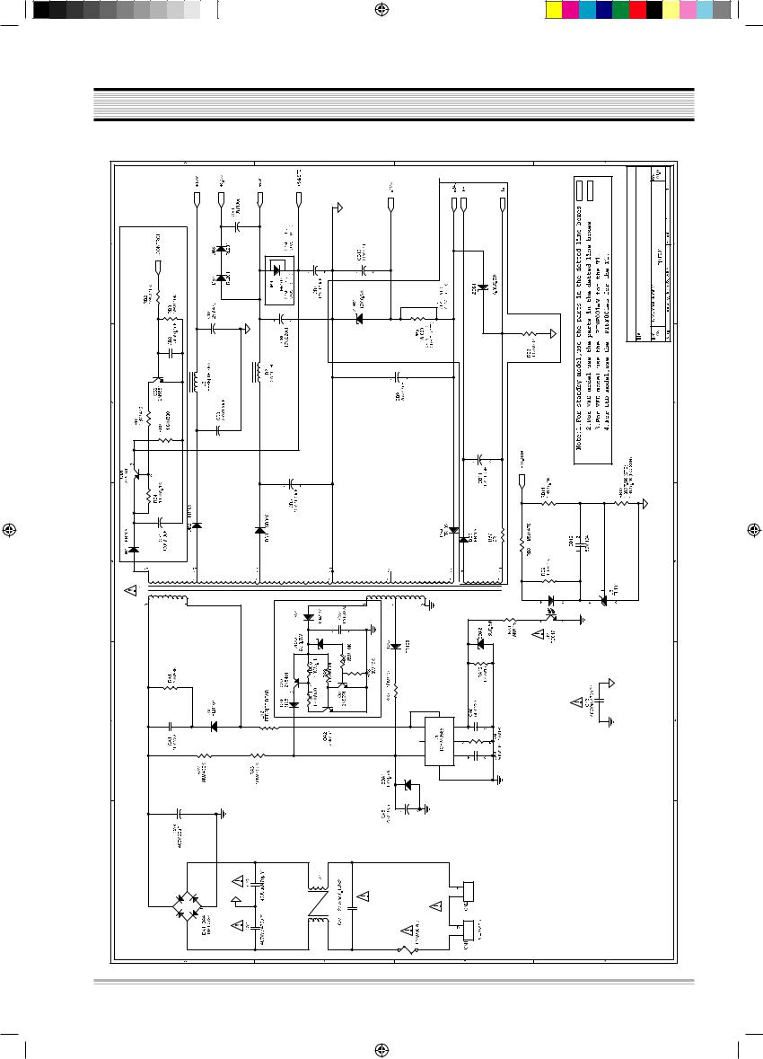
1. POWER SUPPLY SCHEMATIC DIAGRAM
|
|
19 |
|
Sm(DAEWOO_1389C)060109.indd |
19 |
2006-1-13 |
15:42:09 |
CIRCUIT DIAGRAM
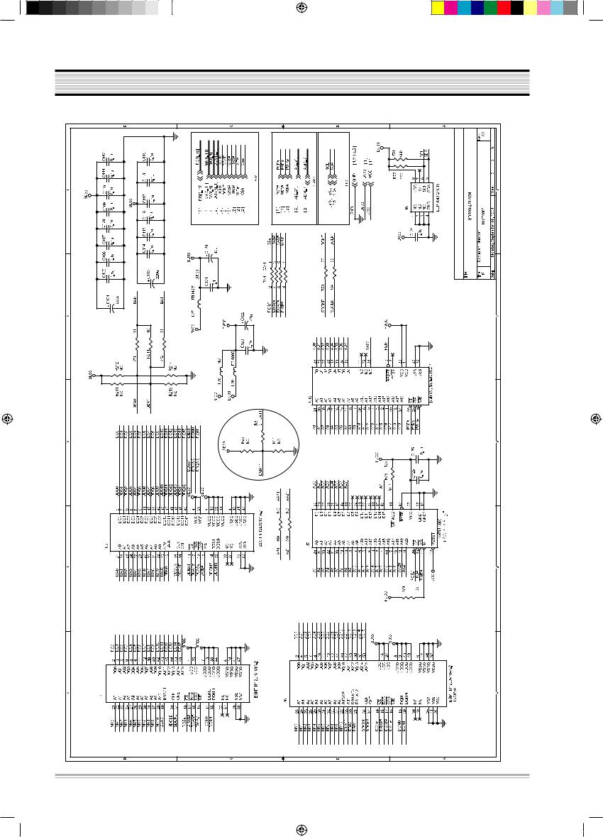
2. DECODE BOARD SCHEMATIC DIAGRAM
1) INDEX SCHEMATIC DIAGRAM
20
Sm(DAEWOO_1389C)060109.indd |
20 |
|
|
2006-1-13 |
15:42:11 |
|
|
||||
|
|
|
|
|
|
|
|
|
|
|
|

CIRCUIT DIAGRAM
2) RF & MPEG SCHEMATIC DIAGRAM
|
|
21 |
|
Sm(DAEWOO_1389C)060109.indd |
21 |
2006-1-13 |
15:42:17 |
CIRCUIT DIAGRAM |
|
|
3) SDRAM & FLASH SCHEMATIC DIAGRAM |
|
|
|
22 |
|
Sm(DAEWOO_1389C)060109.indd 22 |
2006-1-13 |
15:42:21 |
CIRCUIT DIAGRAM
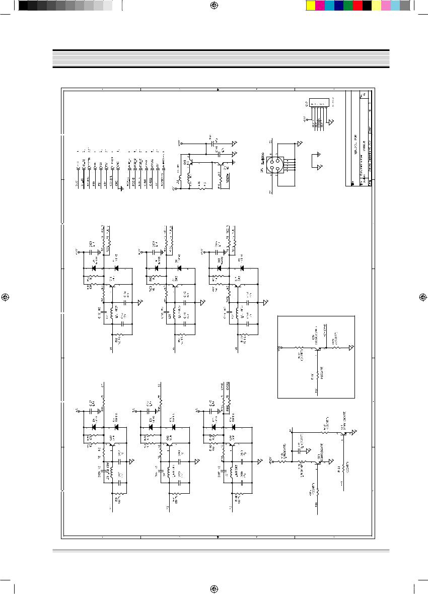
4) VIDEO OUTPUT PORT SCHEMATIC DIAGRAM
|
|
23 |
|
Sm(DAEWOO_1389C)060109.indd |
23 |
2006-1-13 |
15:42:25 |
CIRCUIT DIAGRAM
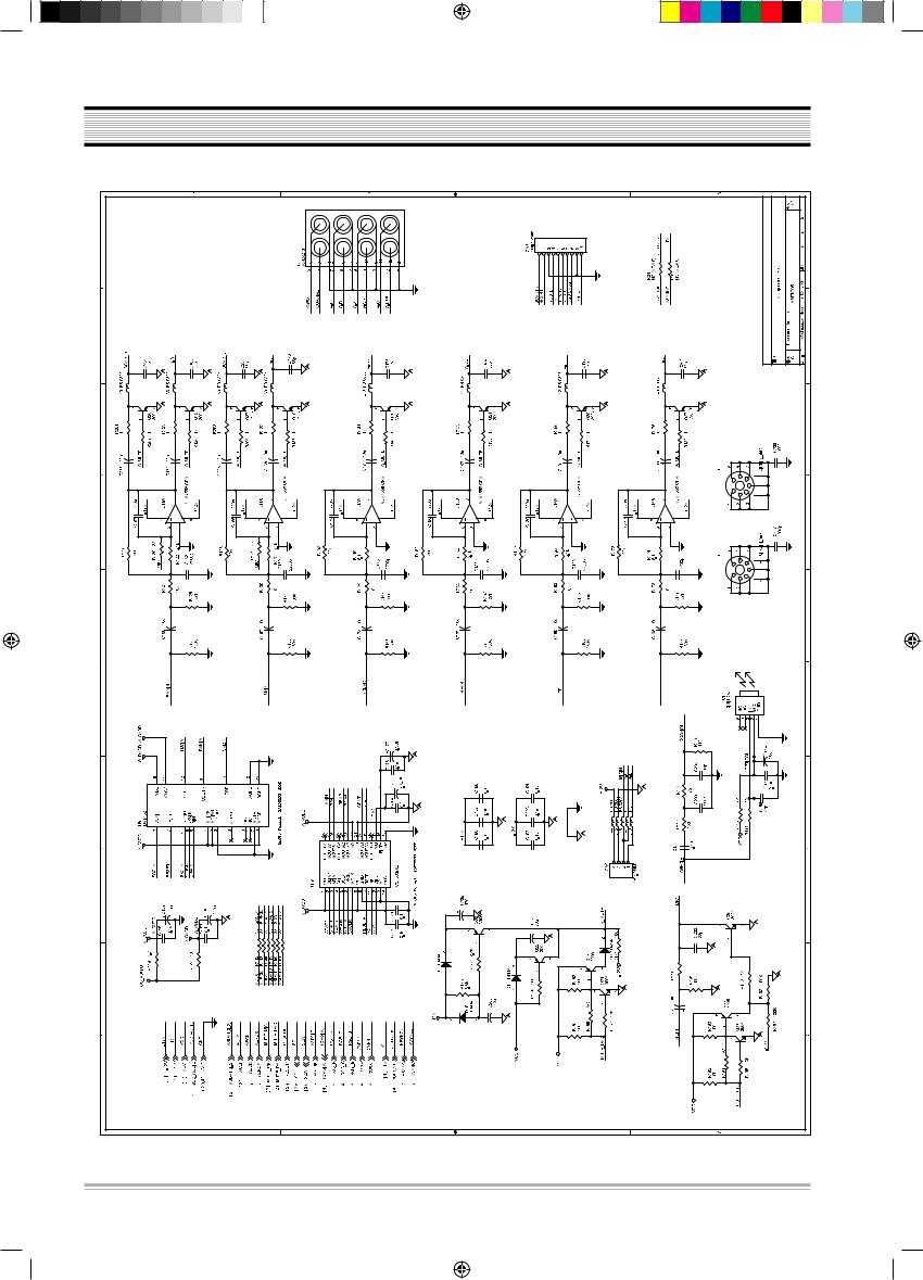
5) AUDIO OUTPUT PORT SCHEMATIC DIAGRAM
|
|
24 |
|
Sm(DAEWOO_1389C)060109.indd |
24 |
2006-1-13 |
15:42:29 |
CIRCUIT DIAGRAM
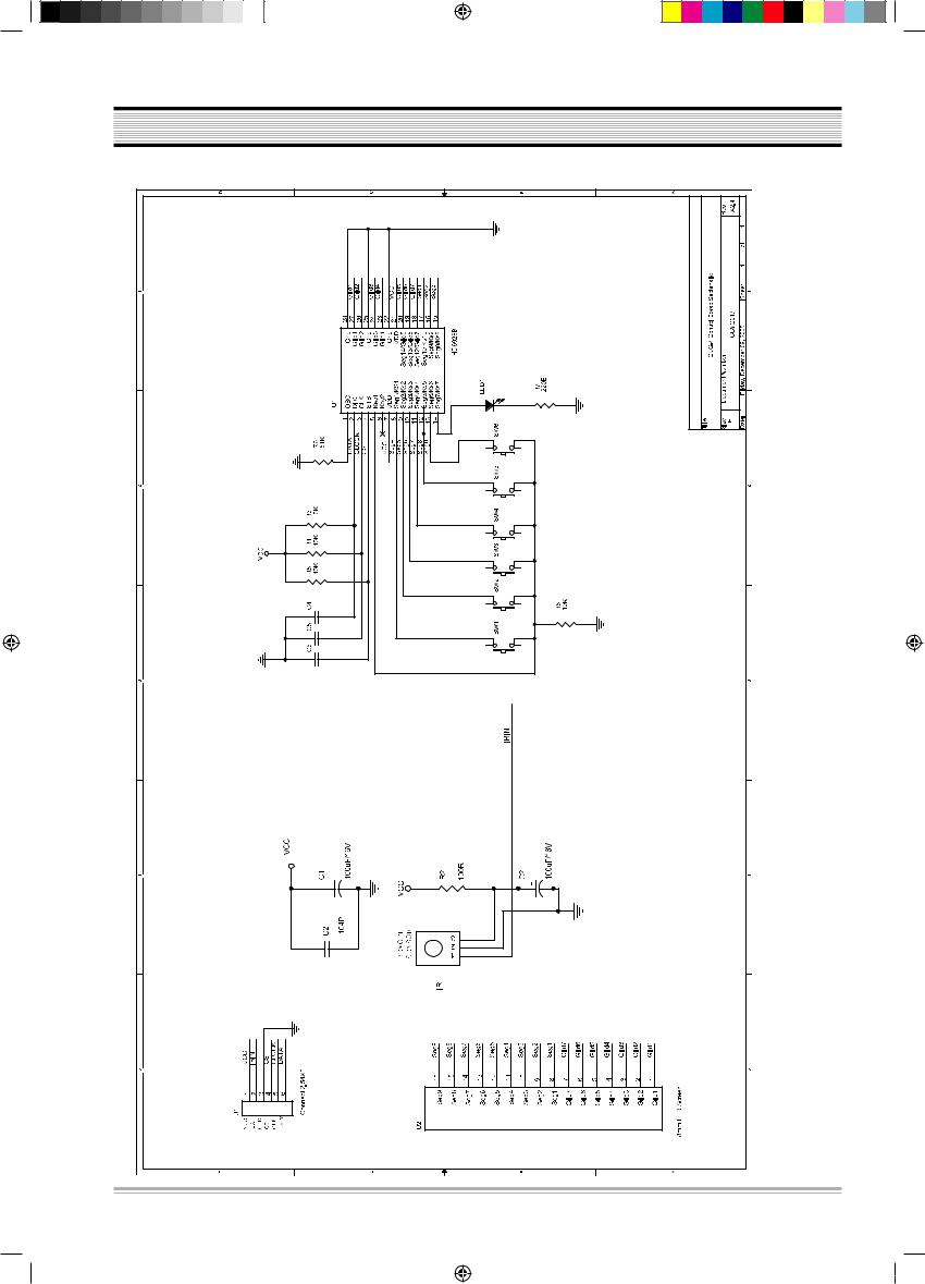
3. CONTROL BOARD SCHEMATIC DIAGRAM (DV-1000S/DV-1100S/DV-710S/DV-760S) |
|
|
|
25 |
|
Sm(DAEWOO_1389C)060109.indd 25 |
2006-1-13 |
15:42:31 |
 Loading...