


DR-M06

DR-M03SX
Service Manual
DR-M06TH
CONTENTS
SPECIFICATIONS PARTS LAST
1) General 2 CPU Unit 22
2) Transmitter 2 MAIN Unit 22~24
3) Receiver 2 VCO Unit 24
CIRCUIT DESCRIPTION SP Unit 25
1) Receiver System 3 Mechanical Parts 25
2) Transmitter System 4 Packing.. 25
3) PLL Circuit 4 DRM03 PA Unit 25
4) Terminal Function of Microprocessor 5 ~ 7
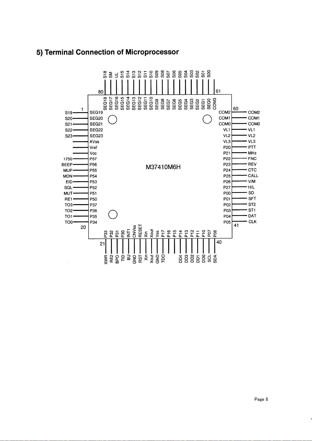
5) Terminal Connection of Microprocessor 8 ADJUSTMENT
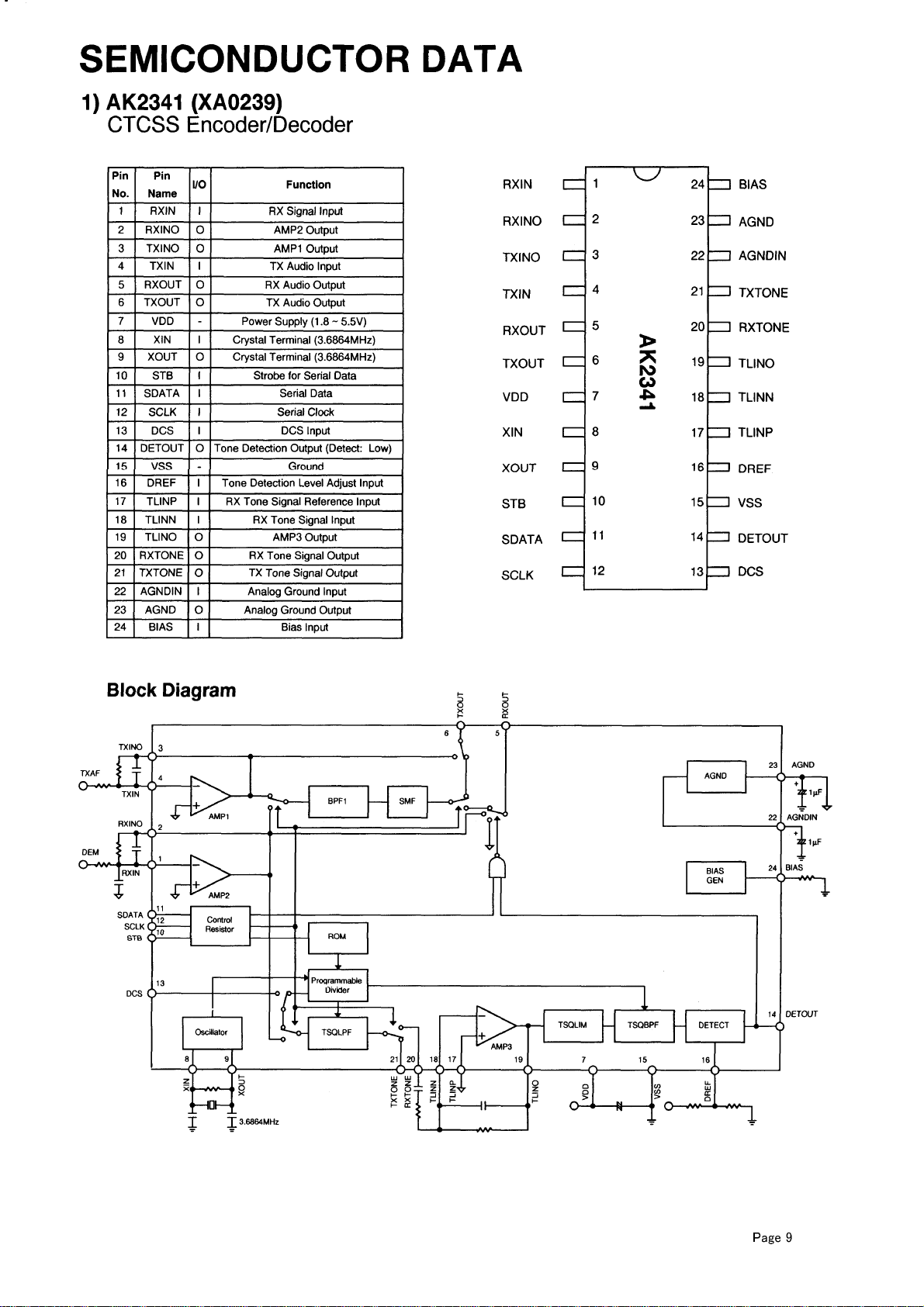
SEMICONDUCTOR DATA 1) Required Test Equipment. 27
1) AK2341 9 2) Adjustment for DR-M06/03 28~29
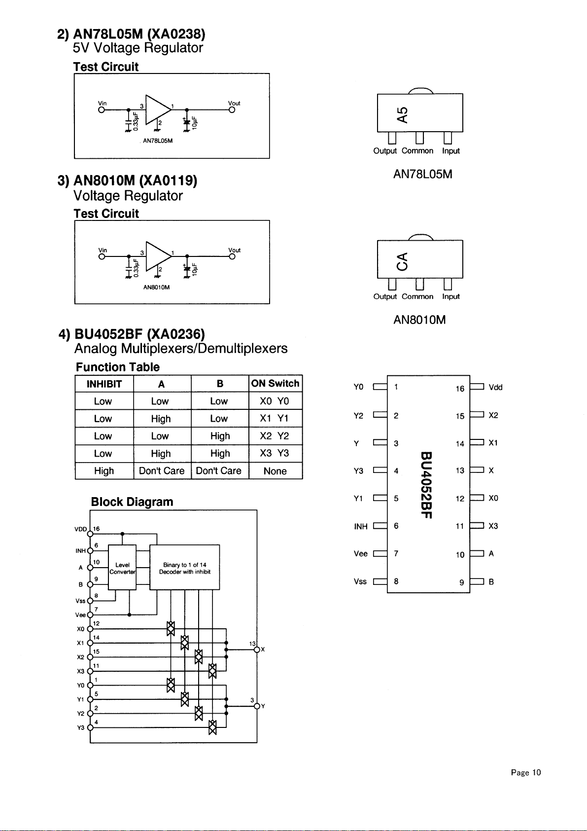
2) AN78L05M 10 3) Adjustment Points 30
3) AN8010M 10 4) Adjustment Quick Reference 30
4) BU4052BF 10
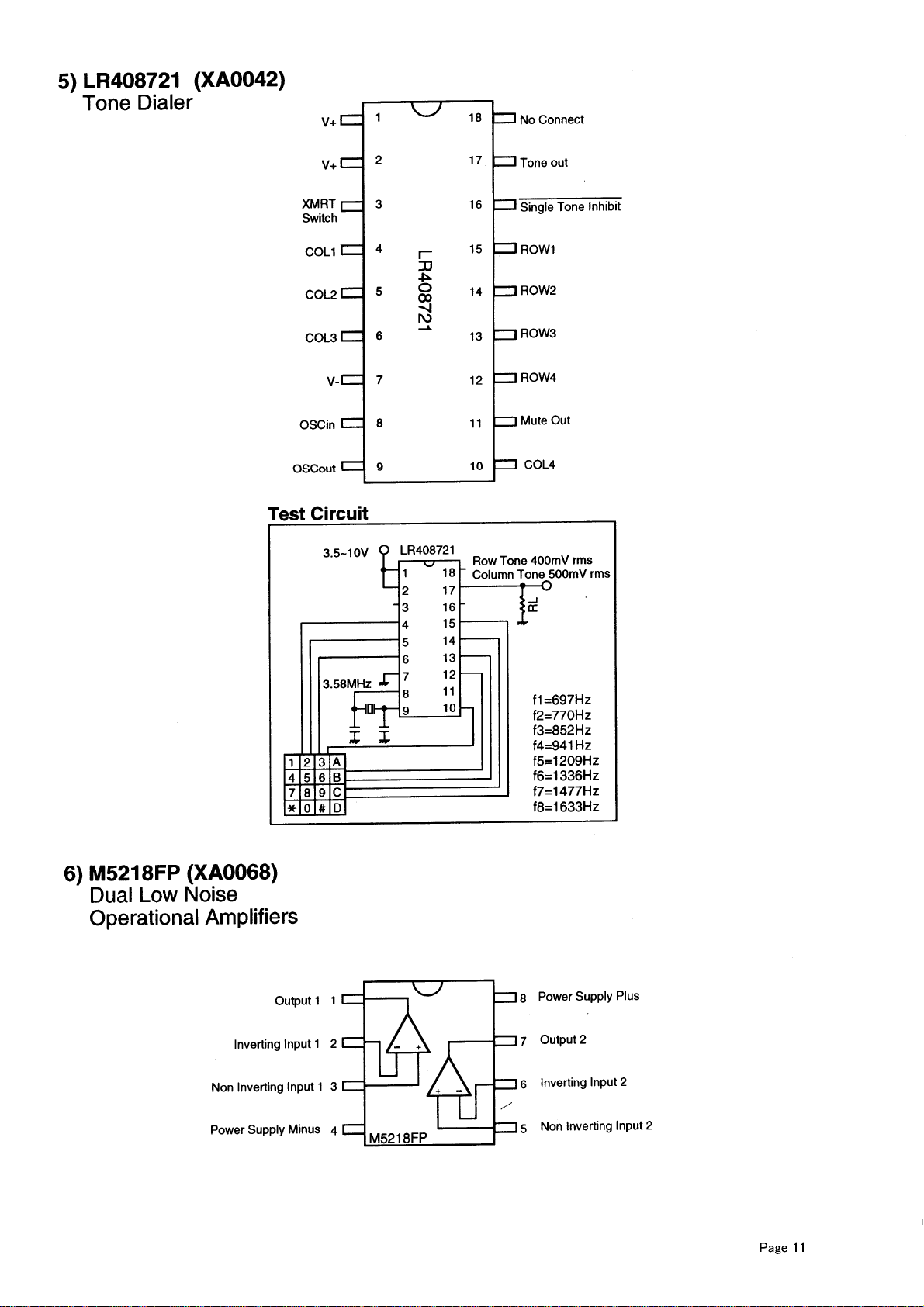
5) LR408721 11 CIRCUIT DIAGRAM
6) M5218FP 11 3) Main Unit 32
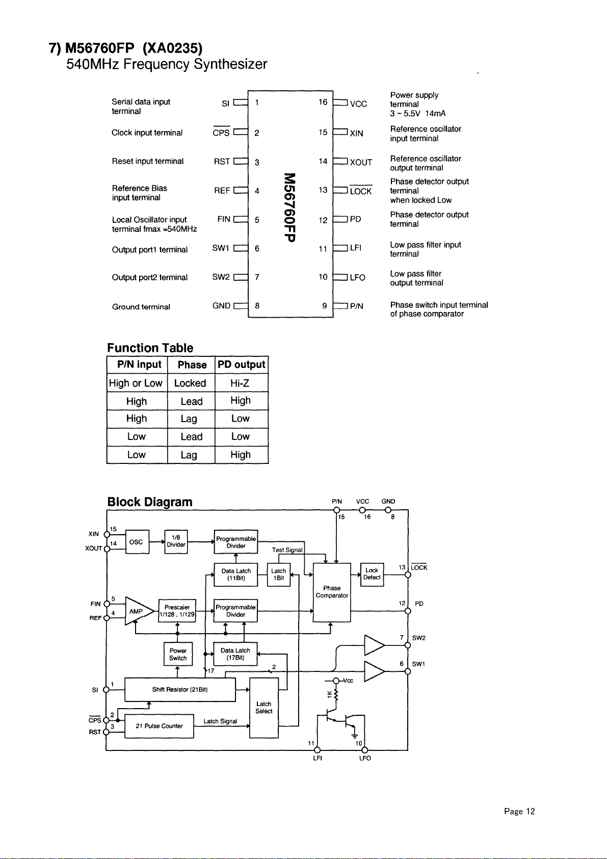
7) M56760FP 12 4) Main Unit 33
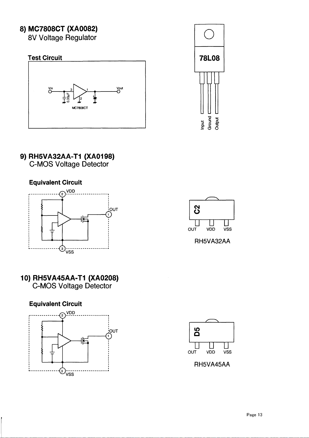
8) MC7808CT 13 5) CPU Unit 34
9) RH5VA32AA-T1 13
10) RH5VA45AA-T1 13 PC BOARD VIEW
11)M57735 14 1) Main Unit Side A 35
12) TK10487MTR 15 2) Main Unit Side B 36
13) AT24C02N-10SI-2.7 15 3) CPU Unit Side A. 37
14) AT24C08-10SI-2.7 15 4) CPU Unit Side B 37
15) uPC1241H 16 5) VCO Unit Side A 38
16) Transistor, Diode and LED Outline Drawings 16 6) VCO Unit Side B 38
17) LCD Connection 17
EXPLODED VIEW
1) Bottom View 18
2) LCD View 18
3) Top, Front View 1 19
4) Top, Front View 2 20
5)DRM03 PA UNIT 21
VERSION TABLE 21
ALINCO INCORPORATED
TWIN 21 M.I.D. TOWER BUILDING 23F, 1-61, 2-CHOME,
SHIROMI CHUO-KU , OSAKA, 540-8580 JAPAN
Tel (81)6-6946-8150 fax (81)6-6946-8175
e-mail: export@alinco.co.jp

* SPECIFICATIONS
A
GENERAL
Frequency DRM03SX 28.00 - 29.700MHz
DRM06TH 50.00 - 54.00MHz
Step 5 , 10 , 12.5 , 15 , 20 , 25 KHz selectable
Channel 100
Modulation F3E (FM)
Antenna impedance 50 ohm unbalanced
Power supply 13.8V DC +/- 10%
Current Tx high.approxl 3.0
Rx squelched.less than 600mA
Dimensions DRM03SX 140(W) x 40(H) x 115(D)
DRM06TH 140(W) x 40(H) x 155(D)
Weight DRM03SX approx 681gs
DRM06TH approx 800gs
Transmitter
Power output DRM03SX High : 10W Low: 1W
DRM06TH High : 20W Low: 2W
Modulation variable reactance frequency modulation
Max deviation +/- 5.0kHz
Spurious -60dB or under below carrier
Microphone Electret Condenser Microphone
Operatin Mode Simplex/Semi-Duplex
Offset 0 to +/-15.995MHz freely programmable
(DRM03SX)
Receiver
Receiver sys Double-conversion superheterodyne
I.F. 10.7MHz and 455kHz
Sensitivity DRM03SX 0.16uV (-16dBu) 12dB SINAD
DRM06DX 0.25uV (-12dBu) 12dB SINAD
Selectivity +/- 6kHz or under at -6dB
+/- 15kHz or under at -60dB
AF Output 2.5W with 8ohm at 10%distortion
8ohm
Page 2

CIRCUIT DESCRTPTION
1) Receiver System
1. Front End The signal from the antenna is passed through a low-pass filter and input to
the voltage step up circuit consisting Of L14. The signal from L14 is led to
the gate of Q1. D19 is the diode limiter circuit against the excessive input
power of more than 20dBm. Q1 is the FETwhich has two gates. The
voltage of the gate 2 is set higher to get the high gain and sensitivity. The
signal from Q1 is led to the triple band pass filter (L4, L5, L6), and gets the
high image rejection ratio.
2. Mixer Circuit The signal from the triple band pass filter is converted into the first IF signal
of 17.2MHz. The receiving signal is led to the gate 1 of Q2, and the first
local oscillator signal is led to the gate 2 of Q2. To get the high conversion
gain, the local oscillator signal voltage is set to about 1V. To reduce the
high adjacent channel interference, the band width of the FL2 is set to
20kHz. The signal from FL2 is amplified by Q8, and input to FM IF system
IC3 of TK10487.
3. IF Circuit The TK10487 has the second local oscilltor circuit, mixer circuit, detector
circuit, squelch circuit, and so on. Pin1 and 2 are the terminals of the crystal
oscillator circuit. Pin2 (emitter) is connected to the ground via the resister
R3 to prevent the oscillator from decreasing the power at the low temperature. Pin4 of IC3 is connected to FL1 directly because the matching resistor
for ceramic filter is built-in. The quadrature circuit (pin10 of IC3) is connected to the ceramic resonator X2 for the temperature stability and good
quality. The signal from pin11 of IC3 is connected to the LPF. The detected
AF signal, which has flat frequency characteristics, is led to the control unit
and used as both squelch signal and tone squelch signal. De-emphasis
circuit consists of R31, R32, C26 and C27. The LPF amplifier consisting of
Q5 and Q6 is located far away from the VR in the control unit, so it outputs
the high voltage signal to prevent S/N from the deterioration. The squelch
switch circuit consists of Q4 and Q16, and switches on/off at the point where
there is no voltage to prevent from the switching noise. The S meter signal
from pin12 of IC3 is led to the CPU in the control unit after adjusting the level
at D20 and VR5. The S meter signal is thermal compensated by TH1 and
stabilized. The noise amplifier consists of pin13 and 14, the built-in OP
amplifier in IC3. The output signal of noise amplifier is amplified by Q14,
rectified by D5, and then led to the pin15 (hysteresis comparator input) of
IC3.
4. AF Circuit IC4 is about 5W audio power amplifier IC. When the capacity of pin1 in C16
is increased more, the output incidental noise becomes smaller. The highpitched tone becomes smaller at the same time, This radio's capacity of
C16 is determined considering the high-pitched tone.
PAGE-3

2) Transmitter System
1. Modulation Circuit
The microphone amplifier IC1 (IDC, LPF) consists of two operational amplifiers. The signal from the microphone is led to pre-emphasis circuit consisting
of C36 and R47 and then to the limiter circuit. The limiter circuit uses the
saturation of the OP amplifier. The amplified signal is input to the low-pass
filter IC1A. The output signal from the microphone amplifier is passed
through variable resistors VR2 for modulatlon adjustment and input to the
VCO unit. Sub tone deviation is determined by R24, R25 and VR2. The
radio does not have the adjustment variable resistor for sub tone deviation.
2. TX Amp. Circuit
The signal from VCO is ampriied by TX, RX wide band LO amplifier Q19.
The signal from Q19 is passed through the transmission/reception selector,
and amplified byQ20 and Q15. The PA unit is driven at 200mW driving
power.
3. PA Circuit
IC5 is 20W(M06DX) powered amplifier module. The output power is controlled by
the voltage of V1. The RF signal amplified 20W in PA is passed through D3
and three-stage transmission/reception low-pass filter, and input to the
antenna connector.
4. ALC Circuit (M06DX)
The power detection circuit consisting of D17 and D18 rectifies the output
signal voltage. The detected DC voltage is led to the VR1 (power adjust
trimmer), and amplified by Q3, Q9 and Q13. Output power is controlled by
voltage of V1 in IC5 and collector voltage of Q15. When the temperature
goes up unusually, the power down circuit consisting of R101 and TH2
works to prevent the device from the destruction.
3)PLL Circuit
(M06DX)
The VCO unit is designed for the PLL circuit, putting the VCO on one side,
and PLL circuit on the other side.
Q301 in the VCO is grounded using the gate oscmator, and its frequency
covers 50MHz to 54MHz without transmission/reception shift circuit.
IC301 is pulse swallow system based PLL IC with the built-in prescaler,
which synthesizes 150MHz-band signal.
The loop filter consisting of Q302 and Q303 is the active type.
PAGE-4
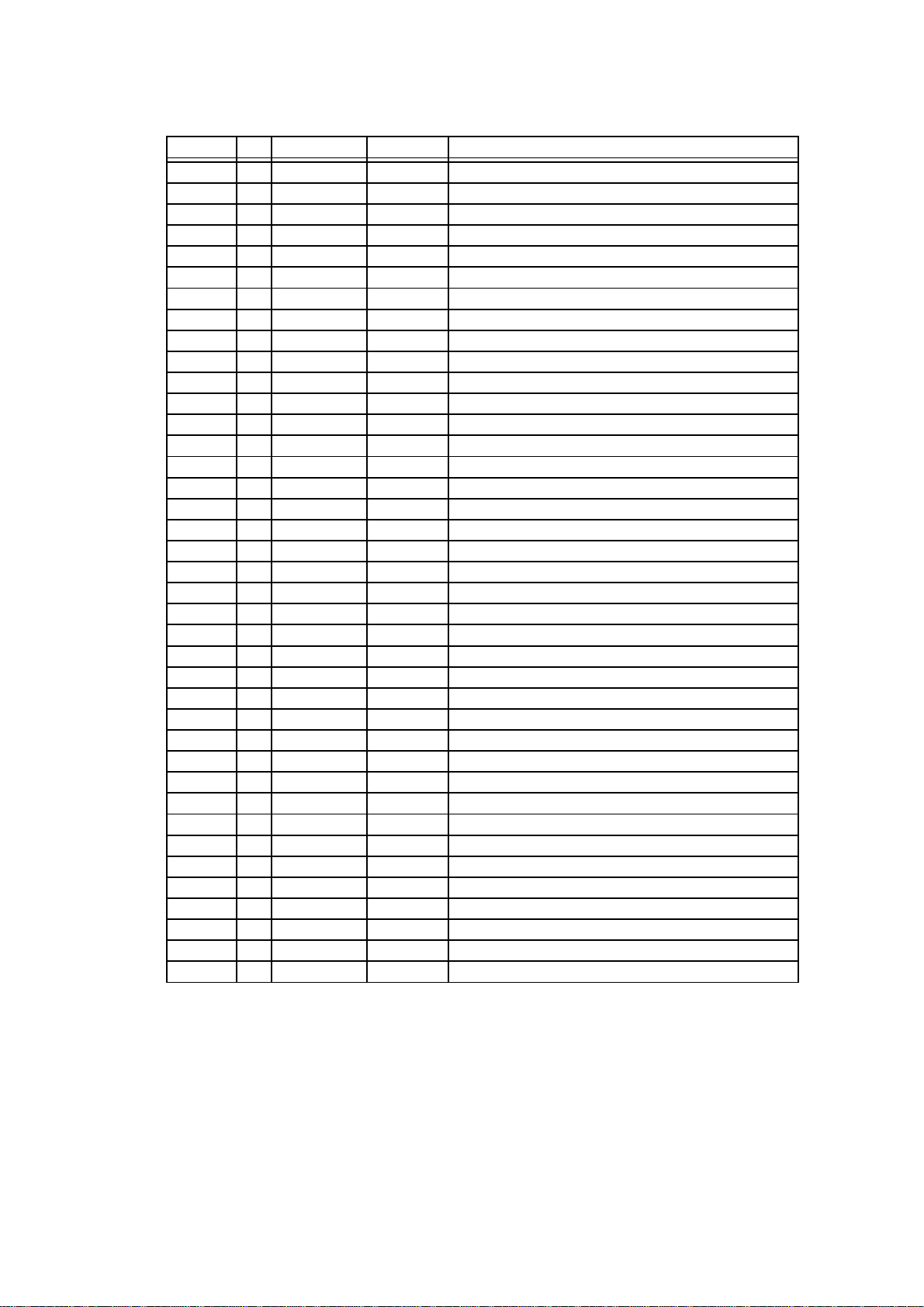
4) Terminal Function of Microprocessor
Port No. I/O Logic PinName Description
1 O SEG19 LCDSegment19 Output
2 O SEG20 LCDSegment20 Output
3 O SEG21 LCDSegment21 Output
4 O SEG22 LCDSegment22 Output
5 O SEG23 LCDSegment23 Output
6 I GND AnalogGround 0V
7 I Vref Reference Voltage Input 5V
8 I Vcc CPU Power Supply hnput 5V
9 O 1750_ ToneBurstOutput
10 O Clock BEEP BeepToneOutput
11 I Active Low MUP Channel Up Input (Microphone Control)
12 I Active Low MDN Channel Down Input (Microphone Control)
13 I NoUse EID
14 O Active Low SQL Squelch Control (L: Audio is off.)
15 O ActiveHigh MUT Microphone Mute (H: Mic Amp is off.)
16 I Active Low REl RotaryEncoder Input
17 O Clock TO3 ToneOutput
18 O Clock TO2 ToneOutput
19 O Clock TO1 ToneOutput
20 O Clock TO0 ToneOutput
21 I ActiveHigh XWR EEPROM Write Status External Input
22 I Active Low RE2 RotaryEncoder Input
23 O Active Low BPO Band Plan Detection Input (Common)
24 I Active Low TID Tone Unit Detection Input
25 I Active Low BU Back Up Signal Detection input
26 I GND Ground
27 l Active Low RST ResetInput
28 I Xin Crystal Oscillator Terminal (3.58MHz)
29 O Xout Crystal Oscillator Terminal (3.58MHz)
30 I GND Ground
31 I Active Low TDO CTCSS Tone Detection Output
32 O Active High DTD For Trunking
33 O NoUse
34 I Active Low DD4 Band Plan 4 (V/U Selection)
35 I Active Low DD3 Band Plan 3 (445/435 Selection)
36 I Active Low DD2 Band Plan 2 (5k/12.5k Selection)
37 I Active Low DD1 Band Plan 1
38 I Active Low DD0 Band Plan 0
39 O Clock SCL Clock Output for EEPROM
PAGE-5
Port No. I/O Logic PinName Description
40 I/O Clock SDA Data Output for EEPROM
41 O Clock CLK Clock Output
42 O Clock DAT DataOutput
43 O Clock ST1 Strobe Output for PLL IC
44 O Clock ST2 Strobe Output for CTCSS IC
45 I Active Low SFT Shift Key Input
46 I Active High SD Signal Detection Input
47 O Active High H/L Transmission Power (H: Low Power)
48 I Active Low V/M VFO/Memory Key Input
49 I Active Low CAL Call Key Input
50 I Active Low CTC CTCSS Mode Set Input
51 I Active Low REV Reverse Key Input
52 I Active Low FNC Function Key Input
53 I Active Low MHz MHzKeyInput
54 I Active Low PTT PTTKeyInput
55 I LV3 Power Supply Input for LCD
56 I LV2 Power Supply Input for LCD
57 I LV1 Power Supply Input for LCD
58 I COM0 LCD Common 0 Output
59 I COM1 LCD Common 1 Output
60 I COM2 LCD Common 2 Output
61 I No Use
62 O SEG00 LCD Segment 00 Output
63 O SEG01 LCD Segment 01 Output
64 O SEG02 LCD Segment 02 Output
65 O SEG03 LCD Segment 03 Output
66 O SEG04 LCD Segment 04 Output
67 O SEG05 LCD Segment 05 Output
68 O SEG06 LCD Segment 06 Output
69 O SEG07 LCD Segment 07 Output
70 O SEG08 LCD Segment 08 Output
71 O SEG09 LCD Segment 09 Output
72 O SEG10 LCD Segment 10 Output
73 O SEG11 LCD Segment 11 Output
74 O SEG12 LCD Segment 12 Output
75 O SEG13 LCD Segment 13 Output
76 O SEG14 LCD Segment 14 Output
77 O SEG15 LCD Segment 15 Output
78 I ActiveHigh UL UnlockInput
79 I Analog SM SignalMeterInput
80 O SEG18 LCD Segment 18 Output
PAGE-6
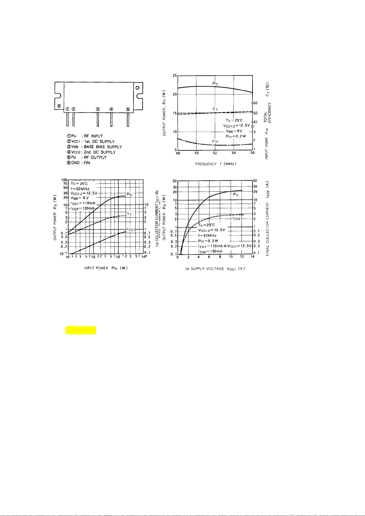
11) M57735 (XA0271)
50~54MHz
RF Power Module
Page 14
 Loading...