


DJ-G7E
DJ-G 7/T/E
Service Manual
CONTENTS
SPECIFICATIONS
General...................................................................2
Transmitter
Receiver.................................................................3
CIRCUIT DESCRIPTION
1) Reception.......................................................4-7
2) Transmission
3) CPU Peripheral.................................................7
4) CPU
SEMIC ONDUCTOR DATA
1) BU2152FS (XA0210)
2) NJM2070M (XA1352).....................................13
3) TA31136FN (XA0404)....................................13
4) TK10931V (XA0666)......................................13
5) M62364FP (XA1293).....................................14
6) TC3W53FU (XA0341)....................................14
7) MB15F07SL (XA1033)...................................15
8) UPC2771TB (XA0953)...................................15
9) UPC2757TB (XA0976)...................................15
10) AT24C1024B (XA1351)...............................15
11) BU4830FVE (XA1009).................................16
12) S-812C32AMC (XA1353).............................16
13) LM2681 (XA1354)
14) NJM2125F (XA0622)
15) TC75S51FU (XA1014)
16) LM12904PWR (XA1155)
17) NJM2746RB1 (XA1356)...............................17
18) BA2902FV (XA1371)....................................
19) MM1332EF (XA1139)
20) Transistor, Diode and LED Outline Drawings
21) LCD Connection (EL0063)...........................20
............................................................2
....................................................
..............................................................
.....................................12
........................................
...................................
.................................
..............................17
.................................
8-11
....
16
17
17
18
18
19
EXPLODED VIEW
1) Front View
2) Rear View
3) Bottom View
PARTS LIST
CPU Unit
7
MAIN Unit
VCO Unit
Mechanical Parts
LED Unit
JACK Unit
RE1 Unit
RE2 Unit
ADJUSTMENT
Adjustment Mode
PC BOARD VIEW
CPU Unit Side A
CPU Unit Side B
MAIN Unit Side A
MAIN Unit SideB
VCO Unit
JACK Unit............................
LED Unit..............................
RE Unit................................
SCHEMATIC DIAGRAM
BLOCK DIAGRAM.
.......................
........................
....................
.............................
............................
.............................
.................
..............................
............................
..............................
..............................
................
..................
..................
................
................
.............................
ALINCO Inc
ALINCO, INC
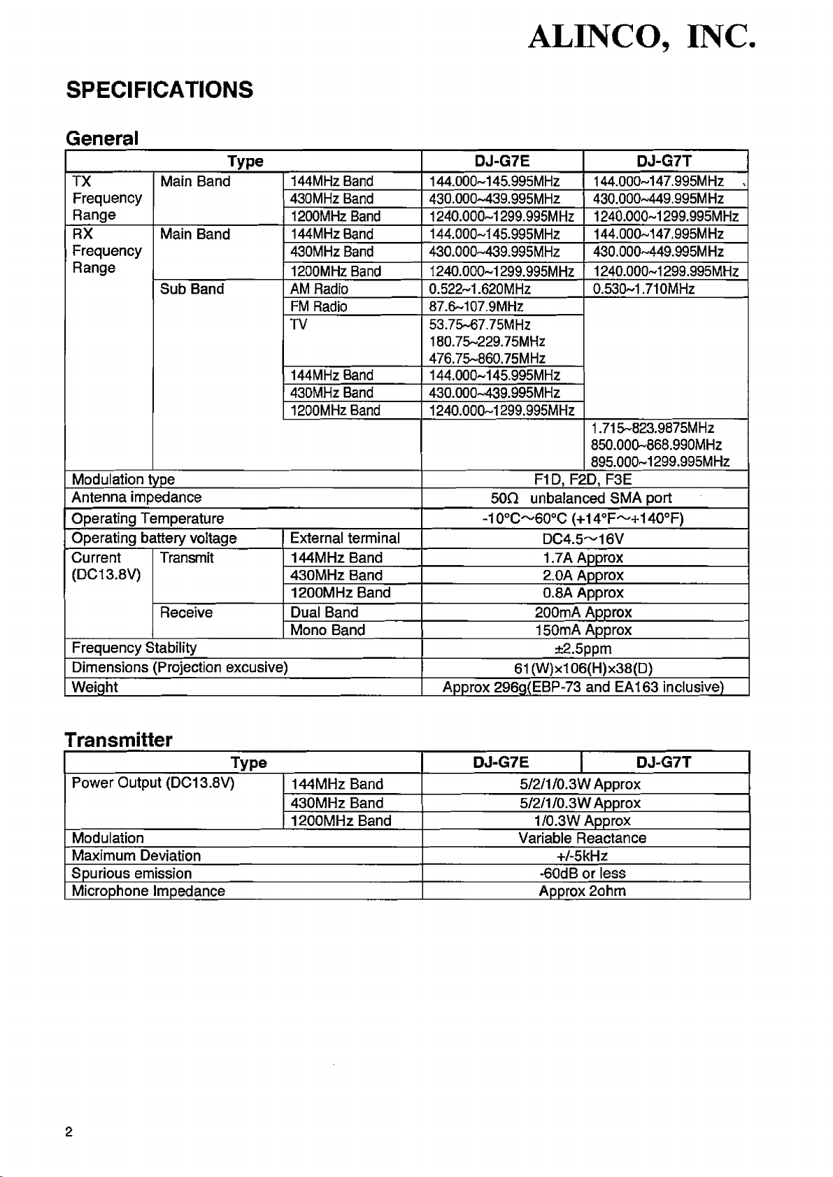
SPECIFICATIONS
General
Type
TX
Frequency
Range
RX
Frequency
Range
Modulation type
Antenna impedance
Operating Temperature -10°C~60°C (+14°F~+140°F)
Operating battery voltage
Current
(DC13.8V)
Frequency Stability
Dimensions (Projection excusive)
Weight
Main Band 144MHz Band 144.000-145.995MHz
430MHz Band
1200MHz Band
Main Band
Sub Band AM Radio
Transmit
Receive Dual Band 200mA Approx
144MHz Band
430MHz Band
1200MHz Band
FM Radio
TV
144MHz Band 144.000-145.995MHz
430MHz Band
1200MHz Band
External terminal
144MHz Band 1.7A Approx
430MHz Band 2.0A Approx
1200MHz Band 0.8A Approx
Mono Band
430.000-439.995MHz 430.000-449.995M Hz
1240.000-1299.995MHz 1240.000-1299.995MHz
144.000-145.995MHz
430.000-439.995MHZ
1240.000-1299.995MHz 1240.000-1299.995MHz
0.522-1.620MHz
87.6-107.9MHz
53.75-67.75MHZ
180.75-229.75MHZ
476.75~860.75MHz
430.000-439.995MHz
1240.000-1299.995MHz
DJ-G7E DJ-G7T
144.000-147.995M Hz ,
144.000-147.995MHZ
430.000-449.995M Hz
0.530-1.710MHz
1.715-823.9875MHZ
850.000-868.990MHZ
895.000-1299.995MHz
F1D, F2D, F3E
500 unbalanced SMA port
DC4.5~16V
150mA Approx
±2.5ppm
61 (W)x106(H)x38(D)
Approx 296g(EBP-73 and EA163 inclusive)
Transmitter
Power Output (DC13.8V)
Modulation
Maximum Deviation
Spurious emission
Microphone Impedance
2
Type
DJ-G7E DJ-G7T
144MHz Band 5/2/1/0.3W Approx
430MHz Band
1200MHz Band
5/2/1/0.3W Approx
1/0.3W Approx
Variable Reactance
+/-5kHz
-60dB or less
Approx 2ohm
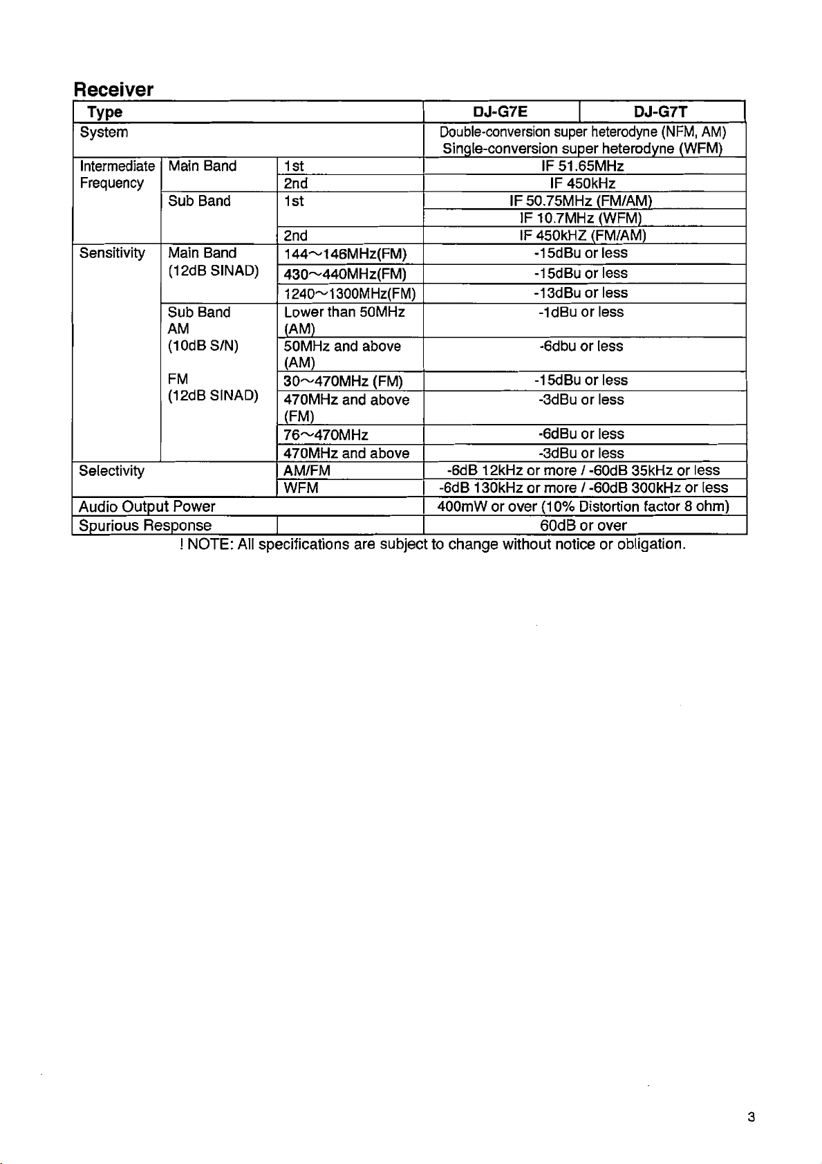
Receiver
Type
System
Intermediate
Frequency
Sensitivity
Selectivity AM/FM
Audio Output Power
Spurious Response 60dB or over
Main Band 1st IF 51.65MHz
2nd IF 450kHz
Sub Band 1st IF 50,75MHz (FM/AM)
2nd
Main Band
(12dB SINAD)
Sub Band
AM
(10dB S/N)
FM
(12dB SINAD)
! NOTE: All specifications are subjec
144—146MHz(FM)
430~440MHz(FM)
1240~1300MHz(FM)
Lower than 50MHz
(AM)
50MHz and above
(AM)
30~470MHz (FM)
470MHz and above
(FM) .
76^470MHz
470MHz and above -3dBu or less
WFM
to change without notice or obligation.
DJ-G7E DJ-G7T
Double-conversion super heterodyne (NFM, AM)
Sinqle-conversion super heterodyne (WFM)
IF 10.7MHz (WFM)
IF 450kHZ (FM/AM)
-15dBu or less
-15dBu or less
-13dBu or less
-1dBu or less
-6dbu or less
-15dBu or less
-3dBu or less
-6dBu or less
-6dB 12kHz or more / -60dB 35kHz or less
-6dB 130kHz or more / -60dB 300kHz or less
400mW or over (10% Distortion factor 8 ohm)
3
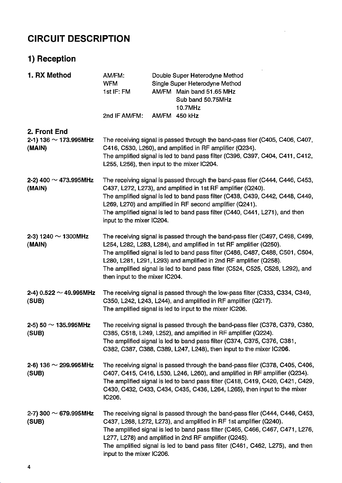
CIRCUIT DESCRIPTION
1) Reception
1. RX Method
2. Front End
2-1) 136 ~ 173.995MHz
(MAIN)
2-2) 400 ~ 473.995MHz
(MAIN)
2-3) 1240 — 1300MHz
(MAIN)
AM/FM: Double Super Heterodyne Method
WFM Single Super Heterodyne Method
1st IF: FM AM/FM Main band 51.65 MHz
Sub band 50.75MHz
10.7MHz
2nd IF AM/FM: AM/FM 450 kHz
The receiving signal is passed through the band-pass filer (C405, C406, C407,
C416, C530, L260), and amplified in RF amplifier (Q234).
The amplified signal is led to band pass filter (C396, C397, C404, C411, C412,
L255, L256), then input to the mixer IC204.
The receiving signal is passed through the band-pass filer (C444, C446, C453,
C437, L272, L273), and amplified in 1st RF amplifier (Q240).
The amplified signal is led to band pass filter (C438, C439, C442, C448, C449,
L269, L270) and amplified in RF second amplifier (Q241).
The amplified signal is led to band pass filter (C440, C441, L271), and then
input to the mixer IC204.
The receiving signal is passed through the band-pass filer (C497, C498, C499,
L254, L282, L283, L284), and amplified in 1st RF amplifier (Q250).
The amplified signal is led to band pass filter (C486, C487, C488, C501, C504,
L280, L281, L291, L293) and amplified in 2nd RF amplifier (Q258).
The amplified signal is led to band pass filter (C524, C525, C526, L292), and
then input to the mixer IC204.
2-4) 0.522 ~ 49.995MHz
(SUB)
2-5) 50 ~ 135.995MHz
(SUB)
2-6) 136 — 299.995MHz
(SUB)
2-7) 300 ~ 679.995MHz
(SUB)
The receiving signal is passed through the low-pass filter (C333, C334, C349,
C350, L242, L243, L244), and amplified in RF amplifier (Q217).
The amplified signal is led to input to the mixer IC206.
The receiving signal is passed through the band-pass filer (C378, C379, C380,
C385, C518, L249, L252), and amplified in RF amplifier (Q224).
The amplified signal is led to band pass filter (C374, C375, C376, C381,
C382, 0387, C388, C389, L247, L248), then input to the mixer 1C206.
The receiving signal is passed through the band-pass filer (C378, C405, C406,
C407, C415, C416, L530, L246, L260), and amplified in RF amplifier (Q234).
The amplified signal is led to band pass filter (C418, C419, C420, C421, C429,
C430, C432, C433, C434, C435, C436, L264, L265), then input to the mixer
IC206.
The receiving signal is passed through the band-pass filer (C444, C446, C453,
C437, L268, L272, L273), and amplified in RF 1st amplifier (Q240).
The amplified signal is led to band pass filter (C465, C466, C467, C471, L276,
L277, L278) and amplified in 2nd RF amplifier (Q245).
The amplified signal is led to band pass filter (C461, C462, L275), and then
input to the mixer 1C206.
4

2-8) 680 ~ 1300MHz
(SUB)
The receiving signal is passed through the band-pass filer (C497, C498, C499,
L254, L282, L283, L284), and amplified in RF 1st amplifier (Q250).
The amplified signal is led to band pass filter (C508, C509, C510, L287, L288),
and amplified in RF second amplifier (Q256).
The amplified signal is led to band pass filter (C511, C512, C513, L286, L290),
and then input to the mixer IC206.
3.ATT
4 Mixer
4-1) Main Mixer
(FM/NFM)
4-2) Sub Mixer
(AM/FM)
4-2) Sub Mixer
(WFM)
This circuit is used in case the receiving signal is disturbed by interfering signal,
attenuating the receiving signal to reduce the interference. CPU (IC3) pin 30,
31 and 32 outputs a DC voltage to drive IC14, then ATTV on MAIN unit control
ling D207, D236 and D242. The serial resistor with diodes adjusted the attenu
ation value.
The input signal to the mixer IC204 and the 1 st local signal are added or, then
it is amplified at the 1st IF amplifier Q216 after the adjacent signal subtracted
at mixer IC204, and the crystal filter XF201 selects the signal of 51.65MHz is
eliminated.
The input signal to the mixer IC206 and the 1st local signal are added or, then
it is amplified at the 1st IF amplifier Q225 after the adjacent signal subtracted
at mixer IC206, and the crystal filter XF202 selects the signal of 50.75MHz is
eliminated.
The input signal to the mixer IC206 and the 1st local signal are added or, then
it is amplified at the 1st IF amplifier Q235 after the adjacent signal subtracted
at mixer IC206, and the crystal filter FL202 selects the signal of 10.7MHz is
eliminated.
5. IF
5-1) Main IF
5-2) Sub IF
5-3) Sub IF
(AM)
The signal amplified at the 1st IF amplifier Q216 is supplied to pin 16 of IC205
for demodulation. Also the signal of 12.8MHz pass through Q213 and Q214
and 51.2MHz (12.8MHz X 4) led to pin 1 of IC205.
2 input signals on pin 16 and 1, are mixed in the mixer circuit inside IC205 and
converted into the 2nd IF signal of 450kHz.The converted 2nd IF signal is
output from pin 3 of IC205.
The output signal from pin 3 of IC205 is led to pin 5 of IC205 after eliminating
the adjacent channel signal at the ceramic filter FL201. The input 2nd IF signal
to pin 5 of IC205 is demodulated at the limiter amplifier and quartered detector
circuits inside of IC205, then output from pin 9 of IC205 as an AF signal.
The signal amplified at the 1st IF amplifier Q225 is supplied to pin 24 of IC208
for demodulation. Also the signal of 12.8MHz pass through Q213 and Q214
and 51.2MHz (12.8MHz X4) led to pin 1 of 1C208.
2 input signals are mixed in the mixer circuit inside 1C208 and converted into
the 2nd IF signal of 450kHz. The converted 2nd IF signal is output from pin 3
of IC208.
The output signal from pin 3 of IC208 is led to pin 5 of IC208 after eliminating
the adjacent channel signal at the ceramic filter FL203. The input 2nd IF signal
to pin 5 of IC208 is demodulated at the limiter amplifier and quartered detector
circuits inside of IC208, then output from pin 13 of IC208 as AMAF signal.
5
5-4) Sub IF
(FM)
The output signal from pin 3 of IC208 is led to pin 7 of IC208 after eliminating
the adjacent channel signal at the ceramic filter FL204. The input 2nd IF signal
to pin 5 of IC208 is demodulated at the limiter amplifier and quartered detector
circuits inside of IC208, then output from pin 12 of IC208 as FMAF signal.
6-1) Main Squelch
6-2) Sub Squelch
7. Audio
8-1) Main VCO
The AF signal got from pin 9 of IC205 is fed to pin 8 of IC205. The input signal
is output from pin 14 of IC205 passing through the noise filter amplifier and
rectifier circuits inside of IC205. The rectified signal (MSQL) is added to the A/D
(Pin108) port of the microcomputer IC3. Judging the signal, the microcomputer
controls ON/OFF of the audio output (Pin68).
The AF signal got from pin 12 of IC208 is fed to pin 19 of IC208. The input
signal is output from pin 21 of IC208 passing through the noise filter amplifier
and rectifier circuits inside of IC208, The rectified signal is added to the A/D
port of the microcomputer IC3. Judging the signal, the microcomputer controls
ON/OFF of the audio output.
The all AF signals are attracted to the 1C10 on the CPU unit.
The volume of output audio signal is adjusted at the volume IC10 and the AF
amplifier Q7. And then the signal is input to pin 2 of audio power amplifier IC5
to output pass through the audio SW Q12 from pin 6 to drive a speaker, etc.
The Main VCO on oscillating frequency buffer amplifier Q602, oscillated signal
is supplied to pin 4 of PLL-IC202 passing through the buffer amplifier Q201.
The VCO in VHF band consists of the Colpitts oscillator. D601, D602, D603
and L601 determine the oscillating frequency, and the signal is oscillated at the
transistor Q601.
The VCO in UHF band consists of the Colpitts oscillator. D604, D605, D606
and L602 determine the oscillating frequency, and the signal is oscillated at the
transistor Q603.
The VCO in 1200MHz band consists of the Colpitts oscillator. D607, D608,
D609 and L603 determine the oscillating frequency, and the signal is oscillated
at the transistor Q604.
8-2) Sub VCO
6
The Sub VCO on oscillating frequency buffer amplifier Q702, oscillated signal
is supplied to pin 13 of PLL-IC202.
The VCO in 50MHz band consists of the Colpitts oscillator. D701, D703, and
L701, L702 determine the oscillating frequency, and the signal is oscillated at
the transistor Q701, The frequency shifts to VCO when Q703 is turned ON.
The VCO in VHF band consists of the Colpitts oscillator. D704, D706 and L703,
L704 determine the oscillating frequency, and the signal is oscillated at the
transistor Q704, The frequency shifts to VCO when Q705 is turned ON.
The VCO in UHF band consists of the Colpitts oscillator. D707, D709 and L705
determine the oscillating frequency, and the signal is oscillated at the
transistor Q706.
9. PLL
2) Transmission
1. Microphone Amplifier
PLL-IC202 is used to control the oscillating frequency of the VCO.
IC202 is controlled by the serial control signal (DATA, CLK, STB1) sent from
the microprocessor IC3. The 12.8MHz reference frequency of IC202, supplied
from crystal oscillator X201.
IC202 compares the frequency gained by dividing the signal added to pin 16 of
IC3 by the control signal from IC3 with the frequency gained by dividing the
reference frequency 12.8MHz. When the phase difference is found as a result
of phase comparison, the pulse signal is output from the charge pump output
of pin 8 (Main band) and pin 9 (Sub band) of IC202, then the signal is converted
into the DC voltage at the passive filter and added to the cathode side of the
VCO vari-cap D601, D603, D604, D606, D607, D609, D701, D703, D704,
D706, D707 and D709 to make the phases equal. In result the stabilized oscil
lation can be done at the desired frequency.
The audio signal is converted to a mute switch (Q20) and microphone gain
(Q24) Electric signal in either the internal or external microphone pass through
and two operational amplifiers, then supplied to IC10.
The voice is converted into the electric signal through the microphone, and
then supplied to IC10.
The input signal is amplified and pre-emphasized to be output.
The signal output from microphone amplifier is adjusted the maximum
frequency deviation at IC10. The adjusted signal is added to the cathode of the
VCO vari-cap D602 and D605 for deviation to change the capacity of the oscil
lation circuit resulting the FM deviation.
2. Power Amplifier
3) CPU Peripheral
I.Lamp
2.Tone/DCS/DTMF
Encoder
The VCO in VHF or UHF band oscillated signal of the VCO is supplied to the
power amplifier Q202, passing through buffer amplifier Q602 on VCO unit and
then pre-driver amplifier IC201, driver amplifier Q203. The power-amplified
signal is supplied to the antenna through the duplexer after the harmonics are
attenuated enough.
The VCO in 1200MHxz band oscillated signal of the VCO is supplied to the
power amplifier Q210, passing through buffer amplifier Q602 on VCO unit then
pre-driver amplifier IC201, driver amplifier Q212. The power-amplified signal is
supplied to the antenna through the duplexer after the harmonics are attenu
ated enough.
The CPU pin 117, 118 and 119 outputs a DC voltage to drive IC6, controls.
The brightness of the lamp can be adjusted by five stages lamp lights when
operating
Lamp (D4, D5, D6, D7, D8, D9, D801, D802) lights when ten keys are operated.
The lamp outputs by five stages and adjusts the DC current with CPU pin 117,
118 and 119 to IC6.
The CPU pin 7 is equipped with an internal tone/DCS/DTMF encoder.
The tone signal (67.0 to 250.3Hz) is output.
The DCS code (023 to 754) is output
The DTMF code (1 to D) is output.
3. Tone/DCS Decoder
The AF signal from the IC205 or IC208 is filtered by an active filter (IC2) signal
amplified and input to pin 121 of the CPU
7
4) CPU
M30625FG (XA13871XA1388)
Terminal Connection
(TOP VIEW)
« « xf i
6 6 6
_ e e e e e
W W t «5 © N
i i i i
c j ej
evj1 cJ w
z z
z z z
i s <
s^ai1
Q- Q- CL CL CL
Ci y- f- y-
eeee
»- c Q m *
Jill
¿ . C L .K .C L
cn pr \to ^
N N M ,
" e e i
in <o
e q
(D Is -
FT
<3. Is*.
e
I I
CJ OJ
I I
« w o - ,« « s i i s i i 5 s s s ’y 'y 'y ^
SSg
«' cJ « i c J c J n ” , 10,<0I ^ 3 j 5 3 j 2 3 s
Q. > C L C L C L C L C L C L C L Q .C L Q . C L C L C LO - O .Q . D -C L C L C L
P1_0/D8
PO_7/ANO_7/D7
PO_6/ANO_6/D6
PO_5/ANO_5/D5
P0_4/AN0_4/D4
PO_3/ANO_3/D3
PO_2/ANO_2/D2
P0„1/AN0_1/D1
P0„O/AN0_0/D0
P11_7
P11_6
P11_5
P11_4 ■
P11_3 ■
P11_2 ■
P11_1
P11_0
P10_7/AN7/ffi3 •
P10_6/AN6/KI2 ■
P10_5/AN5/KI1
P10_4/AN4/Kl0
P10.3/AN3
P10_2/AN2 ■
P10.1/AN1
AVSS
PIOO/ANO
O
o
o
tu m m m T m n m u m tm m m u
J D. 0.
P12_5
P12_6
P12_7 _
P5_0/WRL/WR
P5_1/WRH/BHE
P5_2/RD
P5_3/BCLK
P13_0
P13_1
P13_2
P13_3
P5_4/HLDA
P5_5/HOLO
P5_6/ALE
P5_7/RDY/CLKOUT
P13_4
P13_5
P13_6
P 1 3 _ 7
P6_0/CT50/RT SO
P6.1/CLK0
P6.2/FIXOO/SCLO
Pg_3/TXD0/SDA0
P6„4/CTS 1 /RTS1 /CTSO/CLKS1
P6_5/CLK1
VSS
____
____
8
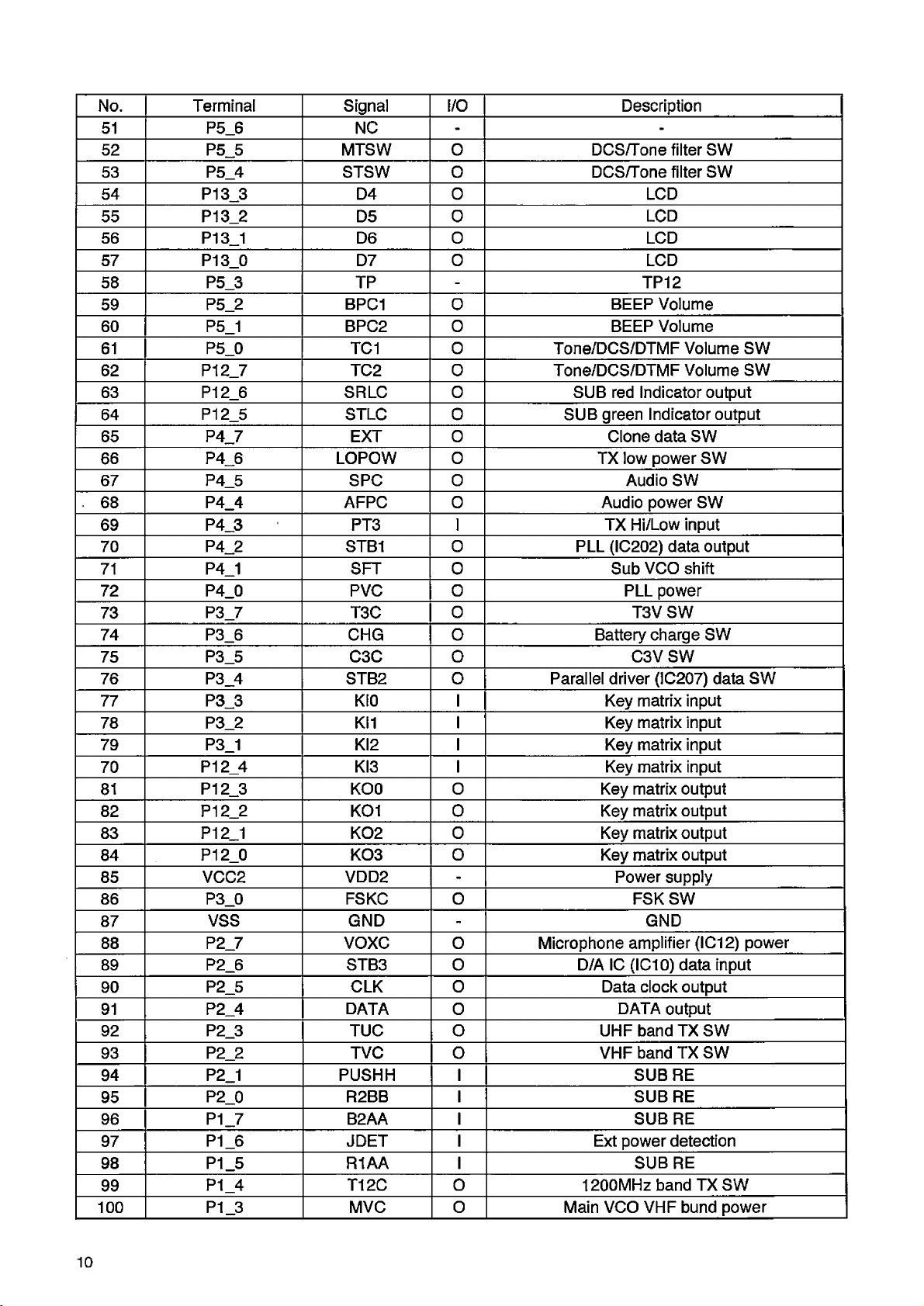
No. Terminal
1 VREF VDD2
2 AVCC
3 P9_7 DCSW
4 P9_6
5
P9_5 TDC
6 P9_4
7
P9_3
8 P9_2
9
10
11
P9_1
P9_0
P14_1
12 P14_0 SDATA
13 BATE GND
14
CNVSS
15 P8_7 TFSK 0
16
P8__6
Signal I/O Description
VDD2
MUTE
TRKV
TDD
MSW
XBR
-
-
0
0 Mute
0
0 Front End control
I
o Cross Band Repeater SW
Power supply
Power supply
DCS mute SW
Tone mute SW
Tone/DCS/DTMF output
MONI SW
DTSW o Tone/DCS/DTMF SW
SCLK
GND
-
-
- GND
-
Signal clock for EEPROM
Signal data for EEPROM
GND
FSK output
XSW 0 Clock shift output
17 RESET RST I Reset input
18
XOUT
XOUT 0
19 VSS GND
20
21
XIN
VCC1
XIN I
VDD
22 P8_5 VDS
23
24
P8_4
RFSK I
P8_3 R1A I MAIN RE
-
-
-
Main clock output
GND
Main clock input
Power supply
Power supply
FSK input
25 P8_2 R2A I MAIN RE
26 P8_1
27
P8_0 BEEP
R1B I
o
MAIN RE
BEEP output
28 P7_7 R2B I MAIN RE
29 P7_6
TBST
30 P7_5 ATT1
31 P7_4
32
P7_3
ATT2
ATT3 o
o
o
o
Tone-burst output
ATT control output
ATT control output
ATT control output
33 P7_2 PUSH I MAIN RE
34 RSD2/SCL2 RXD I
35
TXD2/SDA2
36 P6_7
TXD o
MRLC
37 VCC1 VDD
0
- Power supply
Clone data input
Clone data output
MAIN red Indicator output
38 P6_6 MTLC o MAIN green Indicator output
39 VSS
40
41
P6_5
P6_4
GND
/CS1 o
/RES o
-
GND
LCD
LCD
42 P6_3 AO o LCD
43
44
P6_2
P6_1
WR o
/RD
45 P6_0 NC
46
P13_7
DO o
O
-
LCD
LCD
-
LCD
47 P13_6 D1 o LCD
48 P13_5 D2
49 P13_4
50 P5_7
D3 o LCD
RDCSW
o
o DCS/Tone filter shift
LCD
9
No. Terminal Signal I/O Description
51 P5_6 NC
- -
52 P5_5 MTSW o DCS/Tone filter SW
53 P5_4 STSW o DCS/Tone filter SW
54 P13_3 D4 0 LCD
55 P13_2 D5 0
LCD
56 P13_1 D6 0 LCD
57 P13_0 D7 0 LCD
58 P5_3 TP
59
P5_2
BPC1 0
-
TP12
BEEP Volume
60 P5_1 BPC2 0 BEEP Volume
61
P5_0 TC1 0 Tone/DCS/DTMF Volume SW
62 P12_7 TC2 0 Tone/DCS/DTMF Volume SW
63 P12_6 SRLC 0 SUB red Indicator output
64 P12_5 STLC 0
SUB green Indicator output
65 P4_7 EXT 0 Clone data SW
66
P4_6
LOPOW 0 TX low power SW
67 P4_5 SPC 0 Audio SW
. 68 P4_4 AFPC 0 Audio power SW
69 P4_3 PT3 I
TX Hi/Low input
70 P4_2 STB1 0 PLL (IC202) data output
71 P4_1 SFT 0
72 P4_0 PVC
73
P3_7
T3C
O
0 T3V SW
Sub VCO shift
PLL power
74 P3_6 CHG o Battery charge SW
75
P3_5 C3C o C3V SW
76 P3_4 STB2 0 Parallel driver (1C207) data SW
77 P3_3 KIO I Key matrix input
78 P3_2 KI1 I
Key matrix input
79 P3_1 KI2 I Key matrix input
70
81
82
P12_4 KI3 I Key matrix input
P12_3 KOO 0 Key matrix output
P12_2
K01 0
Key matrix output
83 P12_1 K02 0 Key matrix output
84
85 VCC2 VDD2
P12_0 K03 o Key matrix output
-
Power supply
86 P3_0 FSKC o FSK SW
87
VSS GND
88 P2_7 VOXC o
-
GND
Microphone amplifier (IC12) power
89 P2_6 STB3 o D/A IC (IC10) data input
90
91 P2_4 DATA 0
P2_5 CLK 0 Data clock output
DATA output
92 P2_3 TUC o UHF band TX SW
93 P2_2 TVC o
VHF band TX SW
94 P2_1 PUSHH I SUB RE
95 P2_0
96 P1_7 B2AA I
97
P1_6 JDET I Ext power detection
98 P1_5 R1AA I
99
P1_4 T12C 0 1200MHz band TX SW
R2BB I SUB RE
SUB RE
SUB RE
100 P1_3 MVC 0 Main VCO VHF bund power
10
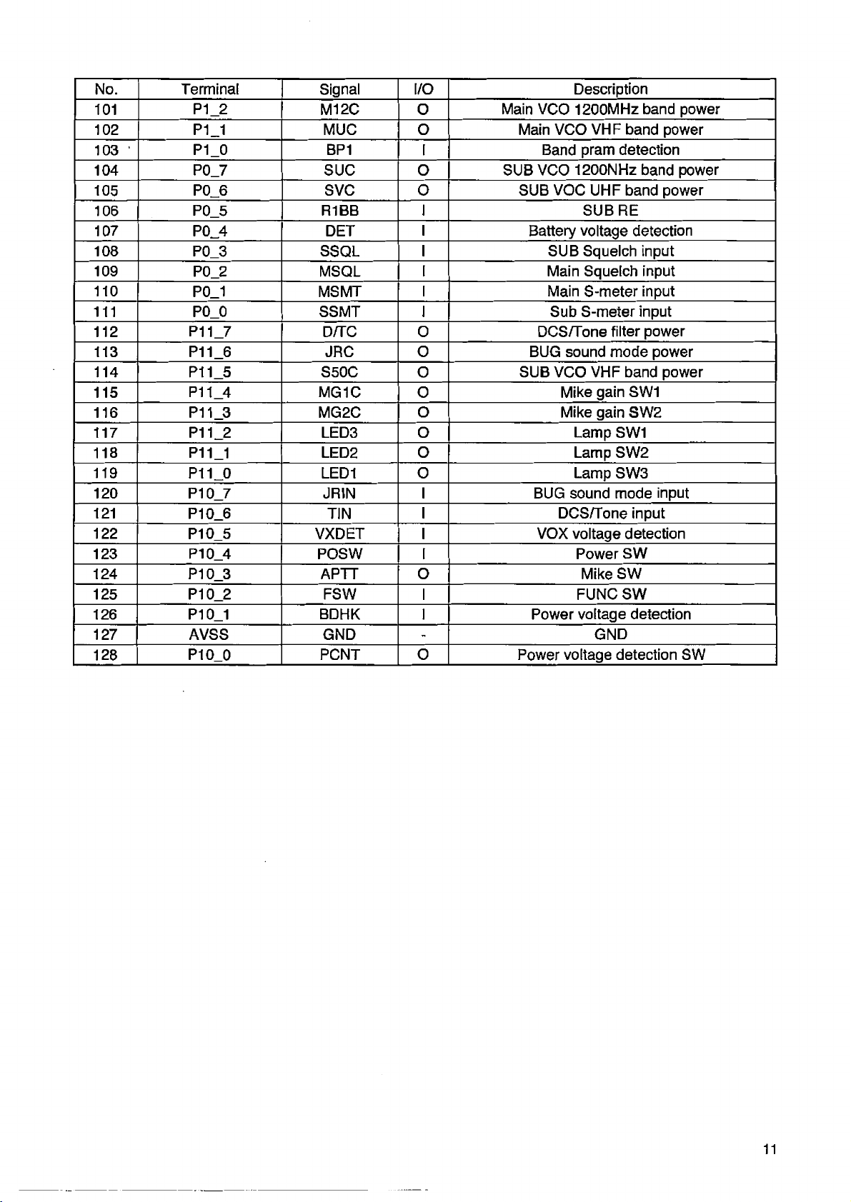
No. Terminal Signal I/O Description
101
102
103 '
104 P0_7 sue o
105
106 P0_5
107
108
109
110
111 P0_0 SSMT I
112
113 P11_6 JRC o BUG sound mode power
114
115 P11_4 MG1C o
116 P11_3 MG2C
117 P11_2 LED3 o Lamp SW1
118
119 P11_0 LED1 o Lamp SW3
120 P10_7
121 P10_6
122 P10_5 VXDET
123 P10_4 POSW I Power SW
124 P10_3 APTT o
125
126 P10_1 BDHK ]
127 AVSS GND
128 P10_0
P1_2
P1_1
P1_0 BP1
P0_6 SVC 0 SUB VOCUHF band power
P0_4 DET
P0_3 SSQL
P0_2 MSQL
P0_1
P11_7
P11_5
M12C O
MUC O Main VCO VHF band power
I
R1BB I SUB RE
I
I SUB Squelch input
I Main Squelch input
MSMT I
Df\C 0
S50C
o
o
P11_1
P10_2 FSW
LED2
JRIN
TIN
PCNT o Power voltage detection SW
o Lamp SW2
I BUG sound mode input
I
I
I
- GND
Main VCO 1200MHz band power
Band pram detection
SUB VCO 1200NHz band power
Battery voltage detection
Main S-meter input
Sub S-meter input
DCS/Tone filter power
SUB VCO VHF band power
Mike gain SW1
Mike gain SW2
DCS/Tone input
VOX voltage detection
Mike SW
FUNC SW
Power voltage detection
11
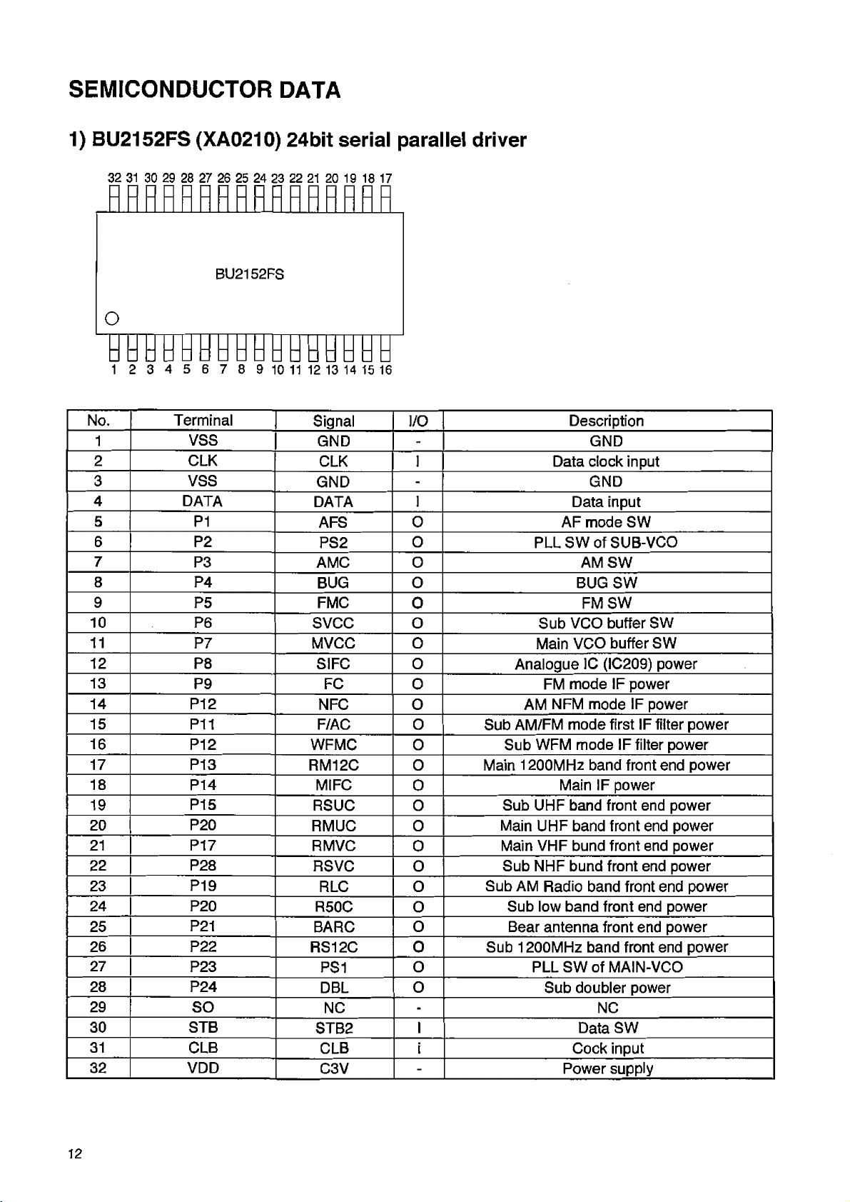
SEMICONDUCTOR DATA
1) BU2152FS (XA0210) 24bit serial parallel driver
32 31 30 29 28 27 26 25 24 23 22 21 20 19 18 17
No.
1
2 CLK
3 VSS
4
5 P1
6 P2
7
8 P4
9
10 P6
11
12 P8
13
14 P12
15
16 P12
17 P13
18 P14
19
20
21 P17
22 P28
23
24 P20
25
26
27
28 P24
29
30 STB
31 CLB
32 VDD
Terminal
VSS
DATA
P3
P5 FMC
P7 MVCC o
P9 FC
P11 F/AC 0 Sub AM/FM mode first IF filter power
P15
P20
P19
P21
P22
P23
SO
Signal I/O
GND
CLK 1 Data clock input
GND
DATA
AFS
PS2
AMC o AM SW
BUG o
-
-
1
0 AF mode SW
0
0
SVCC o
SIFC 0
Analogue 1C (IC209) power
0
NFC o
WFMC 0
RM12C 0 Main 1200MHz band front end power
MIFC
RSUC 0
RMUC 0 Main UHF band front end power
RM VC
RSVC o
RLC o Sub AM Radio band front end power
R50C o
BARC
RS12C 0 Sub 1200MHz band front end power
PS1
DBL 1
NC
STB2
CLB
C3V
0
0
o
o PLL SW of MAIN-VCO
o
-
1
i
-
AM NFM mode IF power
Sub WFM mode IF filter power
Sub UHF band front end power
Main VHF bund front end power
Sub NHF bund front end power
Sub low band front end power
Bear antenna front end power
Description
GND
GND
Data input
PLL SW of SUB-VCO
BUG SW
FM SW
Sub VCO buffer SW
Main VCO buffer SW
FM mode IF power
Main IF power
Sub doubler power
NC
Data SW
Cock input
Power supply
12
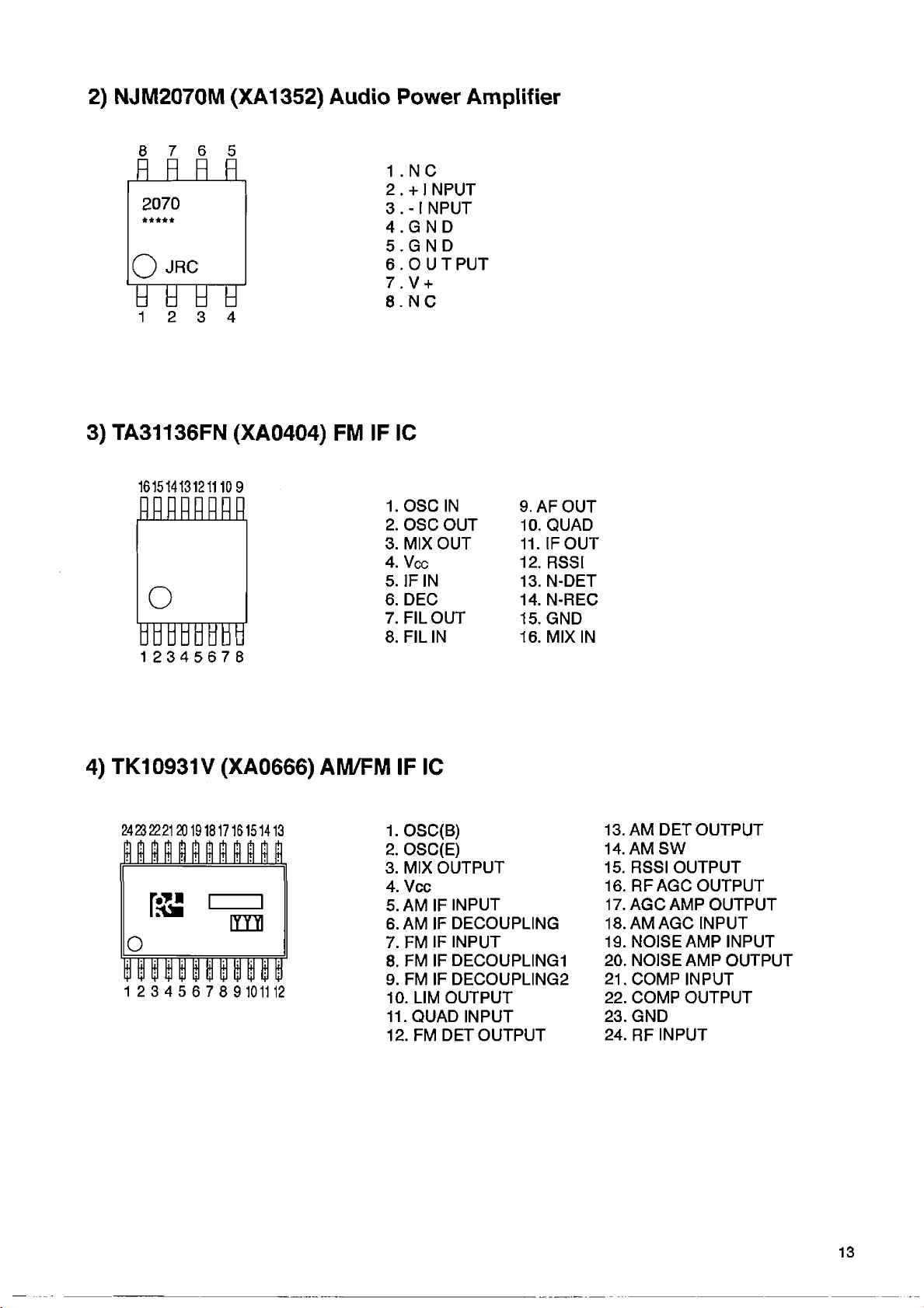
2) NJM2070M (XA1352) Audio Power Amplifier
6 7 6 5
R R R R
1 .NC
2.+INPUT
2070
* * * * *
O JRC
y y y y
3 . -1NPUT
4..G N D
. V
. N
D
+
C
5.,GN
6..0 U T PUT
7.
8.
3) TA31136FN (XA0404) FM IF IC
16151413121110 9
1 1 1 1
HtjUUHHÜH
12345678
I.O S C IN
2. OSC OUT
3. MIX OUT 11. IF OUT
4. Vcc
5. IFIN 13. N-DET
6. DEC
7. FIL OUT
8. FILIN 16. MIX IN
9. AF OUT
10. QUAD
12. RSSI
14. N-REC
15. GND
4) TK10931V (XA0666) AM/FM IF IC
242322212019181716151413 1. OSC(B)
2. OSC(E)
3. MIX OUTPUT
4. Vcc
5. AM IF INPUT
6. AM IF DECOUPLING
7. FM IF INPUT
8. FM IF DECOUPLING1
9. FM IF DECOUPLING2
10. LIM OUTPUT
11. QUAD INPUT
12. FM DET OUTPUT
13. AM DET OUTPUT
14. AM SW
15. RSSI OUTPUT
16. RFAGC OUTPUT
17. AGC AMP OUTPUT
18.AMAGC INPUT
19. NOISE AMP INPUT
20. NOISE AMP OUTPUT
21. COMP INPUT
22. COMP OUTPUT
23. GND
24. RF INPUT
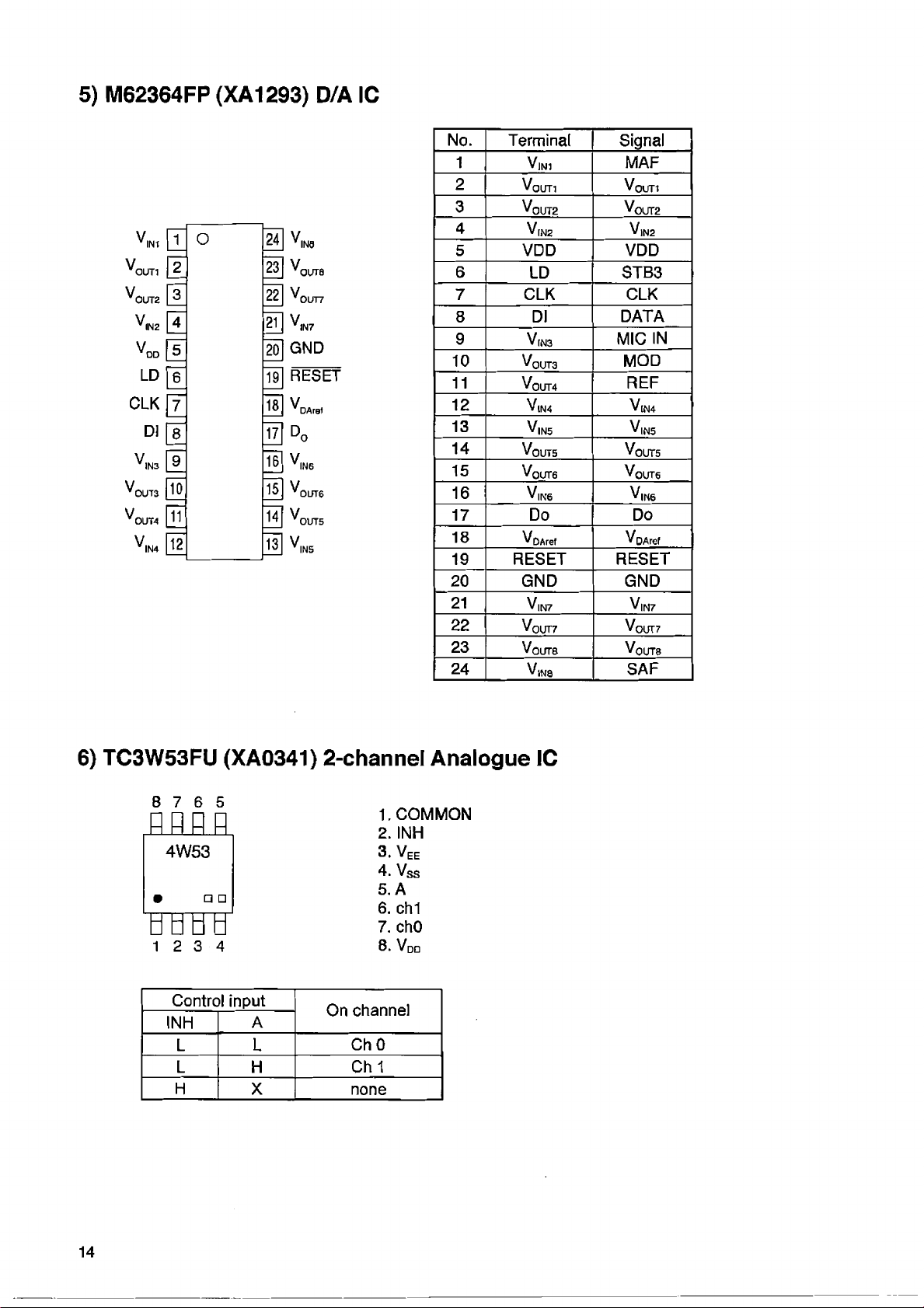
5) M62364FP (XA1293) D/A IC
v
V,
0UT1
V
0UT2
v„
v
CLK
V
ÛUT3
OUT4
v
INI
IN 2
OD
LD
Dl
IN3
IN4
O
1
2 23
~3
4
5 20
I*
7
_8
9
10 15
11 14
12 13
24
22
21
19
18
17
16
IN0
V,
oura
V,
OUT7
VlN7
GND
RESET
V,
DAref
IN6
OUT6
OUT5
IN5
No. Terminal Signal
1
2
3
4
5
6
vl N1
Vo U T1 VouTi
VoUT 2 Vout2
V|N2
VDD VDD
LD STB3
MAF
V,N2
7 CLK CLK
8 Dl
9
10
11 J
12
13
14
15
16
V|N3
VoU T3
VoUT 4
ViN4
V|N5
VoU T5 VoUT5
V0U T6
V|N6
17 Do
18
^DAre f
DATA
MIC IN
MOD
REF
V[N4
V|N5
V0UT 6
V|N6
Do
V QAr ef
19 RESET RESET
20 GND GND
21
22
23
24
V |N7
VoUT 7 VoUT 7
Vours
Vins
V |N7
V0UT 8
SAF
6) TC3W53FU (XA0341) 2-channel Analogue IC
8 7 6 5
nnnn
Control Input
INH
L L
L H
H X
A
On channel
1. COMMON
2. INH
3.V ee
4. Vss
5. A
6. ch1
7. chO
8. Vqq
ChO
Ch 1
none
14
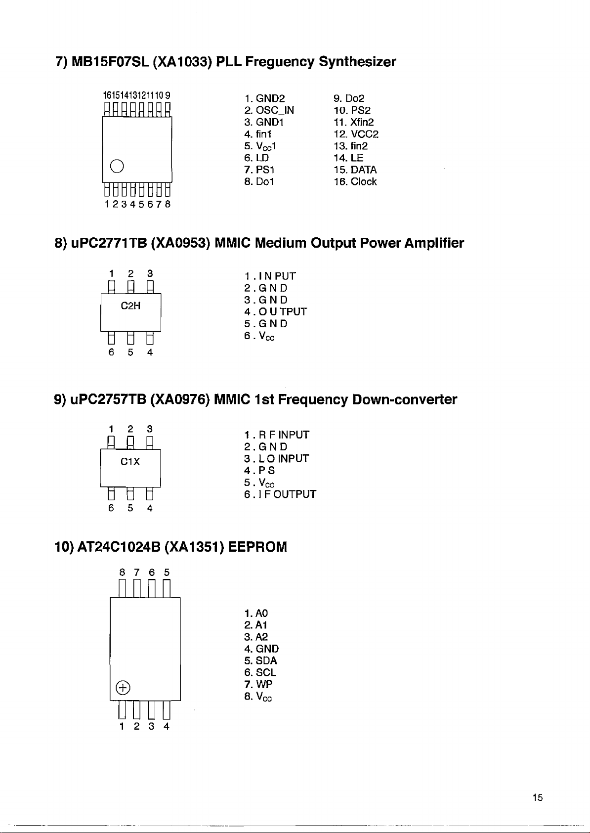
7) MB15F07SL (XA1033) PLL Freguency Synthesizer
161514131211109
M M M M
□ □ □ □ □ □ □ □
12 3 45678
1.GND2
2. OSC IN
3. GND1 11. Xfin2
4. fini 12. VCC2
5. Vcc1
6. LD
7. PS1
8. Do1 16. Clock
9. Do2
10. PS2
13. fin2
14. LE
15. DATA
8) uPC2771TB (XA0953) MMIC Medium Output Power Amplifier
1 2 3
n n n
C2H
6 5 4
1 . 1 N PUT
2.GND
3.GND
4 . O U TPUT
5.GND
6 . Vcc
9) uPC2757TB (XA0976) MMIC 1st Frequency Down-converter
1 2 3
non
C1X
6 5 4
1 . R F INPUT
2.GND
3. LO INPUT
4. PS
5. Vcc
6 . I F OUTPUT
10) AT24C1024B (XA1351) EEPROM
8 7 6 5
1. AO
2. A1
3. A2
4. GND
5. SDA
6. SCL
7. WP
8. V C c
15

11) BU4830FVE (XA1009) RESET IC
1. Vo UT
2. SUB
3. N.C.
4. V
dd
5. GND
Vdd su b
12) S-812C32AMC (XA1353) 3.2V Voltage Regulator
1. VlN
2. Vss
3. CE
4. NC
5. Voirr
d d d
1 2 3
13) LM2681 (XA1354) Switched capacitor voltage converter
6 5 4
□ □ □
S10A
1. V+
2. GND
3. CAP-
4. GND
5. OUT
6. CAP+
□ □ □
1 2 3
16
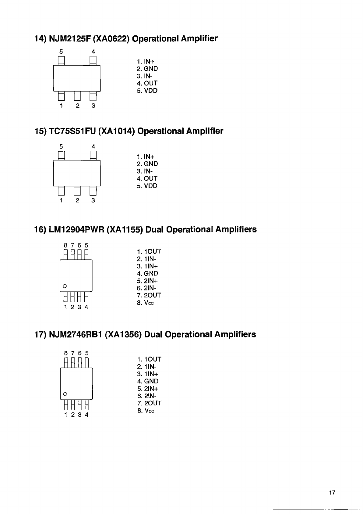
14) NJM2125F (XA0622) Operational Amplifier
1. IN+
2. GND
3. IN-
4. OUT
5. VDD
15) TC75S51FU (XA1014) Operational Amplifier
1. IN+
2. GND
3. IN-
4. OUT
5. VDD
16) LM12904PWR (XA1155) Dual Operational Amplifiers
8 7 6 5
RRRR
1 2 3 4
1. 10UT
2. 1IN-
3. 1IN+
4. GND
5. 2IN+
6. 2IN-
7. 20UT
8. Vcc
17) NJM2746RB1 (XA1356) Dual Operational Amplifiers
8 7 6 5
M R R
M¥H
12 3 4
1. 10UT
2.1IN-
3.1IN+
4. GND
5. 2IN+
6. 2lN-
7. 20UT
8. Vcc
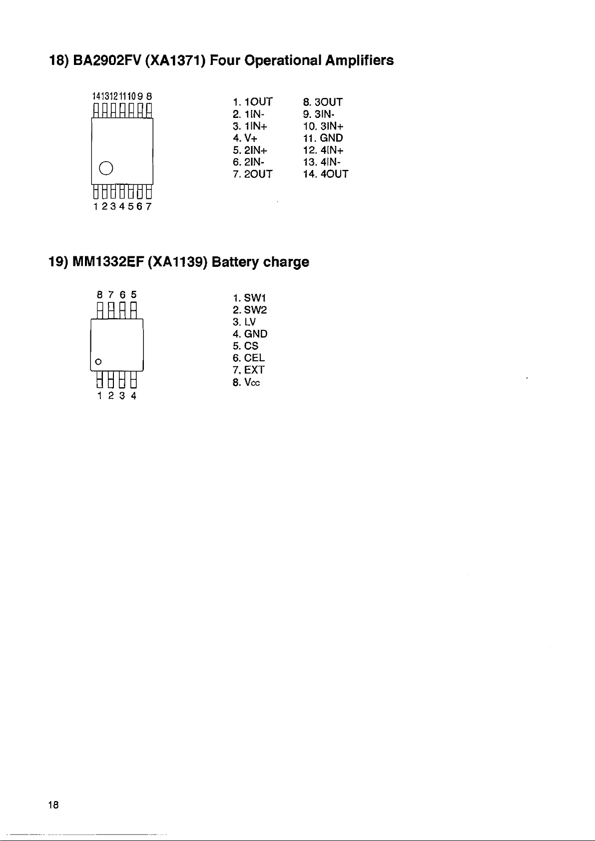
18) BA2902FV (XA1371) Four Operational Amplifiers
14131211109 8
w m m
1. 10UT
2. 1IN-
3. 1IN+
4. V+ 11. GND
5. 2IN+
6. 2IN- 13. 4IN-
7. 20UT 14. 40UT
ÏÏÏÏÏÏM ÏÏ
123456 7
19) MM1332EF (XA1139) Battery charge
8 7 6 5
RHRR
1.SW1
2. SW2
3. LV
4. GND
5. CS
6. CEL
7. EXT
8. Vcc
8. 30UT
9. SIN-
10. 3IN+
12. 4IN+
18
 Loading...