


 Loading...
POWER AMPLIFIER
ÉvÉäÉEÉXÉKÉCÉhÉuÉbÉN |
SERVICE MANUAL |
|
P5000S
P7000S
CONTENTS |
|
SPECIFICATIONS ........................................................ |
3/4 |
DIMENSIONS ..................................................................... |
5 |
PERFORMANCE GRAPHS ................................................ |
5 |
PANEL LAYOUT ............................................... |
6 |
CIRCUIT BOARD LAYOUT&WIRING |
|
..................................... |
8 |
DISASSEMBLY PROCEDURE ..................................... |
14 |
IC BLOCK DIAGRAM IC ........................................... |
21 |
CIRCUIT BOARDS ................................................ |
22 |
INSPECTION ........................................................................ |
35 |
PARTS LIST |
|
BLOCK DIAGRAM |
|
WIRING |
|
OVERALL CIRCUIT DIAGRAM |
|
PA 011698
P5000S: 200307-155000 P7000S: 200307-185000
HAMAMATSU, JAPAN
Copyright (c) Yamaha Corporation. All rights reserved. PDF-K368 
 03.08
03.08

P5000S / P7000S
IMPORTANT NOTICE
This manual has been provided for the use of authorized Yamaha Retailers and their service personnel. It has been assumed that basic service procedures inherent to the industry, and more specifically Yamaha Products, are already known and understood by the users, and have therefore not been restated.
WARNING: Failure to follow appropriate service and safety procedures when servicing this product may result in personal injury, destruction of expensive components and failure of the product to perform as specified. For these reasons, we advise all Yamaha product owners that all service required should be performed by an authorized Yamaha Retailer or the appointed service representative.
IMPORTANT: This presentation or sale of this manual to any individual or firm does not constitute authorization, certification, recognition of any applicable technical capabilities, or establish a principal-agent relationship of any form.
The data provided is believed to be accurate and applicable to the unit(s) indicated on the cover. The research engineering, and service departments of Yamaha are continually striving to improve Yamaha products. Modifications are, therefore, inevitable and changes in specification are subject to change without notice or obligation to retrofit. Should any discrepancy appear to exist, please contact the distributor's Service Division.
WARNING: Static discharges can destroy expensive components. Discharge any static electricity your body may have accumulated by grounding yourself to the ground bus in the unit (heavy gauge black wires connect to this bus).
IMPORTANT: Turn the unit OFF during disassembly and parts replacement. Recheck all work before you apply power to the unit.
WARNING: CHEMICAL CONTENT NOTICE!
The solder used in the production of this product contains LEAD. In addition, other electrical / electronic and / or plastic (where applicable) components may also contain traces of chemicals found by the California Health and Welfare Agency (and possibly other entities) to cause cancer and / or birth defects or other reproductive harm.
DO NOT PLACE SOLDER, ELECTRICAL / ELECTRONIC OR PLASTIC COMPONENTS IN YOUR MOUTH FOR ANY REASON WHAT SO EVER!
Avoid prolonged, unprotected contact between solder and your skin! When soldering, do not inhale solder fumes or expose eyes to solder / flux vapor!
If you come in contact with solder or components located inside the enclosure of this product, wash your hands before handling food.
IMPORTANT NOTICE FOR THE UNITED KINGDOM |
|
Connecting the Plug and Cord |
|
WARNING: THIS APPARATUS MUST BE EARTHED |
|
IMPORTANT. The wires in this mains lead are coloured in accordance |
|
with the following code: |
|
GREEN-AND-YELLOW : EARTH |
|
BLUE |
: NEUTRAL |
BROWN |
: LIVE |
As the colours of the wires in the mains lead of this apparatus may not |
|
correspond with the coloured markings identifying the terminals in |
|
your plug proceed as follows: |
|
The wire which is coloured GREEN-and-YELLOW must be connected |
|
to the terminal in the plug which is marked by the letter E or by the |
|
safety earth symbol |
or colored GREEN or GREEN-and-YELLOW. |
The wire which is coloured BLUE must be connected to the terminal |
|
which is marked with the letter N or coloured BLACK. |
|
The wire which is coloured BROWN must be connected to the termi-nal |
|
which is marked with the letter L or coloured RED. |
|
|
|
• This applies only to products distributed by Yamaha-Kemble Music (U.K.) Ltd. (3 wires) |
|
■ WARNING
Components having special characteristics are marked |
and must be replaced with parts having specification equal to those |
originally installed. |
|

2
P5000S /P7000S
■ SPECIFICATIONS
|
|
|
|
|
|
|
|
|
|
|
|
|
|
|
|
|
|
|
|
|
|
|
P5000S |
|
|
|
|
|
|
|
|
|
P7000S |
|
|||||
|
|
|
|
|
|
|
|
|
|
|
|
|
|
|
|
|
|
|
|
|
|
|
|
|
|
|
|||||||||||||
Power Output Level (Rated Power) |
8 Ω |
/STEREO |
|
|
|
|
|
|
|
|
|
525 W × |
2 |
|
|
|
|
|
|
|
|
750 W × |
2 |
|
|||||||||||||||
1 kHz |
|
|
|
4 Ω |
/STEREO |
|
|
|
|
|
|
|
|
|
750 W × |
2 |
|
|
|
|
|
|
|
|
1100 W × |
2 |
|
||||||||||||
THD + N = 1% |
8 Ω |
/BRIDGE |
|
|
|
|
|
|
|
1500 W × |
1 |
|
|
|
|
|
|
|
|
2200 W × |
1 |
|
|||||||||||||||||
|
|
|
|
8 Ω |
/STEREO |
|
|
|
|
|
|
|
|
|
500 W × |
2 |
|
|
|
|
|
|
|
|
700 W × |
2 |
|
||||||||||||
|
|
|
|
|
|
|
|
|
|
|
|
|
|
|
|
|
|||||||||||||||||||||||
|
|
|
|
|
|
|
|
|
|
|
|
|
|
|
|
|
|
|
|
|
|
|
|
|
|
|
|
|
|
|
|
|
|
|
650 W × 2 (European Model) |
|
|||
20 Hz |
|
20 kHz |
4 Ω |
/STEREO |
|
|
|
|
|
|
|
|
|
700 W × |
2 |
|
|
|
|
|
|
|
|
950 W × |
2 |
|
|||||||||||||
|
|
|
|
|
|
||||||||||||||||||||||||||||||||||
THD + N = 0.1% |
8 Ω |
/BRIDGE |
|
|
|
|
|
|
|
1400 W × |
1 |
|
|
|
|
|
|
|
|
1900 W × |
1 |
|
|||||||||||||||||
1 kHz |
|
|
|
2 Ω |
/STEREO |
|
|
|
|
|
|
|
1300 W × |
2 |
|
|
|
|
|
|
|
|
1600 W × |
2 |
|
||||||||||||||
|
|
|
|
|
|
|
|
|
|
|
|
|
|
|
|
||||||||||||||||||||||||
20 ms non-clip |
4 Ω |
/BRIDGE |
|
|
|
|
|
|
|
2600 W × |
1 |
|
|
|
|
|
|
|
|
3200 W × |
1 |
|
|||||||||||||||||
Power Bandwidth |
|
Half Power |
10 Hz |
|
|
40 kHz (THD + N = 0.5 %) |
|
|
|
|
|
|
|||||||||||||||||||||||||||
|
|
|
|
|
|||||||||||||||||||||||||||||||||||
|
|
|
|
|
|
|
|
|
|
|
|
|
|
|
|
|
|
|
|
|
|
|
|
|
|
|
|
|
|
|
|
||||||||
Total Harmonic Distortion (THD + N) |
4 Ω |
|
|
8 Ω /STEREO |
|
≤ |
0.1 % |
|
|
|
|
|
|
|
|
|
|
|
|
|
|
|
|
|
|
|
|||||||||||||
|
|
|
|
|
|
|
|
|
|
|
|
|
|
|
|
|
|
|
|
|
|
||||||||||||||||||
20 Hz |
|
20 kHz, Half Power |
8 Ω/BRIDGE |
|
|
|
|
|
|
|
|
|
|
|
|
|
|
|
|
|
|
|
|
||||||||||||||||
|
|
|
|
|
|
|
|
|
|
|
|
|
|
|
|
|
|
|
|||||||||||||||||||||
|
|
|
|
|
|
|
|
|
|
|
|
|
|
|
|
|
|
|
|
|
|
|
|
|
|
|
|
||||||||||||
Frequency Response |
RL = 8Ω , Po = 1 W |
0 dB, +0.5 dB, |
|
|
1 dB f = 20 Hz |
|
|
|
|
50 kHz |
|
|
|||||||||||||||||||||||||||
|
|
|
|
|
|
|
|||||||||||||||||||||||||||||||||
Intermodulation distortion (IMD) |
4 Ω |
|
|
8 Ω /STEREO |
|
≤ |
0.1 % |
|
|
|
|
|
|
|
|
|
|
|
|
|
|
|
|
|
|
|
|||||||||||||
|
|
|
|
|
|
|
|
|
|
|
|
|
|
|
|
|
|
|
|
|
|
||||||||||||||||||
60 Hz:7 kHz, 4:1, Half Power |
8 Ω |
/BRIDGE |
|
|
|
|
|
|
|
|
|
|
|
|
|
|
|
|
|
|
|
|
|||||||||||||||||
|
|
|
|
|
|
|
|
|
|
|
|
|
|
|
|
|
|
||||||||||||||||||||||
|
|
|
|
|
|
|
|
|
|
|
|
|
|
|
|
|
|
|
|
|
|
|
|
|
|
|
|||||||||||||
Channel Separation |
Half Power RL = 8 Ω 1 kHz |
|
≥ |
70 dB |
|
|
|
|
|
|
|
|
|
|
|
|
|
|
|
|
|
||||||||||||||||||
Vol. max |
|
input 600 Ω shunt |
|
|
|
|
|
|
|
|
|
|
|
|
|
|
|
|
|
|
|||||||||||||||||||
|
|
|
|
|
|
|
|
|
|
|
|
|
|
|
|
|
|
|
|||||||||||||||||||||
|
|
|
|
|
|
|
|
|
|
|
|
|
|
|
|
|
|
|
|
|
|
|
|
|
|
|
|
||||||||||||
|
|
|
|
|
|
|
|
|
|
|
|
|
|
|
|
|
|
|
|
|
|
|
|
|
|
|
|
|
|
|
|
||||||||
Residual Noise |
Vol. min. |
20 Hz |
|
|
|
|
20 kHz (DIN AUDIO) |
|
≤ |
|
|
70 dBu |
|
|
|
|
|
|
|
|
|
|
|
|
|
|
|
|
|
||||||||||
|
|
|
|
|
|
|
|
|
|
|
|
|
|
|
|
|
|
|
|
|
|
|
|||||||||||||||||
|
|
|
|
|
|
|
|
|
|
|
|
|
|
|
|
|
|
|
|
|
|
|
|
||||||||||||||||
SN Ratio |
|
|
|
20 Hz |
|
|
|
20 kHz (DIN AUDIO) |
|
|
|
|
|
|
|
|
|
|
|
103 dB |
|
|
|
|
|
|
|
|
|
104 dB |
|
||||||||
|
|
|
|
|
|
|
|
|
|
|
|
|
|
|
|
|
|
|
|
|
|
||||||||||||||||||
|
|
|
|
|
|
|
|
|
|
|
|
|
|
|
|
|
|
|
|
|
|
|
|
|
|
||||||||||||||
Damping Factor |
|
RL = 8 Ω , 1 kHz |
|
≥ |
350 |
|
|
|
|
|
|
|
|
|
|
|
|
|
|
|
|
|
|
|
|
||||||||||||||
|
|
|
|
|
|
|
|
|
|
|
|
|
|
|
|
|
|
|
|
|
|
||||||||||||||||||
|
|
|
|
|
|
|
|
|
|
|
|
|
|
|
|
|
|
|
|
|
|
|
|
|
|
|
|
|
|
|
|
|
|
|
|||||
Sensitivity (Vol. max.) Rated Power 8 Ω |
|
|
|
|
|
|
|
|
|
|
|
|
|
|
|
|
|
|
|
|
+6 dBu |
|
|
|
|
|
|
|
|
|
+8 dBu |
|
|||||||
Voltage Gain (Vol. max.) |
|
|
|
|
|
|
|
|
|
32.1 dB |
|
|
|
|
|
|
|
|
|
|
|
|
|
|
|
|
|
||||||||||||
|
|
|
|
|
|
|
|
|
|
|
|
|
|
|
|
|
|
|
|
|
|
|
|
|
|
||||||||||||||
Input Impedance |
|
|
|
|
|
|
|
|
|
|
30 kΩ |
/balanced, 15 kΩ |
/unbalanced |
|
|
||||||||||||||||||||||||
Controls |
|
|
|
Front Panel |
POWER switch (Push on/Push off) |
|
|
||||||||||||||||||||||||||||||||
|
|
|
|
|
|
|
|
|
|
|
|
|
Two 31-step Volume control knobs (one per ch) |
|
|
||||||||||||||||||||||||
|
|
|
|
|
|
|
|
|
|
|
|
|
|
|
|
|
|
||||||||||||||||||||||
|
|
|
|
Rear Panel |
MODE switch (STEREO/PARALLEL/BRIDGE) |
|
|
||||||||||||||||||||||||||||||||
|
|
|
|
|
|
|
|
|
|
|
|
|
Two FILTER switches (SUBWOOFER/LOW CUT/OFF) |
|
|
||||||||||||||||||||||||
|
|
|
|
|
|
|
|
|
|
|
|
|
Two fc knobs (25 to 150 Hz) |
|
|
|
|
|
|
|
|||||||||||||||||||
|
|
|
|
|
|
|
|
|
|
|
|
|
YS Processing switch (ON/OFF) |
|
|
|
|
|
|
|
|||||||||||||||||||
|
|
|
|
|
|
|
|
|
|
|
|
|
|
|
|
|
|
|
|
|
|
||||||||||||||||||
Connectors |
|
|
|
INPUT |
|
XLR-3-31 jacks (one per ch) |
|
|
|
|
|
|
|
||||||||||||||||||||||||||
|
|
|
|
|
|
|
|
|
|
|
|
|
1/4-inch TRS phone jacks (one per ch) |
|
|
||||||||||||||||||||||||
|
|
|
|
|
|
|
|
|
|
|
|
|
|
|
|
|
|
|
|
|
|||||||||||||||||||
|
|
|
|
OUTPUT |
Speakon jacks (one per ch) |
|
|
|
|
|
|
|
|||||||||||||||||||||||||||
|
|
|
|
|
|
|
|
|
|
|
|
|
5-way binding posts |
|
|
|
|
|
|
|
|
|
|
|
|
|
|
||||||||||||
|
|
|
|
|
|
|
|
|
|
|
|
|
1/4-inch phone jacks (one per ch) |
|
|
|
|
|
|
|
|||||||||||||||||||
|
|
|
|
|
|
|
|
|
|
|
|
|
|
|
|
|
|
|
|
|
|
|
|
|
|
|
|||||||||||||
Indicators |
|
|
|
POWER |
|
|
1 (Green) |
|
|
|
|
|
|
|
|
|
|
|
|
|
|
|
|
|
|||||||||||||||
|
|
|
|
PROTECTION |
|
|
1 (Red) |
|
|
|
|
|
|
|
|
|
|
|
|
|
|
|
|
|
|||||||||||||||
|
|
|
|
TEMP |
|
|
|
1 (Red) (heatsink temp |
≥ |
85 |
|
|
|
|
|
|
|
|
|
||||||||||||||||||||
|
|
|
|
|
|
|
|
|
|
|
|
|
|
|
|||||||||||||||||||||||||
|
|
|
|
CLIP |
|
|
|
2 (Red) |
|
|
|
|
|
|
|
|
|
|
|
|
|
|
|
|
|
||||||||||||||
|
|
|
|
SIGNAL |
|
|
|
2 (Green) |
|
|
|
|
|
|
|
|
|
|
|
|
|
|
|
|
|
||||||||||||||
|
|
|
|
YS Processing |
|
|
1 (Yellow) |
|
|
|
|
|
|
|
|
|
|
|
|
|
|
|
|
|
|||||||||||||||
|
|
|
|
|
|
|
|
|
|
|
|
|
|
|
|
|
|
|
|
|
|
|
|
|
|
|
|||||||||||||
Load protection |
|
|
|
|
|
|
|
|
|
|
POWER switch ON/OFF muting |
|
|
|
|
|
|
|
|||||||||||||||||||||
|
|
|
|
|
|
|
|
|
|
|
|
|
|
|
|
|
|
|
|
|
|
|
|
|
|
|
|
|
|
|
|
||||||||
|
|
|
|
|
|
|
|
|
|
|
|
|
DC-fault power supply |
|
|
|
|
|
|
|
|
|
|
|
|
|
|
||||||||||||
|
|
|
|
|
|
|
|
|
|
|
|
|
shutdown |
|
|
|
|
|
|
|
|
|
|
|
|
|
|
|
|
|
|||||||||
|
|
|
|
|
|
|
|
|
|
|
|
|
|
|
|
|
|
|
|
|
|
|
|
|
|||||||||||||||
Amp. protection |
|
|
|
|
|
|
|
|
|
|
Temp. detection (heat sink temp |
≥ |
|
90 VI limiter (RL |
≤ |
|
1Ω) |
|
|||||||||||||||||||||
|
|
|
|
|
|
|
|
|
|
|
|
||||||||||||||||||||||||||||
Limiter |
|
|
|
|
|
|
|
|
|
|
|
|
Comp: THD |
≥ |
|
0.5 % |
|
|
|
|
|
|
|
|
|
|
|
|
|
|
|||||||||
|
|
|
|
|
|
|
|
|
|
|
|
|
|
|
|
|
|
|
|
|
|
|
|
|
|
|
|||||||||||||
|
|
|
|
|
|
|
|
|
|
|
|
|
|
|
|
|
|
|
|
|
|
|
|
|
|
|
|
|
|||||||||||
Cooling |
|
|
|
|
|
|
|
|
|
|
|
|
Dual variable-speed fan |
|
|
|
|
|
|
|
|||||||||||||||||||
|
|
|
|
|
|
|
|
|
|
|
|
|
|
|
|
|
|
|
|
|
|
|
|
||||||||||||||||
Power Requirements |
United States & Canada |
120 V, 60 Hz |
|
|
|
|
|
|
|
|
|
|
|
|
|
|
|
|
|
||||||||||||||||||||
|
|
|
|
Europe |
|
230 V, 50 Hz |
|
|
|
|
|
|
|
|
|
|
|
|
|
|
|
|
|
||||||||||||||||
|
|
|
|
Australia |
240 V, 50 Hz |
|
|
|
|
|
|
|
|
|
|
|
|
|
|
|
|
|
|||||||||||||||||
|
|
|
|
|
|
|
|
|
|
|
|
|
|
|
|
|
|
|
|
|
|
|
|
|
|
||||||||||||||
Power Consumption |
Idling |
|
|
|
|
|
|
|
|
|
|
|
|
|
35 W |
|
|
35 W |
|
||||||||||||||||||||
|
|
|
|
1/8 output power, 4 Ω |
|
|
|
|
|
|
|
|
|
|
|
|
550 W |
|
|
700 W |
|
||||||||||||||||||
|
|
|
|
Maximum output, 4 Ω |
|
|
|
|
|
|
|
|
|
|
|
3000 W |
|
|
4000 W |
|
|||||||||||||||||||
|
|
|
|
|
|
|
|
|
|
|
|
|
|
|
|
|
|
|
|
|
|
|
|
|
|
|
|
|
|
|
|||||||||
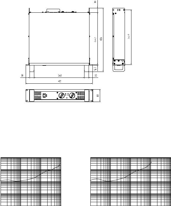
Dimensions (W × |
H × D) |
|
|
|
|
|
|
|
|
|
|
|
|
|
|
|
480 × 88 ×456 mm |
|
|
|
|
|
|
|
|||||||||||||||
|
|
|
|
|
|
|
|
|
|
|
|
|
|
|
|
|
|
|
|
|
|
|
|
|
|
|
|
|
|
|
|
|
|
|
|
|
|
||
Weight |
|
|
|
|
|
|
|
|
|
|
|
|
|
|
|
|
|
|
|
|
|
|
|
|
|
|
|
|
|
|
|
|
12 kg |
|
|
||||
|
|
|
|
|
|
|
|
|
|
|
|
|
|
|
|
|
|
|
|
|
|
|
|||||||||||||||||
Included Accessories |
|
|
|
|
|
|
|
|
|
Security cover (with a hex wrench), Owner s Manual |
|
|
|||||||||||||||||||||||||||
|
|
|
|
|
|
|
|
|
|
|
|
|
|
|
|
|
|
|
|
|
|
|
|
|
|
|
|
|
|
|
|
|
|
|
|
|
|
|
|
0 dBu=0.775 Vrms, Half Power=1/2 Power Output Level (Rated Power)
3

P5000S / P7000S
■
|
|
|
|
P5000S |
|
P7000S |
|
|
|
|
|
|
|
|
|
|
8 |
Ω/STEREO |
|
525 W ×2 |
|
750 W ×2 |
|
1 kHz |
4 |
Ω/STEREO |
|
750 W ×2 |
|
1100 W ×2 |
|
THD N = 1 % |
8 |
Ω/BRIDGE |
|
1500 W ×1 |
|
2200 W ×1 |
|
|
8 |
Ω/STEREO |
|
500 W ×2 |
|
700 W ×2 |
|
|
|
|
|
||||
20 Hz 20 kHz |
4 |
Ω/STEREO |
|
700 W ×2 |
|
950 W ×2 |
|
THD N = 0.1 % |
8 |
Ω/BRIDGE |
|
1400 W ×1 |
|
1900 W ×1 |
|
1 kHz |
|
|
|
|
|
|
|
2 |
Ω/STEREO |
|
1300 W ×2 |
|
1600 W ×2 |
|
|
20 ms nonclip |
4 |
Ω/BRIDGE |
|
2600 W ×1 |
|
3200 W ×1 |
|
|
|
|
|
|
|
||
|
Half Power |
10 Hz 40 kHz THD N = 0.5 % |
|
|
|||
THD N |
4 |
Ω 8 Ω/STEREO |
0.1 % |
|
|
||
20 Hz 20 kHz Half Power |
8 |
Ω/BRIDGE |
|
|
|||
|
|
|
|
|
|||
|
|
|
|
|
|||
|
RL = 8 Ω Po = 1 W |
0 dB +0.5 dB 1 dB f = 20 Hz 50 kHz |
|
|
|||
|
4 |
Ω 8 Ω/STEREO |
0.1 % |
|
|
||
60 Hz 7 kHz 4 1 Half Power |
8 |
Ω/BRIDGE |
|
|
|||
|
|
|
|
|
|||
|
Half Power RL = 8 Ω 1 kHz |
70 dB |
|
|
|||
. max. |
600 Ω |
|
|
||||
|
|
|
|
|
|||
min. |
20 Hz 20 kHz (DIN AUDIO) |
|
70 dBu |
|
|
||
SN |
20 Hz 20 kHz (DIN AUDIO) |
|
103 dB |
|
104dB |
|
|
|
|
|
|
|
|
||
|
RL = 8 Ω 1 kHz |
350 |
|
|
|||
max. Rated Power 8 Ω |
|
+6 dBu |
|
+8 dBu |
|
||
|
|
|
|
|
|
||
max. |
|
32.1 dB |
|
|
|||
|
|
|
|
|
|
||
|
|
|
30 kΩ/ 15 kΩ/ |
|
|
||
|
|
POWER ON/OFF |
|
|
|||
|
|
|
31 ×2 |
|
|||
|
|
|
|
|
|||
|
|
MODE STEREO/PARALLEL/BRIDGE |
|
|
|||
|
|
|
|
|
|||
|
|
|
SUB WOOFER/LOW CUT/OFF)×2 |
|
|||
|
|
|
fc = (25 Hz 150 Hz) ×2 |
|
|
||
|
|
|
YS Processing (ON/OFF) |
|
|
||
|
|
|
|
|
|||
|
INPUT |
XLR-3-31 |
|
|
|||
|
|
|
1/4 TRS |
|
|||
|
OUTPUT |
|
|
|
|||
|
|
|
5 |
|
|
||
|
|
|
1/4 |
|
|
||
|
POWER |
× 1 |
|
|
|||
|
PROTECTION |
×1 |
|
|
|||
|
TEMP |
×1 85 |
|
|
|||
|
CLIP |
×2 |
|
|
|||
|
SIGNAL |
×2 |
|
|
|||
|
YS Processing |
×1 |
|
|
|||
|
|
|
|
|
|
||
|
|
|
POWER / |
|
|
||
|
|
|
|
|
|
|
|
|
|
DC |
|
|
|||
|
|
|
|
|
|||
|
|
|
|
|
|||
|
|
|
90 VI RL 1 Ω |
|
|||
|
|
|
THD 0.5 |
|
|
||
|
|
|
|
|
|
||
|
|
|
100 V 50/60 Hz |
|
|
||
|
|
|
35 W |
|
35 W |
|
|
|
1/8 4 Ω |
|
550 W |
|
700 W |
|
|
|
4 Ω |
|
3000 W |
|
4000 W |
|
|
|
|
|
|
|
|
|
|
W × H × D |
|
|
480 × 88 × 456 mm |
|
|
||
|
|
|
|
12 kg |
|
|
|
|
|
|
6 |
|
|||
0 dBu = 0.775 Vrms Half Power = 1/2 Power Output Level (Rated Power)
4
P5000S /P7000S
■ DIMENSIONS
Unit: mm
■ PERFOMANCE GRAPHS
P5000S |
P7000S |
Power Consumption [W]
Mode:STEREO |
Mode:STEREO |
Both ch Driven |
Both ch Driven |
RL=4 Ω , f=1 kHz |
RL=4 Ω , f=1 kHz |
10000 |
10000 |
1000 |
|
|
|
|
[W] |
1000 |
|
|
|
|
|
100 |
|
|
|
|
Consumption |
100 |
|
|
|
|
|
|
|
|
|
|
|
|
|
|
|
||
10 |
|
|
|
|
Power |
10 |
|
|
|
|
|
|
|
|
|
|
|
|
|
|
|
||
1 |
1 |
10 |
100 |
1000 |
|
1 |
1 |
10 |
100 |
1000 |
10000 |
|
|
Output Power [W] |
|
|
|
|
|
Output Power [W] |
|
|
|
5
P5000S / P7000S
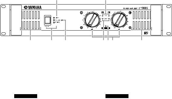
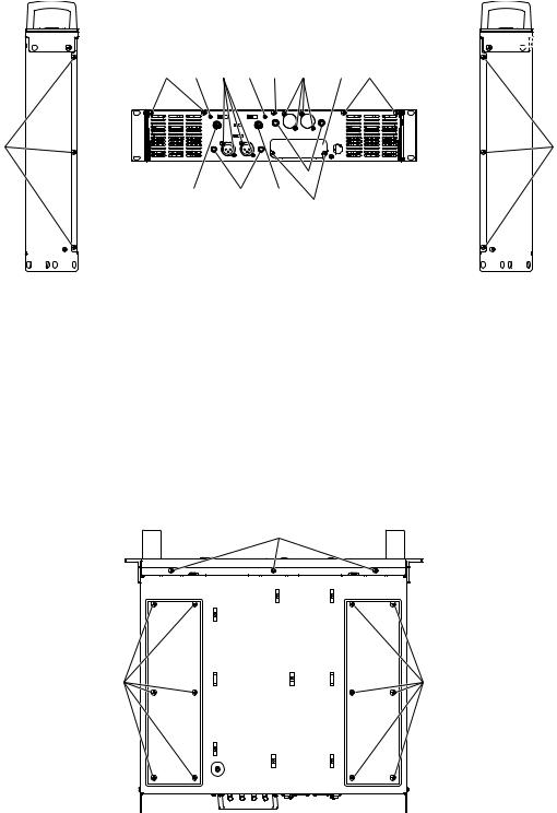
■ PANEL LAYOUT
Front Panel
w
i |
q |
e |
r |
tuy i
q [POWER] switch and indicator |
q [POWER] / |
||
w [TEMP] indicator |
w [TEMP] |
||
e [PROTECTION] indicator |
e [PROTECTION] |
||
r [CLIP] indicator |
r [CLIP] |
||
t [SIGNAL] indicator |
t [SIGNAL] |
||
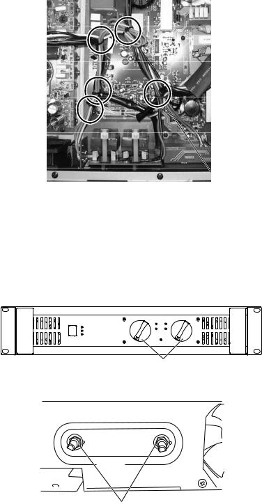
y Volume control knobs |
y |
|
|
u [ |
]indicator |
u [ |
] |
i Air intakes |
|
i |
|
6
P5000S /P7000S
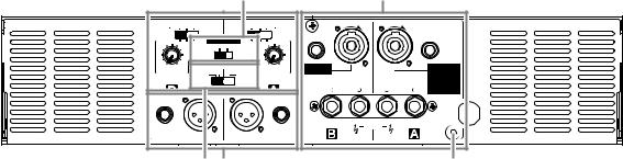
Rear Panel
|
|
|
qw |
|
|
|
|
|
|
t |
|
|
|
|
LOWCUT |
SUB |
|
SUB |
|
|
LOCK |
|
|
LOCK |
SPEAKERS |
||||
WOOFER OFF |
OFF WOOFER LOWCUT |
|
|
|
||||||||||
|
|
|
|
|
|
|
3 |
|
|
2 |
3 |
|
2 |
|
|
90 |
|
|
|
|
90 |
|
|
|
|
|
|
|
|
50 |
|
|
ON OFF |
|
50 |
|
|
|
|
|
|
|
|
|
|
|
125 |
|
|
|
125 |
|
|
|
|
|
|
|
|
25 |
Hz 150 |
STEREO BRIDGE |
PARALLEL |
25 |
Hz 150 |
+ 1 + |
|
|
|
|
|
1 + + |
||
FREQUENCY |
|
|
FREQUENCY |
- 1 - |
|
|
|
|
|
1 - |
- |
|||
|
|
|
|
|
|
|
|
2 + + |
||||||
|
|
|
|
|
|
|
|
|
|
|
|
|
2 - |
- |
|
|
|
INPUT |
|
|
|
- |
1 |
+ |
|
+ |
1 |
- |
|
|
|
|
|
|
|
|
|
|
|
|
|
|
|
|
|
|
|
|
|
|
|
|
|
(-) |
|
(+) |
|
|
|
|
|
|
|
|
|
|
|
|
|
BRIDGE |
|
|
|
|
|
|
|
re |
|
|
|
|
|
|
|
|
|
|
y |
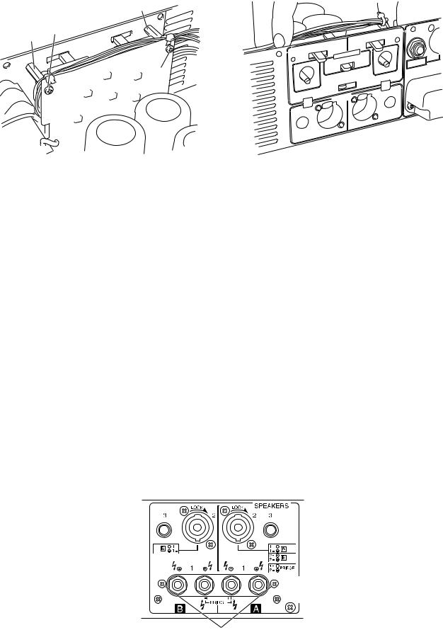
qFILTER switch and[FREQUENCY] adjustment knob (One pair for each channel)
w [ ] ON/OFF switch e [INPUT] jacks (Channels A, B)
r [STEREO/PARALLEL/BRIDGE] switch t [SPEAKERS] jacks
y GND terminal
q FILTER [FREQUENCY]
A B
w [ ] e [INPUT] A B
r [STEREO/PARALLEL/BRIDGE] t [SPEAKERS]
y GND
7

P5000S / P7000S
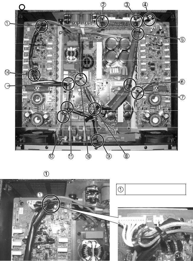
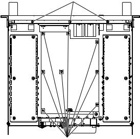
■ CIRCUIT BOARD LAYOUT&WIRING
PAH |
IN |
OUT1 |
OUT2 |
PS |
PAH |
VR
COIL |
LED |
PSW
OUT1 |
OUT2 |
IN

Rear Panel
The figure which looked at the front panel from the inner side
|
VR |
LED |
LED |
PSW |
|
FrontPanel |
|
8
P5000S /P7000S
Whole wiring drawing <Rev. 06>
See page 10 |
See page 10 See page 10 |
This point has a cord holder.

See page 9
See page 10
See page 11
 See page 10 See page 11
See page 10
|
See page 11,12 See page 11,12 See page 11 |
See page 10-12 See page 10-12 |
Detail drawing |
|
* The following "wiring ass’y" are tied. |
|
|
|
WA87380,WA87410 (VA19550),
WA87400
9
P5000S / P7000S
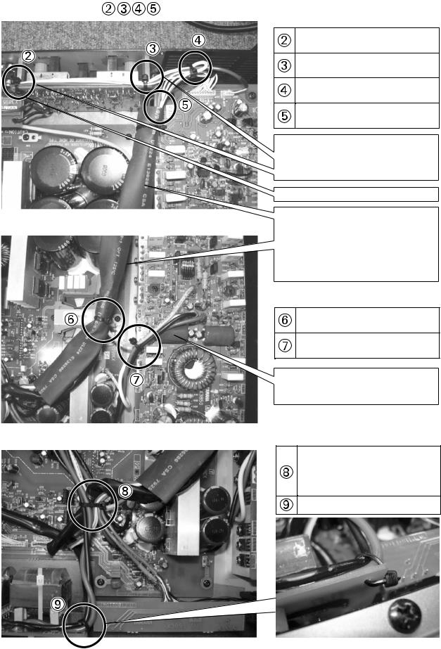
Detail drawing
Detail drawing 

Detail drawing 
* The following "wiring ass’y" are tied.
WA87410(VA19560,VA14660,
VA14730)
WA87410(VA19560,VA14660,
VA14730)
WA87410(VA19560,VA14660,
VA14730),WA87400
WA01090,WA87400,WA87410,
(VA14660,VA14730)
ATTENTION:
Tie the wires (WA87410) at the side of switch. WA87410
Soldering (WA01180)
ATTENTION:
WA87410 (VA14660,VA14730),and WA01090 are through the WB07260
(TUBE L=240mm)
WA87410,WA01090 WB07260 240mm
* The following "wiring ass’y" are tied.
WA01090,WA87370,WA87400, WA87410 (VA14660,VA14730)
WA87320,WA87330,WA87340,
WA87370
Need twist of two rotations.
2
(WA87320,WA87330,WA87340)
* The following "wiring ass’y" are tied.
WA01090,WA87400,WA87410
(VA14660,VA14730),WA87290, WA87310,WA87300*2,
COIL WIRING
COIL WIRING
10
P5000S /P7000S
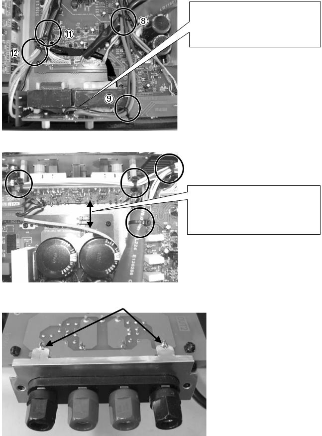
Detail drawing |
|
|
|
|
|
|
|
|
|
* The following "wiring ass'y" are tied. |
|||
|
|
|
|
|
||
|
|
|
|
|
WA87290,WA87300*2,WA87310, |
|
|
|
|
|
|
WA01110,WA01120,COIL WIRING |
|
|
|
|
|
|
WA87290,WA87300,WA87310, |
|
|
|
|
|
|
WA01110,WA01120,WA87400 |
|
|
|
|
|
|
WA87400,WA87380 |
|
|
|
|
|
|
|
|
|
|
|
|
|
|
|
|
|
|
|
ATTENTION: |
|
|
|
|
|
|
The COIL WIRING isn't at "U","A","K" |
|
|
|
|
|
|
destination. |
|
|
|
|
|
|
|
U,A,K |
|
|
|
|
|
|
|
|
|
|
|
|
Need twist of two rotations. |
||
|
|
2 |
||||
|
|
|
|
(WA87290,WA87300,WA87310) |
||
Detail drawing |
|
|
|
|
|
|
|
|
|
* The following "wiring ass'y" are tied. |
|||
|
|
|
|
|
|
|
|
|
|
|
|
|
|
|
|
|
|
|
WA01110,WA01120,WA87400, |
|
|
|
|
|
|
WA87420 |
|
|
|
|
|
|
WA01110,WA01120,FAN WIRING |
|
|
|
|
|
|
|
|
|
|
|
|
Need twist of three rotations. |
||
|
|
3 |
||||
|
|
|
|
(WA01110,WA01120) |
||
|
|
|
|
|
||
|
|
|
|
The wire of FAN has to be tense condition |
||
|
|
|
|
from the FAN to the tie of No.12 |
||
|
|
|
||||
|
|
|
!2 |
|||
Point of Notice H,B destination H,B |
||||||
|
|
|
|
|
|
|
|
|
|
|
The wires of following have to be tense |
|
|
|
|
|
|
condition. |
|
|
|
|
|
|
|||
|
|
|
|
1. From the FAN to the tie of No.12FAN. !2 |
||
|
|
|
|
2. From PSW to the tie of No.12PSW. !2 |
||
|
|
|
|
3. From CN412 to the tie of No.11CN412. !2 |
||
|
|
|
|
4. From CN411, CN408 to the tie of No.8. |
||
|
|
|
|
CN411,CN408 i |
||
|
|
|
|
5. From tie of No.9 to the tie of No.8. o i |
||
|
|
|
|
|
|
|
|
|
|
|
ATTENTION: |
||
|
|
|
|
Please wire a "WA87420" as a photograph. |
||
|
|
|
WA87420 |
|||
|
|
|
|
Need twist of three rotations. |
||
|
|
|
|
(Wire of coil) 3 |
||
11
P5000S / P7000S
Point of Notice J destination J
Setting of coil sheet is that there is the start of wire (W701,W702) at the side of top.
引き出します
Point of Notice
ATTENTION:
Please detach the wire of WA87370 from IN sheet.
WA87370 IN
Detail drawing OUT 2 |
Soldering EARTHFILM. |
|
|
||
OUT2 |
||
|
12
P5000S /P7000S
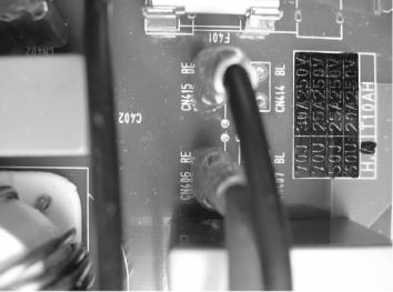
Connect of coils.
*Regarding to connect the wire of coil.
Please connect the Red wire to CN406.
Please connect the Black wire to CN415.
CN406,CN415
13
P5000S / P7000S
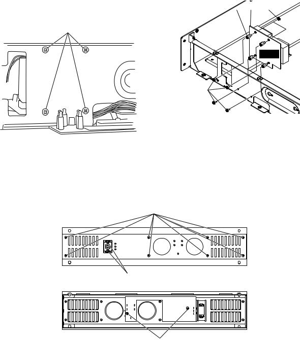
■ DISASSEMBLY PROCEDURE
1. |
Rack Angle (Time required: about 1 min.) |
1. : 1 |
|
1-1 |
Remove the three (3) screws marked [430] for each |
1-1 |
[430] 3 |
|
side. |
|
Fig.1 |
|
The rack angle can then be removed. (Fig.1) |
|
|
|
|
2. : 2 |
|
2. |
Top Cover (Time required: about 2 min.) |
2-1 |
[480] 11 |
2-1 |
Remove the eleven (11) screws marked [480]. |
|
Fig.1 |
|
The top cover can then be removed. (Fig.1) |
|
|
[430]
 [430]
[430]
[480] [280] [260] [280] [480] [320] |
[500] [480] |
[480] |
|
[480] |
|
|
[C] |
[230] |
[B] |
[230] |
|
|
[510] |
[230]: VR Knob (V9665200) VR (S)
[260]: Bonding Tapping Screw-B 3.0X8 MFZN2BL (VN413300) B [280]: Bind Head Tapping Screw-S 3.0X6 MFZN2BL (EP630210) + S
[320]: Flat Head Tapping Screw-B 3.0X8 MFZN2BL (EP600790) + B [430]: Bind Head Screw 4.0X12 MFZN2BL (VB132700) +
[480]: Bind Head Tapping Screw-B 4.0X8 MFZN2BL (EG340190) [510]: Bind Head Tapping Screw-S 3.0X6 MFZN2BL (EP630210) + S
|
(Fig.1) |
|
|
3. |
PA Unit (Time required: about 5 min.) |
3. |
PA : 5 |
3-1 |
Remove the rack angle. (See procedure 1.) |
3-1 |
1 |
3-2 |
Remove the top cover. (See procedure 2.) |
3-2 |
2 ) |
3-3 |
Remove the six screws marked [150] for each side |
3-3 |
[150] 6 |
|
from the bottom. |
|
PA Fig.2 |
|
The PA units can then be removed. (Fig.2) |
|
|
|
|
[410] |
|
[150] |
[150] |
[150]: Bind Head Tapping Screw-B 4.0X8 MFZN2BL (EG340190) + B [410]: Bind Head Tapping Screw-B 4.0X8 MFZN2BL (EG340190) + B
(Fig.2)
14
|
|
P5000S /P7000S |
4. PS Circuit Board (Time required: about 5 |
4. |
PS ( : 5 ) |
min.) |
4-1 |
(1 ) |
4-1 Remove the rack angle. (See procedure 1.) |
4-2 |
(2 ) |
4-2 |
Remove the top cover. (See procedure 2.) |
4-3 [180] 9 PS |
4-3 |
Remove the nine (9) screws marked [180]. |
Fig.3 |
|
The PS circuit board can then be removed. (Fig.3) |
|
|
|
[410] |
[180]
[180]: Bind Head Tapping Screw-S 3.0X6 MFZN2BL (EP630210) + S
[410]: Bind Head Tapping Screw-B 4.0X8 MFZN2BL (EG340190) + B
|
|
(Fig.3) |
|
5. IN Circuit Board (Time required: about 6 |
5. |
IN : 6 |
|
|
min.) |
5-1 |
1 |
5-1 Remove the rack angle. (See procedure 1.) |
5-2 |
2 |
|
5-2 Remove the top cover. (See procedure 2.) |
5-3 |
[260] 4 [280] 2 |
|
5-3 Remove the four (4) screws marked [260] and the |
|
Fig.1 |
|
|
two (2) screws marked [280]. (Fig.1) |
5-4 |
[B] 2 Fig.1 |
5-4 |
Remove the two (2) hexagonal nuts marked [B]. |
5-5 |
[280] 2 [270] |
|
(Fig.1) |
|
Fig.4 |
5-5 |
Remove the two (2) screws marked [280] to |
5-6 |
[230] 2 Fig.1 |
|
remove the two hex spacers marked [270]. (Fig.4) |
5-7 |
OUT2 W301 |
5-6 |
Remove the two (2) VR knobs marked [230].(Fig.1) |
|
IN W301A OUT2 |
5-7 |
Because the IN circuit board and the OUT2 circuit |
W301B IN |
|
|
board are connected by the connector assembly |
|
|
|
W301, it removes the solder of IN circuit board |
* |
IN |
|
terminal W301A or OUT2 circuit board terminal |
|
|
|
W301B. |
|
|
|
The IN circuit board can then be removed. |
|
Fig.5 |
*When reinstalling the IN circuit board, let the hooks of the XLM connectors out of the chassis at first, and inserts the jacks or switches into the holes on the chassis. (Fig.5)
15
P5000S / P7000S
[270]
[280]
[270]
[280]
[270]: Hex Spacer H=24.5 B=5.5 (WA058500)
[280]: Bind Head Tapping Screw-S 3.0X6 MFZN2BL (EP630210) + S
|
(Fig.4) |
|
(Fig.5) |
6. OUT1 Circuit Board (Time required: about 4 |
6. |
OUT1 : 4 |
|
|
min.) |
6-1 |
1 |
6-1 |
Remove the rack angle. (See procedure 1.) |
6-2 |
2 |
6-2 |
Remove the top cover. (See procedure 2.) |
6-3 [320] 4 Fig.1 |
|
6-3 |
Remove the four (4) screws marked [320]. (Fig.1) |
6-4 [C] 2 OUT1 |
|
6-4 |
Remove the two (2) hexagonal nuts marked [C]. |
|
Fig.1 |
|
The OUT1 circuit board can then be removed. |
* OUT1 OUT2 W607 |
|
|
(Fig.1) |
|
|
*The OUT1 circuit board and the OUT2 circuit
|
board are connected by the connector assembly W607. |
7. |
OUT2 : 5 |
7. OUT2 Circuit Board (Time required: about 5 |
7-1 |
1 |
|
7-2 |
2 |
||
|
min.) |
7-3 |
OUT1 6 |
7-1 Remove the rack angle. (See procedure 1.) |
7-4 [510] 2 [500] SP |
||
7-2 Remove the top cover. (See procedure 2.) |
|
Fig.1 |
|
7-3 |
Remove the OUT1 circuit board. (See procedure 6.) |
7-5 [310] 2 Fig.6 |
|
7-4 |
Remove the two (2) screws marked [510]. |
7-6 |
IN W301 |
|
Remove the SP terminal cover marked [500]. (Fig.1) |
|
W301B OUT2 |
7-5 |
Remove the two (2) screws marked [310]. (Fig.6) |
|
OUT1 |
7-6 |
Because the OUT2 circuit board and the IN circuit |
|
|
|
board are connected by the connector assembly |
|
|
|
W301, it removes the solder of terminal W301B. |
|
|
The OUT2 circuit board (and the OUT1 circuit board) can then be removed.
[310]
[310]: Bind Head Tapping Screw-B 3.0X12 MFZN2BL (VQ074600) + B
(Fig.6)
16
|
|
|
P5000S /P7000S |
8. Front Panel part (Time required: about 5 |
8. : |
||
|
min.) |
8-1 |
1 |
8-1 Remove the rack angle. (See procedure 1.) |
8-2 |
|
|
8-2 |
Remove the top cover. (See procedure 2.) |
8-3 5 |
|
8-3 |
Cuts Cord Holder (5 Point) of the Connector |
|
Fig.7 |
|
assembly. (Fig.7) |
8-4 |
[410] Fig.2,Fig.3 |
8-4 |
Remove the six (6) screws marked [410]. (Fig.2, |
8-5 |
|
|
Fig.3) |
|
|
8-5 |
Draws out in front of the front panel part. |
|
|
Front Panel side•ƒ !"#$%‘&
|
(Fig.7) |
|
|
9. |
VR Circuit Board (Time required: about 6 |
9. |
VR : 6 |
|
min.) |
9-1 |
8 |
9-1 |
Remove the front panel part. (See procedure 8.) |
9-2 |
[130] |
9-2 |
Remove the attenuator knobs marked [130]. (Fig.8) |
|
Fig.8 |
9-3 |
Remove the two (2) hexagonal nuts marked [A]. |
9-3 |
[A] 2 VR |
|
The VR circuit board can then be removed. (Fig.9) |
|
Fig.9 |
[130]
[130]: Attenuator Knob (WA059300)
(Fig.8)
[A]
(Fig.9)
17
P5000S / P7000S |
|
|
|
|
|
|
|
10. Coil circuit board (Time required: about 7 |
10. |
: 7 |
|||||
|
min.) |
10-1 8 |
|||||
10-1 Remove the front panel part. (See procedure 8.) |
10-2 |
PS 4 |
|||||
10-2 |
Remove the PS circuit board. (See procedure 4.) |
10-3 [60] 4 |
|||||
10-3 |
Remove the four (4) screws marked [60]. |
|
Fig.10 |
|
|
|
|
|
The coil circuit board can then be removed. |
10-4 [70] 4 [65] |
|||||
|
(Fig.10) |
|
4 Fig.11 |
||||
10-4 |
Remove the four (4) hexagonal nuts marked [70]. |
* |
|
||||
|
The four (4) spacers can then removed marked |
|
” ” CN406 ” ” CN415 |
||||
|
[65]. (Fig.11) |
|
|
|
|
|
|
|
|
|
|
|
|
|
|
* When reinstalling the COIL circuit board, connect |
|
|
[65] |
[50] |
[70] |
|
|
|
|
|
|
|
|
||
the Red wire to CN406 and the Black wire to CN415. [60]
COIL
[60]
[60]: Bind Head Tapping Screw-S 3.0X8 MFZN2BL (EP600530)
+ S
[60]: Bind Head Tapping Screw-S 3.0X8 MFZN2BL (EP600530)
+ S
[65]:Spacer H=7.5 B=5.5 (WA058400)
[70]:Hexagonal Nuts 4.0 MFZN2BL (03760280)
|
(Fig.10) |
|
(Fig.11) |
|
|
|
|
11. LED Circuit Board (Time required: about 5 |
11. |
LED : 5 |
|
|
min.) |
11-1 |
8 |
11-1 |
Remove the front panel part. (See procedure 8.) |
11-2 |
[120] 2 LED |
11-2 |
Remove the two (2) screws marked [120]. |
|
Fig.12 |
|
The LED circuit board can then be removed. |
[360] |
|
|
(Fig.12) |
|
|
[90]
[120]
[90]: Bind Head Tapping Screw-S 3.0X6 MFZN2BL (EP630210) + S [120]: Bind Head Tapping Screw-S 3.0X6 MFZN2BL (EP630210) + S [360]: Hex Socket Tapping Screw-S3.0X10 MFZN2BL (WA673200) S
(Fig.12)
18
|
|
|
|
|
|
|
|
|
|
|
P5000S /P7000S |
12. PSW Circuit Board (Time required: about |
12. |
PSW : 10 |
|||||||||
|
10 min.) |
12-1 8 |
|||||||||
12-1 |
Remove the front panel part. (See procedure 8.) |
12-2 [400] PSW |
|||||||||
12-2 |
Remove the power switch escutcheon marked |
|
Fig.13 |
||||||||
|
[400]. (Fig.13) |
12-3 [100] PSW |
|||||||||
12-3 |
It presses lightly from the panel back and remove |
|
|
||||||||
|
the power switch knob marked [100]. |
* |
L |
||||||||
|
|
|
PSW |
||||||||
|
* When it is hard to remove the power switch |
|
Fig.14 |
||||||||
|
knob, insert an L-shaped rod into the gap and pull |
|
|
||||||||
|
out the knob as shown the illustration. (Fig.14) |
|
|
||||||||
|
Be careful so as not to bruise a panel and a knob at |
12-4 [90] 2 PSW |
|||||||||
|
this time. |
|
Fig.12 |
||||||||
12-4 |
Remove the two (2) screws marked [90]. |
|
|
|
|
|
|
|
|
|
|
|
The PSW circuit board can then be removed. |
|
|
|
|
|
|
|
|
|
|
|
(Fig.12) |
|
|
|
|
|
|
|
|
|
|
|
[400] |
|
|
|
|
|
|
|
|
|
|
|
|
|
|
|
|
|
|
|
|
|
|
[100]
|
|
[100]: Power Switch Knob (WA059000) PSW |
|
|
(Fig.14) |
[400]: Power Switch Escutcheon (WA060700) |
|
|
PSW |
|
|
(Fig.13) |
|
|
13. Handle (Time required: about 6 min.) |
13. |
: 6 |
13-1 Remove the front panel part. (See procedure 8.) |
13-1 |
8 |
13-2 Remove the two (2) screws marked [390] for each |
13-2 |
[390] 2 |
side. |
|
Fig.15 |
The handles can then be removed. (Fig.15) |
|
|
|
* |
|
*The handle angle is removed simultaneously, at this time.
Handle Angle
[390]
[390]: Bind Head Screw SP 5.0X10 MFZN2BL (VU688100) +
(Fig.15)
Handle Angle
19
P5000S / P7000S
14.Disassemble of Front Panel 1 and Front 14. 1
|
Panel 2 (Time required: about 8 min.) |
|
2 : 8 |
14-1 Remove the front panel part. (See procedure 8.) |
14-1 |
8 |
|
14-2 Remove the handles. (See procedure 13.) |
14-2 |
13 |
|
14-3 Remove the eight (8) hex socket tapping screws |
14-3 |
[360] S 8 |
|
|
marked [360]. |
|
1 2 |
|
The front panel 1 and the front panel 2 can then be |
|
(Fig.12) |
|
disassembled. (Fig.12) |
|
|
|
|
15. |
DC : 12 |
|
|
15-1 8 |
|
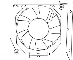
15. Fan (Time required: about 12 min.) |
15-2 |
DC PA |
|
15-1 |
Remove the front panel part. (See procedure 8.) |
|
3 |
15-2 |
Remove the PA unit located on the same side as the |
15-3 |
[30] 2 DC |
|
fan to remove. (See procedure 3.) |
|
(Fig.16) |
15-3 |
Remove the two (2) screws marked [30] for each |
|
|
side.
Fans can then be removed. (Fig.16)
[30]
[30]
[30]: Bind Head Screw SP 4.0X16 MFZN2Y (VB764900) +
(Fig.16)
20
P5000S /P7000S
■ IC BLOCK DIAGRAMIC
• NJM2068MD-T1 (XJ553A00) Dual Operational Amplifier
P5000S IN: IC301, IC302, IC303, IC304, IC305, IC306, IC307
PAH: IC201
P7000S IN: IC301, IC302, IC303, IC304, IC305, IC306, IC307
PAH: IC201
Output A |
1 |
|
|
|
|
|
Inverting |
2 |
|
|
|
|
|
Input A |
|
|
- |
|
+ |
|
Non-Inverting |
3 |
|
|
|
|
|
|
|
|
|
|
||
Input A |
|
|
|
|
|
|
|
|
|
|
|
|
|
-DC Voltage Supply |
4 |
-V |
|
|
||
|
+V 8 |
+DC Voltage |
|
|
Supply |
||
|
|
||
|
7 |
Output B |
|
+ - |
6 |
Inverting |
|
Input B |
|||
|
5Non-Inverting Input B
 IR2110 (X2382A00) DRIVER
P5000S PS: IC402
P7000S PS: IC402
LO |
1 |
14 |
|
COM |
2 |
13 |
VSS |
VCC |
3 |
12 |
LIN |
|
4 |
11 |
SD |
VS |
5 |
10 |
HIN |
VB |
6 |
9 |
VDD |
HO |
7 |
8 |
|
|
|
|
|
|
|
|
6 |
VB |
|
|
|
|
|
UV |
|
|
|
VDD |
9 |
|
|
HV |
DETECT |
R |
Q |
|
|
|
|
|
|
|
|||
|
|
|
|
LEVEL |
PULSE |
R |
7 |
HO |
|
RS Q |
|
SHIFT |
|||||
|
|
|
||||||
|
VDD/VCC |
FILTER |
S |
|
|
|||
HIN |
10 |
|
LEVEL |
|
|
|
|
|
|
|
|
SHIFT |
PULSE |
|
|
5 |
VS |
|
|
|
|
|
|
|||
|
|
|
|
GEN |
|
|
|
|
SD |
11 |
|
|
|
|
|
3 |
VCC |
|
|
|
|
|
UV |
|
|
|
|
|
|
VDD/VCC |
|
DETECT |
|
|
|
|
|
|
|
|
|
|
|
|
LIN |
12 |
|
LEVEL |
|
|
|
1 |
LO |
|
|
S |
SHIFT |
|
|
|
|
|
|
R |
Q |
|
|
DELAY |
|
|
|
VSS |
13 |
|
|
|
|
|
2 |
COM |
|
|
|
|
|
|
|
||
SG3525AN (X2383A00) |
|
|
|
|
|
|
|
||||
Regulating Pulse Width Modulator |
|
|
|
|
|
|
|||||
P5000S PS: IC401 |
|
|
|
|
|
|
|
|
|||
P7000S PS: IC401 |
|
VREF |
16 |
|
REFERENCE |
|
15 |
+VIN |
|||
|
|
|
|
|
REGULATOR |
|
|||||
|
|
|
|
OSC. OUTPUT |
4 |
|
FLIP/ |
|
|
|
|
INV. INPUTN |
1 |
16 |
VREF |
|
FLOP |
|
|
|
|||
|
|
|
|
13 |
VC |
||||||
|
|
|
|
|
|||||||
|
|
|
|
|
|
|
|
|
|||
N.I. INPUT |
2 |
15 |
+VIN |
SYNC |
3 |
OSCILLATOR |
|
|
|
|
|
|
|
|
|
|
|
||||||
SYNC |
3 |
14 |
OUTPUT B |
RT |
6 |
A |
11 |
OUTPUT A |
|||
|
|||||||||||
|
|
|
|
|
|
|
|||||
|
|
|
|
DISCHARGE |
7 |
|
|
|
|
|
|
OSC. OUTPUT |
4 |
13 |
VC |
CT |
|
|
|
|
|
|
|
|
|
|
|
5 |
|
B |
14 |
OUTPUT B |
|||
|
|
|
|
|
|
|
|||||
CT |
5 |
12 |
GROUND |
|
|
|
|
|
|
|
|
RT |
6 |
11 |
OUTPUT A |
COMPENSATION |
9 |
|
PWM |
|
12 |
GROUND |
|
|
|
|
|
||||||||
|
|
|
|
|
|
|
50 |
A |
8 |
SOFT-START |
|
|
|
|
|
|
|
|
|
|
|||
DISCHARGE |
7 |
10 |
SHUTDOWN |
INV. INPUTN |
1 |
|
5K |
|
5K |
|
|
|
|
|
|
E/A |
|
|
|
||||
|
|
|
|
|
|
|
|
10 |
SHUTDOWN |
||
SOFT-START |
8 |
9 |
COMPENSATION |
N.I. INPUT |
2 |
|
|
|
|||
|
|
|
|
|
|||||||
|
|
|
|
|
|
|
|||||
21
P5000S / P7000S |
|
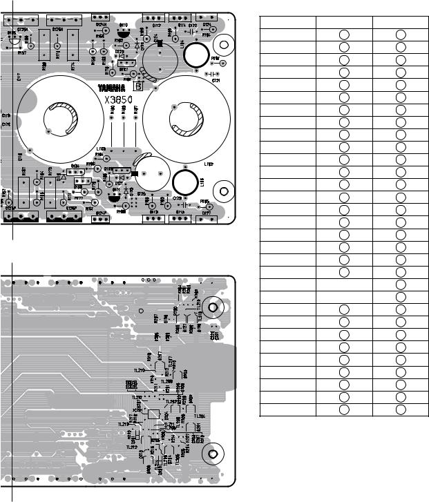
■ CIRCUIT BOARDS |
|
CONTENTS |
|
● PAH Circuit Board (X3850B0) ....................................................................................... |
23 |
● PS Circuit Board (X3851B0) ......................................................................................... |
25 |
● IN Circuit Board (X3501C0) .......................................................................................... |
29 |
● LED Circuit Board (X3895B0) ....................................................................................... |
30 |
● OUT1 Circuit Board (X3895B0) .................................................................................... |
31 |
● OUT2 Circuit Board (X3895B0) .................................................................................... |
32 |
● PSW Circuit Board (X3895B0) ...................................................................................... |
33 |
● VR Circuit Board (X3895B0) ......................................................................................... |
33 |
● COIL Circuit Board (X4945A0) ...................................................................................... |
34 |
22
|
|
P5000S /P7000S |
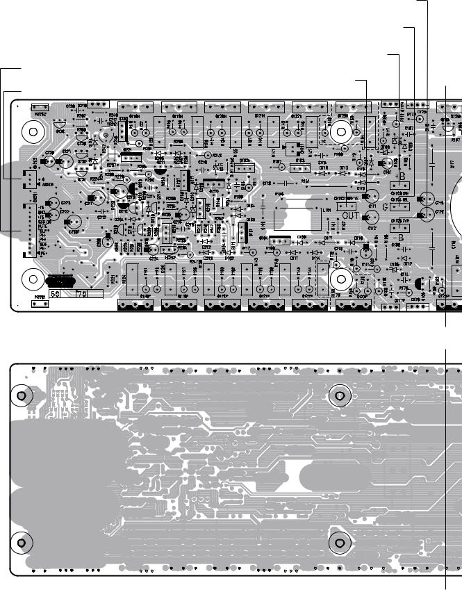
● PAH Circuit Board |
to PS-(W408(Bch)W403(Ach) |
|
|
||
|
to PS-(W407(Bch)W402(Ach) |
|
CN412(Ach) |
to PS-(W401(Ach) |
|
W406(Bch) |
|
|
to PS-(CN411(Bch) |
W604(Ach) |
|
to IN-CN301(Ach,Bch) |
to OUT2-(W606(Bch) |
A |
|
|
|
|
|
A’ |
|
|
B |
B’ |
23
P5000S / P7000S
A |
|
Following semi-conductors are installed for the PA unit. |
||
PA |
||||
|
||||
|
|
ref. |
P5000S P7000S |
|
|
|
D124 |
|
|
|
|
D125 |
|
|
|
|
D126 |
|
|
|
|
D127 |
|
|
|
|
Q112 |
|
|
|
|
Q113 |
|
|
|
|
Q114 |
|
|
|
|
Q115 |
|
|
|
|
Q117N |
|
|
|
|
Q117P |
|
|
|
|
Q118N |
|
|
|
|
Q118P |
|
|
|
|
Q119N |
|
|
|
|
Q119P |
|
|
|
|
Q120N |
|
|
|
|
Q120P |
|
|
|
Component side |
Q121N |
|
|
A’ |
|
Q121P |
|
|
B |
|
Q122N |
|
|
|
|
Q122P |
|
|
|
|
Q123N |
|
|
|
|
Q123P |
|
|
|
|
Q124N |
|
|
|
|
Q124P |
|
|
|
|
Q125N |
|
|
|
|
Q125P |
|
|
|
|
Q126N |
|
|
|
|
Q126P |
|
|
|
|
Q218 |
|
|
|
|
PR201 |
|
|
|
|
PR202 |
|
|
|
|
○ :Installed :not installed |
||
B’ |
Pattern side |
|
|
|
|
|
2NAP-WB10830 (P5000S) |
||
|
|
|
||
|
|
|
2NAP-WB10820 (P7000S) |
|
24

● PS Circuit Board
to FAN(Ach)
to PAH-CN201(Ach)
to PAH-CN201(Bch)
to IN-CN301
to FAN(Bch)
|
|
P5000S /P7000S |
|
|
to PSW-W602 (or W601) |
|
|
to LED-CN601 |
TEMP LED TEST POINT |
A |
|
|
|
||
to PAH-CN103(Bch) |
to PAH-CN105(Bch) |
|
|
to PAH-CN104(Bch) |
to PAH-CN105(Ach) |
|
A’ |
|
|
|
|
FAN TEST POINT |
|
|
|
to PAH-CN104(Ach) |
|
|
|
||
|
to PAH-CN103(Ach) |
|||
|
|
|||
25
Loading...