


PC-3301-N
Table of contents
 Loading...
POWER AMPLIFIER
PC6501N
/
PC4801N
/
PC3301N
/
PC2001N
SERVICE MANUAL
PC6501N
このサービ スマニ ュア ルはエ コパルプ
(ECF : 無塩素系漂白パルプ) を使用 し ていま す。
This document is printed on chlorine free (ECF) paper.
011763
PA
PC6501N: 200412-399000
PC4801N: 200412-367500
PC3301N: 200412-315000
PC2001N: 200412-283500
■ CONTENTS(目次)
SPECIFICATIONS(総合仕様).........................................................3/4
PANEL LAYOUT
CIRCUIT BOARD LAYOUT
DIMENSIONS
PERFORMANCE GRAPHS
DISASSEMBLY PROCEDURE
NOTES ON WIRING
LSI PIN DESCRIPTION
IC BLOCK DIAGRAM
CIRCUIT BOARDS
INSPECTIONS
PARTS LIST
BLOCK DIAGRAM
WIRING DIAGRAM(基板結線図)
OVERALL CIRCUIT DIAGRAM(総回路図)
Copyright (c) Yamaha Corporation. All rights reserved. PDF-K9051 ’05.01
(パネルレイアウト)..................................................5
(ユニットレイアウト)..............................6
(寸法図)......................................................................7
(特性図).................................................8
(分解手順)........................................9
(配線上の注意)...........................................14/15
(LSI端子機能表)........................................16
(ICブロック図)..............................................17
(シート基板図)...................................................19
(検査).................................................................30/38
(ブロックダイアグラム)
HAMAMATSU, JAPAN
PC6501N/PC4801N/PC3301N/PC2001N
IMPORTANT NOTICE
This manual has been provided for the use of authorized Yamaha Retailers and their service personnel. It has been assumed that basic
service procedures inherent to the industry, and more specifically Yamaha Products, are already known and understood by the users, and
have therefore not been restated.
WARNING : Failure to follow appropriate service and safety procedures when servicing this product may result in personal injury,
destruction of expensive components and failure of the product to perform as specified. For these reasons, we advise
all Yamaha product owners that all service required should be performed by an authorized Yamaha Retailer or the
appointed service representative.
IMPORTANT : This presentation or sale of this manual to any individual or firm does not constitute authorization certification,
recognition of any applicable technical capabilities, or establish a principal-agent relationship of any form.
The data provided is belived to be accurate and applicable to the unit(s) indicated on the cover. The research engineering, and service
departments of Yamaha are continually striving to improve Yamaha products. Modifications are, therefore, inevitable and changes in
specification are subject to change without notice or obligation to retrofit. Should any discrepancy appear to exist, please contact the
distributor’s Service Division.
WARNING : Static discharges can destroy expensive components. Discharge any static electricity your body may have
accumulated by grounding yourself to the ground bus in the unit (heavy gauge black wires connect to this bus).
IMPORTANT : Turn the unit OFF during disassembly and parts replacement. Recheck all work before you apply power to the unit.
WARNING: CHEMICAL CONTENT NOTICE!
The solder used in the production of this product contains LEAD. In addition, other electrical/electronic and/or plastic (Where applicable)
components may also contain traces of chemicals found by the California Health and Welfare Agency (and possibly other entities) to
cause cancer and/or birth defects or other reproductive harm.
DO NOT PLACE SOLDER, ELECTRICAL/ELECTRONIC OR PLASTIC COMPONENTS IN YOUR MOUTH FOR ANY REASON WHAT
SO EVER!
Avoid prolonged, unprotected contact between solder and your skin! When soldering, do not inhale solder fumes or expose eyes to
solder/flux vapor!
If you come in contact with solder or components located inside the enclosure of this product, wash your hands before handling food.
WARNING: THIS APPARATUS MUST BE EARTHED
■ WARNING
IMPORTANT
THE WIRES IN THIS MAINS LEAD ARE COLOURED IN
ACCORDANCE WITH THE FOLLOWING CODE:
GREEN-AND-YELLOW : EARTH
BLUE : NEUTRAL
BROWN : LIVE
As the colours of the wires in the mains lead of this apparatus
may not correspond with the coloured markings identifying the
terminals in your plug, proceed as follows:
The wire which is coloured GREEN and YELLOW must be
connected to the terminal in the plug which is marked by the
letter E or by the safety earth symbol or coloured GREEN
and YELLOW. The wire which is coloured BLUE must be
connected to the terminal which is marked with the letter N or
coloured BLACK.
The wire which is coloured BROWN must be connected to the
terminal which is marked with the letter L or coloured RED.
Components having special characteristics are marked
and must be replaced with parts having specification equal to
those originally installed.
印の商品は、 安全を維持す る た めに重要な部品です。 交
換する 場合は、安全のために必ず指定の部品 を ご使用 く ださ い。
* This applies only to products distributed by YAMAHA KEMBLE
MUSIC (U.K.) LTD.
2
■ SPECIFICATIONS
PC6501N/PC4801N/PC3301N/PC2001N
Power output level (Rated power)
1 kHz, THD+N=1 % 8 Ω/STEREO 700 W x 2 750 W x 2 550 W x 2 500 W x 2 350 W x 2 400 W x 2 230 W x 2 250 W x 2
20 Hz-20 kHz, THD+N=0.1 % 8 Ω/STEREO 650 W x 2 650 W x 2 475 W x 2 450 W x 2 330 W x 2 350 W x 2 200 W x 2 230 W x 2
1 kHz, 20 mS nonclip 2 Ω/STEREO 1500 W x 2 1600 W x 2 1200 W x 2 1200 W x 2 800 W x 2 900 W x 2 500 W x 2 600 W x 2
Power bandwidth
Half power
Total harmonic distortion (THD+N)
20 Hz-20 kHz, Half power
Frequency response MAX 0 dB
RL=8 Ω, Po=1 W, TYP 0 dB
f=20 Hz-50 kHz MIN –1 dB
Intermodulation distortion (IMD)
60 Hz:7 kHz, 4:1, Half power
Channel separation
Vol. max., Input 600 Ω shunt
Residual noise
Vol. min., 20 Hz-20 kHz (DIN AUDIO)
SN ratio
20 Hz-20 kHz (DIN AUDIO)
Damping factor
RL=8 Ω, f=1 kHz
Sensitivity
Vol. max., Rated power into 8 Ω
Voltage gain
Vol. max.
Maximam input voltage MIN +22 dBu
Input impedance TYP 20 kΩ/Balanced, 10 kΩ/Unbalanced
Controls Front panel POWER switch (ON/OFF)
Connectors Input XLR-3-31 type /ch
Indicators POWER/STAND-BY Green/Orange
Level meters 10 points LED meter /ch
Load protection POWER switch ON muting, DC detection
Amp. protection Temp. detection (heatsink temp≥90°C), VI limiter (RL≤1 Ω)
Limiter Comp.: THD≥0.5 %
Cooling Dual variable-speed fan
Power requirements U, V, T 120 V, 60 Hz
Power consumption Idling 40 W
Dimensions (W x H x D) 480 x 88 x 456 mm
Weight 12.5 kg
Accessories Power cord, Security cover, Owner’s manual, 3-pin Euroblock connector x 2
4 Ω/STEREO 1100 W x 2 1150 W x 2 850 W x 2 800 W x 2 600 W x 2 700 W x 2 400 W x 2 450 W x 2
8 Ω/BRIDGE 2200 W 2300 W 1700 W 1600 W 1200 W 1400 W 800 W 900 W
4 Ω/STEREO 930 W x 2 930 W x 2 725 W x 2 700 W x 2 525 W x 2 550 W x 2 325 W x 2 400 W x 2
8 Ω/BRIDGE 1860 W 1860 W 1450 W 1400 W 1050 W 1100 W 650 W 800 W
16 Ω/BRIDGE (100 V) - - - - 625 W 625 W - -
4 Ω/BRIDGE 3000 W 3200 W 2400 W 2400 W 1600 W 1800 W 1000 W 1200 W
TYP 32 dB
Rear panel MODE switch (STEREO/BRIDGE/PARALLEL)
Output SPEKON /ch, 5-way binding posts
Network RJ45 x 2
Power AC inlet
PROTECTION Red
TEMP Red (heatsink temp≥85°C)
REMOTE Green
H, B, W, K, O 230 V, 50/60 Hz
A 240 V, 50/60 Hz
Output power, 4 Ω
PC6501N PC4801N PC3301N PC2001N
120 V (U, V, T)/
240 V (A)
10 Hz-40 kHz (THD+N=0.5 %)
≤0.1 %
≤0.1 %
≥70 dBHalf power, RL=8 Ω, 1 kHz,
≤-70 dBu
105 dB 103 dB 101 dB 100 dB
≥800 ≥500
+8 dBu +6 dBu +4.5 dBu +3 dBu
Volume (31 positions) /ch
HPF switch (ON/OFF) /ch fc=20 Hz 12 dB/octave
DIP switch (6P)
Euroblock connector (balance) /ch
700 W (U, V, T)/
800 W (A)
230 V
(H, B, W, K, O)
800 W
(H, B, W, K, O)
120 V (U, V, T)/
240 V (A)
450 W (U, V, T)/
600 W (A)
230 V
(H, B, W, K, O)
600 W
(H, B, W, K, O)
120 V (U, V, T)/
240 V (A)
450 W (U, V, T)/
500 W (A)
230 V
(H, B, W, K, O)
500 W
(H, B, W, K, O)
120 V (U, V, T)/
240 V (A)
350 W
230 V
(H, B, W, K, O)
0 dBu=0.775 Vrms, Half power=1/2 Output power (3 dB below rated power)
3
PC6501N/PC4801N/PC3301N/PC2001N
■ 総合仕様
PC6501N PC4801N PC3301N PC2001N
出力レ ベル
1kHz、 THD + N = 1% 8Ω/STEREO 750W × 2 500W × 2 350W × 2 230W × 2
20Hz ~ 20kHz、 THD + N = 0.1%
1kHz, 20mS nonclip 2Ω/STEREO 1500W × 2 1100W × 2 800W × 2 500W × 2
出力帯域幅
Half power
全高調波帯域 (THD + N)
20Hz ~ 20kHz、 Half power
周波数特性 MAX 0dB
RL=8Ω、Po=1W、 TYP 0dB
f = 20Hz ~ 50kHz MIN - 1dB
混変調歪率 (IMD)
60Hz : 7kHz、 4 : 1、 Half power
チャンネルセパレーシ ョ ン
ボ リ ューム最大、 入力 600Ω シ ャ ン ト
残留 ノ イズ
ボ リ ューム最小、 20Hz ~ 20kHz (DIN AUDIO)
SN 比
20Hz ~ 20kHz (DIN AUDIO)
ダンピングフ ァ ク ター
RL = 8Ω、 f = 1kHz
入力感度
ボ リ ューム最大、 Rated power : 8Ω
ボルテージゲイ ン
ボリューム最大
最大許容入力電圧 MIN + 22dBu
入力イ ン ピーダン ス TYP 20kΩ/ バラ ンス型、 10kΩ/ ア ンバ ラ ンス型
コ ン ト ロール フ ロ ン ト パネル POWER スイ ッチ (ON/OFF)
コ ネ ク タ ー 入力 XLR-3-31 タ イ プ
インジケーター POWER/STAND-BY 緑 / オレンジ
レベルメーター 10 ポイ ン ト LED メーター
ロード プロテクシ ョ ン POWER スイ ッチオン ミ ュー ト、 DC 検出
アン プ プ ロ テ ク シ ョ ン 温度検出 (ヒ ー ト シン ク温度≧ 90 ℃)、 VI リ ミ ッ ター (RL ≦ 1Ω)
リミッター コンプ:THD≧0.5%
クー リ ング 連続可変式フ ァ ン
電源 100V、 50/60Hz
消費電力 無信号 40W
最大外形寸法 (W × H × D) 480 × 88 × 456mm
重量 12.5kg
付属品
0 dBu=0.775 Vrms, Half power=1/2 Output power (3 dB below rated power)
4Ω/STEREO 1100W × 2 800W × 2 600W × 2 350W × 2
8Ω/BRIDGE 2200W 1600W 1200W 700W
8Ω/STEREO 650W × 2 450W × 2 315W × 2 200W × 2
4Ω/STEREO 930W × 2 650W × 2 500W × 2 325W × 2
8Ω/BRIDGE 1860W 1300W 1000W 650W
16Ω/BRIDG (100V) - - 625W -
4Ω/BRIDGE 3000W 2200W 1600W 1000W
10Hz ~ 40kHz (THD + N = 0.5%)
≦0.1%
≦0.1%
≧70dBHalf power、 RL = 8Ω、 1kHz、
≦- 70dBu
105dB 103dB 101dB 100dB
≧800 ≧500
+8dBu +6dBu +4.5dBu +3dBu
TYP 32dB
ボ リ ューム (31 ポジシ ョ ン)
リ アパネル MODE ス イ ッ チ (STEREO/BRIDGE/PARALLEL)
HPF スイ ッチ (ON/OFF) fc = 20Hz 12dB/octave
DIP ス イ ッ チ (6P)
ユーロ ブロ ッ ク コ ネ ク タ ー (バランス)
出力 スピ コ ン、 5 ウ ェ イ ・ バイ ンデ ィ ング ・ ポス ト
ネッ トワーク RJ45 × 2
電源 AC イ ンレ ッ ト (PC6501N を除 く )
PROTECTION 赤
TEMP 赤 ( ヒ ー ト シ ン ク温度≧ 85 ℃)
REMOTE 緑
規定出力、 4Ω 800W 600W 450W 300W
電源コー ド (PC6501N を除 く )、 セキュ リテ ィ カバー、 取扱説明書、 3 ピンユーロ ブ ロ ッ ク コ ネ ク ター x 2
4
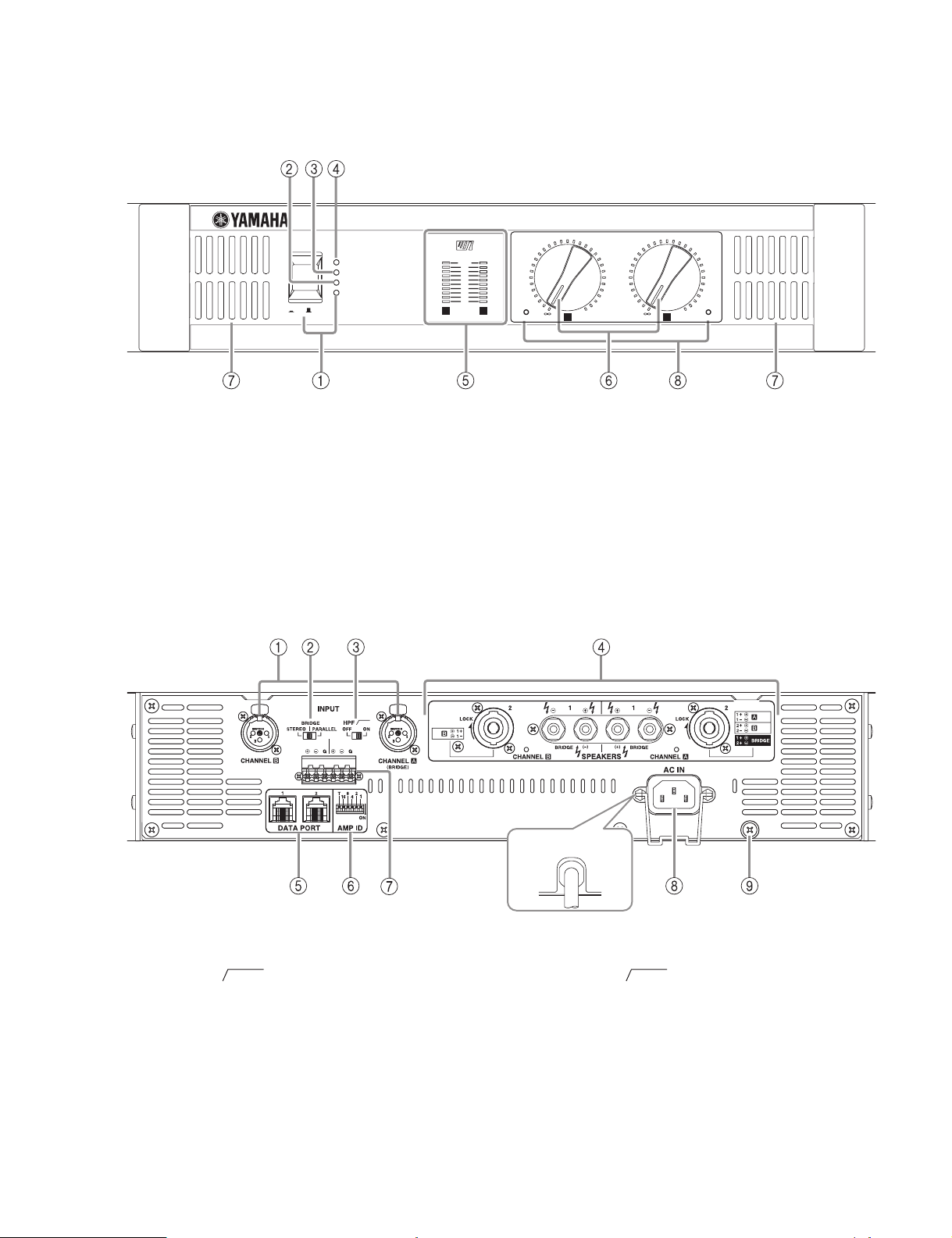
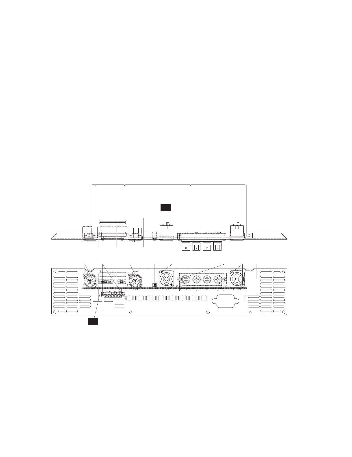
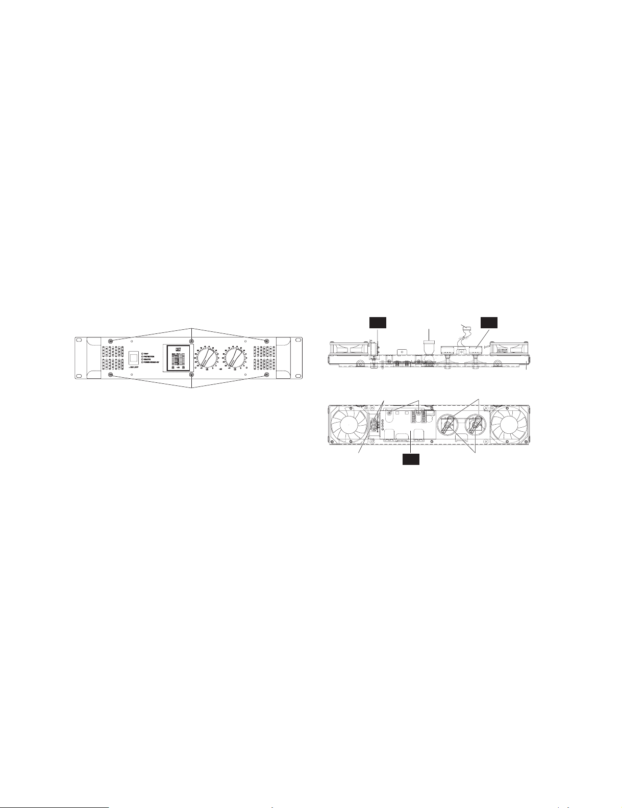
■ PANEL LAYOUT(パネルレイアウト)
• Front Panel(フロントパネル)
PC6501N/PC4801N/PC3301N/PC2001N
OFFON/
1 POWER/STAND-BY switch and indicator
2 REMOTE indicator
3 PROTECTION indicator
4 TEMP indicator
5 Level meters
6 Volume knobs
7 Air intakes
8 Security cover
• Rear Panel(リアパネル)
TEMP
PROTECTION
REMOTE
POWER/STAND-BY
EEEngine
CLIP
8
6
9
12
15
18
21
24
27
-dB
A B
16
18
20
25
30
35
50
A B
14
12
10
0
18
20
8
25
6
30
4
35
2
50
-dB
16
POWER AMPLIFIER
14
12
10
0
2
1 POWER/STAND-BY
PC 6501N
8
6
4
スイッチ、インジケーター
2 REMOTE インジケーター
3 PROTECTION インジケーター
4 TEMP インジケーター
5 レベルメーター
6
ボリュームツマミ
7 吸気口
8 セキュリティカバー
20Hz
1 XLR inputs
2 MODE switch
3 HPF switches
20 Hz 20 Hz
4 SPEAKERS jacks
5 DATA PORT jacks
6 AMP ID switch
7 Euroblock connector
8 AC inlet (except PC6501N (J))
9 GND terminals
In case of PC6501N (J)
(
PC6501N (J)
の場合)
1 XLR
2 MODEスイッチ
3 HPF スイッチ
4 SPEAKERS端子
5 DATA PORT端子
6 AMP ID スイッチ
7 ユーロブロックコネクター
8 AC インレット(PC6501N (J) を除く)
9 GND 端子
入力端子
5
PC6501N/PC4801N/PC3301N/PC2001N
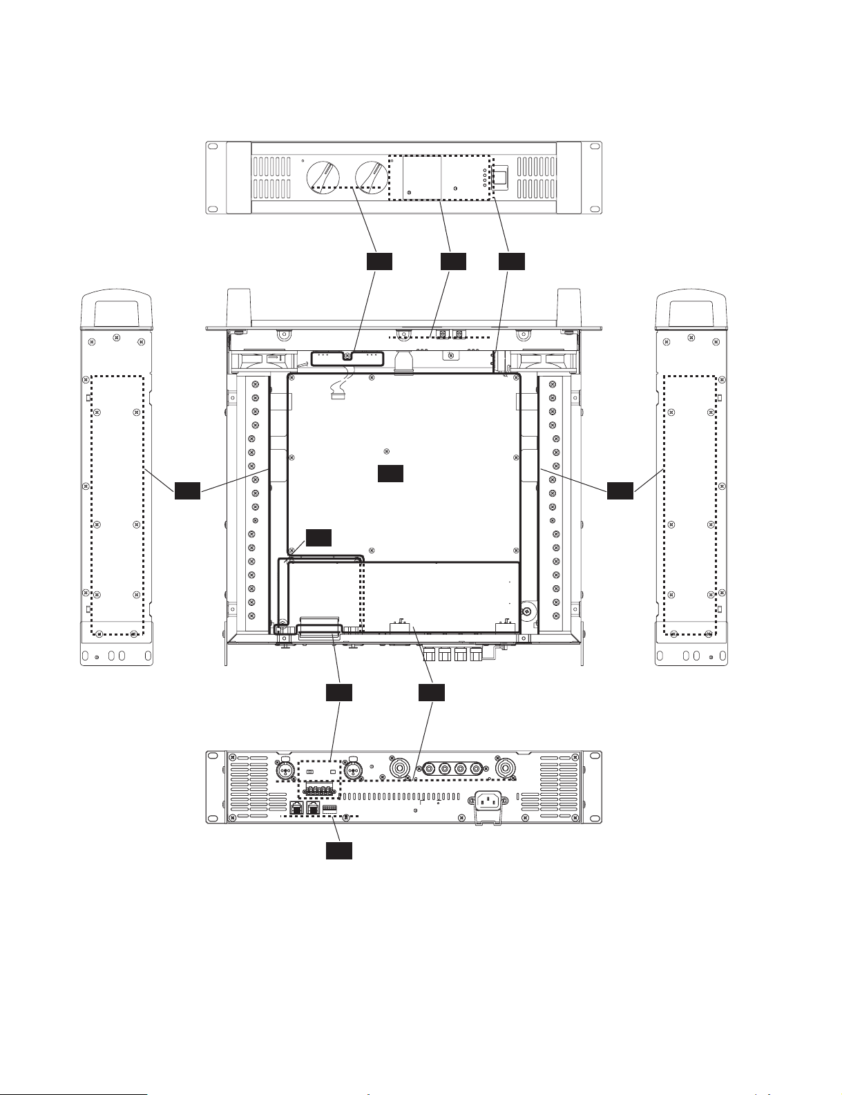
■ CIRCUIT BOARD LAYOUT(ユニットレイアウト)
• Front View(正面図)
• Side View
(側面図)
• Top View
(上面図)
PA
Bch
IN 4/5
IN 3/5 IN 2/5 PS 2/2
PS 1/2
•Side View
(側面図)
PA
Ach
IN 5/5
IN 1/5
• Rear View
(背面図)
IN 4/5
6
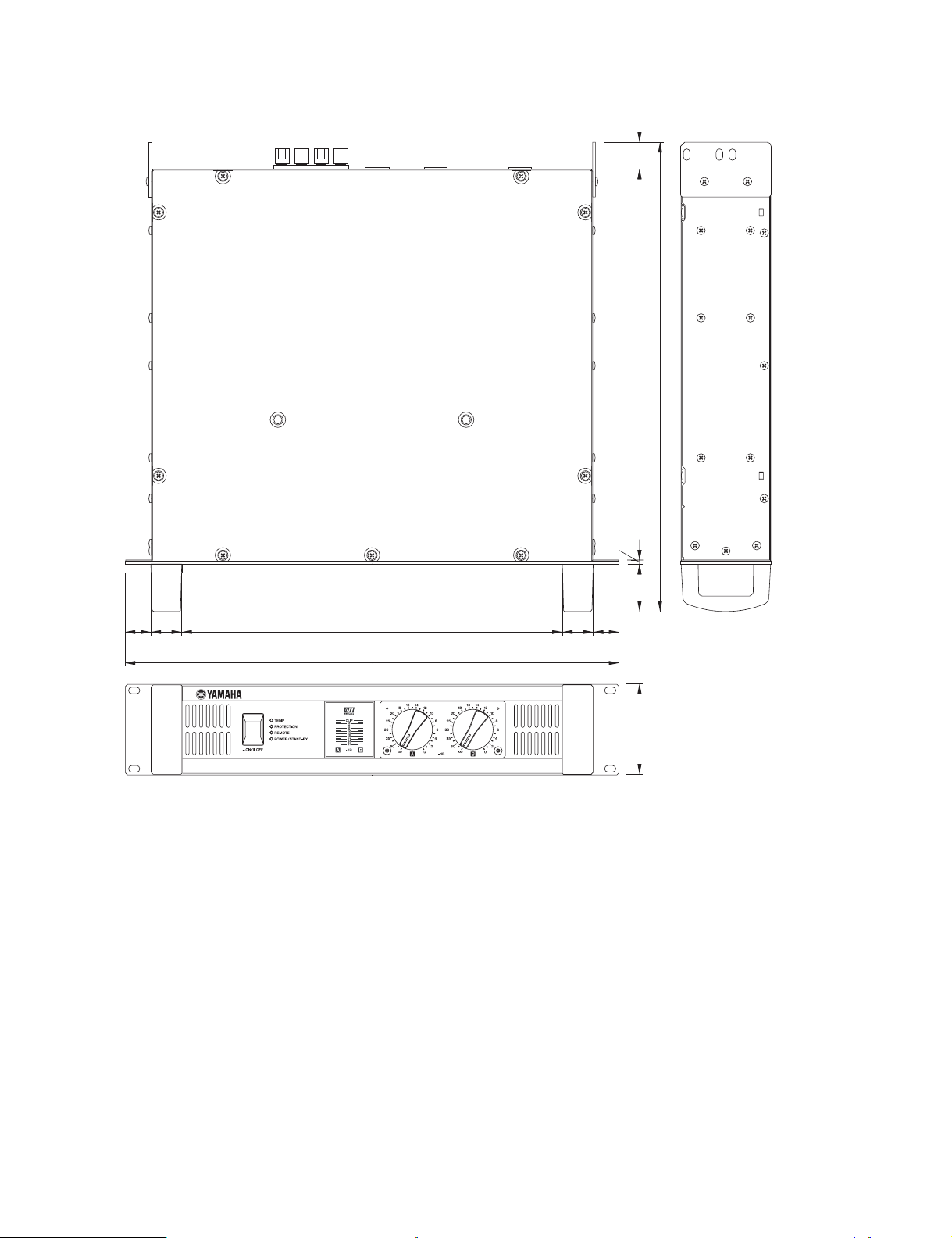
■ DIMENSIONS(寸法図)
PC6501N/PC4801N/PC3301N/PC2001N
26
380
456
25 30 370 30 25
480
POWER AMPLIFIER
PC 6501N
4
46
88
Units: mm
(単位)
7
PC6501N/PC4801N/PC3301N/PC2001N
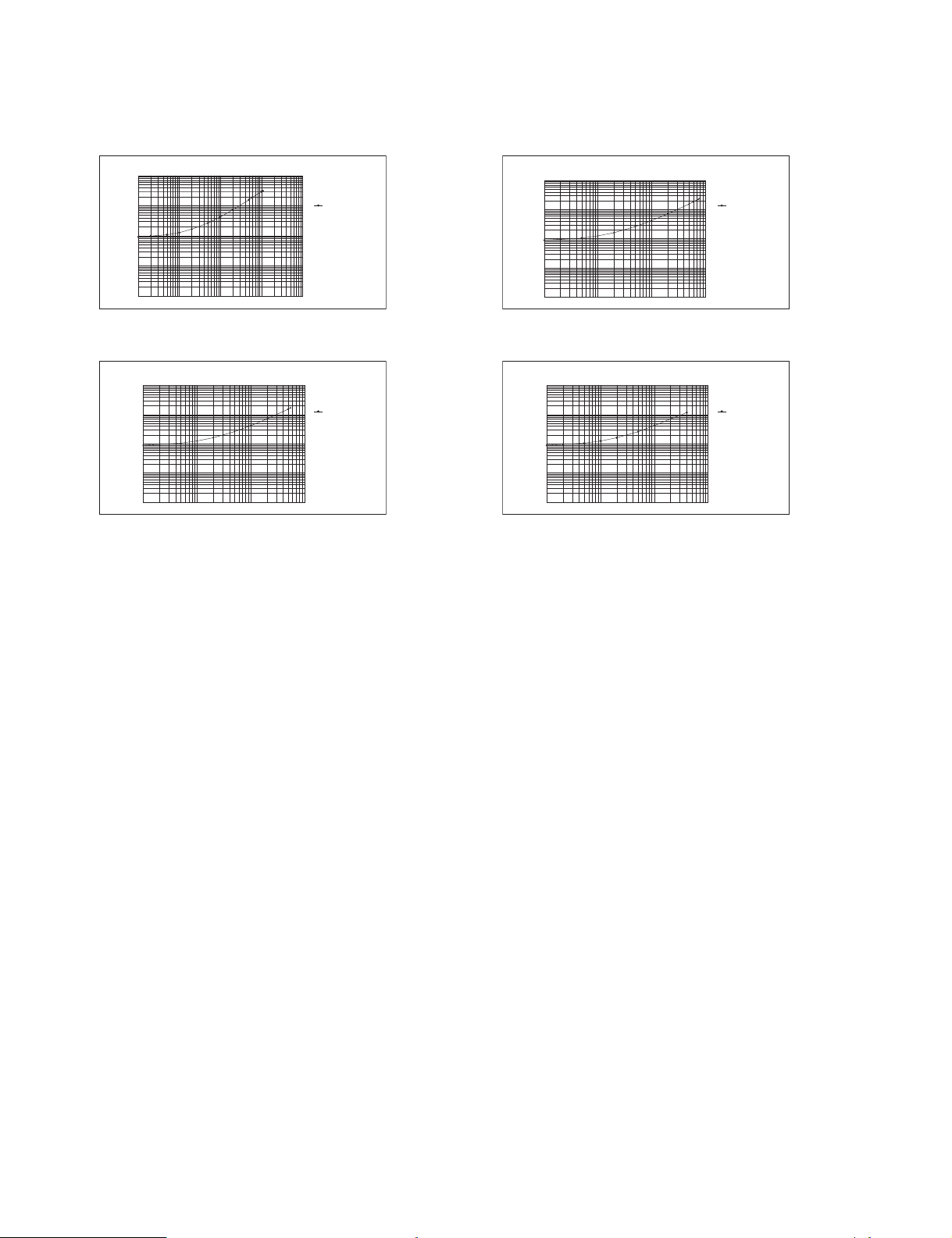
■ PERFORMANCE GRAPHS(特性図)
• PC6501N
PC6501N
10000
1000
100
10
Power consumption[W]
1
1 10 100 1000 10000
• PC3301N
PC3301N
10000
1000
100
10
Power consumption[W]
1
1 10 100 1000
Mode:STEREO
Both ch
Power
Consumption[W]
Output
Power[W]
Mode:STEREO
Both ch
Power
Consumption[W]
Output
Power[W]
• PC4801N
PC4801N
10000
1000
100
10
Power consumption[W]
1
1 10 100 1000
• PC2001N
PC2001N
10000
1000
100
10
Power consumption[W]
1
1 10 100 1000
Mode:STEREO
Both ch
Power
Consumption[W]
Output
Power[W]
Mode:STEREO
Both ch
Power
Consumption[W]
Output
Power[W]
8

■ DISASSEMBLY PROCEDURE(分解手順)
PC6501N/PC4801N/PC3301N/PC2001N
1. Top Cover (Time required: about 2 minutes)
1-1. Remove the nine (9) screws marked [280]. The top
cover can then be removed. (Fig. 1)
2. Rear Assembly (Time required: about 4 minutes)
2-1. Remove the top cover. (See Procedure 1.)
2-2. Remove the six (6) screws marked [240]. The rear
assembly can then be removed. (Fig. 2)
∗
With PC6501N of the J specification, remove the screw
marked [90]. (Fig.1)
[280]
[280] [280]
1. トップカバー(所要時間:約 2 分)
1-1. [280] のネジ 9 本 を 外 し、 ト ッ プカバーを外し ます。
(図1)
2. リア Assy(所要時間:約 4 分)
2-1. ト ッ プ カ バーを 外 し ま す。 (1 項参照 )
2-2. [240] のネジ 6 本 を 外 し、 リ ア Ass’ y を外 し ます。(図 2)
PC6501N(J)仕向は [90] のネジを外します。( 図 1)
∗
[30b]
PS 1/2
[90]
[40]
I/O Rock
[100]
IN 4/5
[280]
[30b]
[30]: Bind Head Tapping Screw-B 3.0X8 MFZN2BL (EP600190)+ バインド B タイト
[90]: Bind Head Screw 4.0X8 MFZN2BL (EG340360) + バインド小ネジ
[100]: Bind Head Tapping Screw-B 3.0X8 MFZN2BL (EP600190) + バインド B タイト
[280]: Bonding Tapping Screw-B 4.0X8 MFZN2BL (VR779900) ボンディング B タイト
[30a]
Fig.1 (図 1)
[330]
[240]
[240][240]
[240]: Bonding Tapping Screw-B 4.0X8 MFZN2BL (VR779900) ボンディング B タイト
[330]: Bind Head Tapping Screw-B 3.0X8 MFZN2BL (EP600190) + バインド B タイト
Fig.2 (図 2)
9
PC6501N/PC4801N/PC3301N/PC2001N
3. IN 1/5 Circuit Board (Time required: about 5 minutes)
3-1. Remove the top cover. (See Procedure 1.)
3-2. Remove the rear assembly. (See Procedure 2.)
3-3. Remove the two (2) screws marked [330] and then
remove the SP terminal cover. (Fig. 2)
3-4. Remove the one (1) screw marked [R70] , two (2)
screws marked [R80] , four (4) screws marked [R90]
and four (4) screws marked [R100]. The IN 1/5 circuit
board can then be removed. (Fig. 3)
4.
IN 4/5 Circuit Board (Time required: about 5 minutes
4-1. Remove the top cover. (See Procedure 1.)
4-2. Remove the rear assembly. (See Procedure 2.)
4-3. Remove the four (4) screws marked [30a]. The IN 4/5
circuit board can then be removed. (Fig. 1)
5. I
N 5/5 Circuit Board (Time required: about 3 minutes)
5-1. Remove the top cover. (See Procedure 1.)
5-2. Remove the two (2) screws marked [R60]. The IN 5/5
circuit board can then be removed. (Fig. 3)
3. IN1/5シート(所要時間:約 5 分)
3-1. ト ッ プ カバーを外 し ま す。 (1 項参照 )
3-2. リ ア Ass’ y を外 し ます。 (2 項参照 )
3-3. [330] のネ ジ 2本を外 し 、 S P タ ー ミ ナルカバーを外 し
ます。 (図2)
3-4. [R70] のネジ 1 本 と 、 [R80] のネジ 2 本、 [R90] のネ ジ 4
本、 [R100] のネ ジ 4 本を外 し 、 IN1/5 シ ー ト を外 し ま
す。 ( 図 3)
)
4. IN4/5シート(所要時間:約 5 分)
4-1. ト ッ プ カバーを外 し ま す。 (1 項参照 )
4-2. リ ア Ass’ y を外 し ます。 (2 項参照 )
4-3. [30a] のネジ 4本 を 外 し 、IN4/5 シー ト を外し ます。( 図 1)
5. IN5/5シート(所要時間:約 3 分)
5-1. ト ッ プ カバーを外 し ま す。 (1 項参照 )
5-2. [R60]のネジ2本 を 外 し 、IN5/5 シー ト を外し ます。(図3)
IN 1/5
[20] [20][R50]
[R90] [R90] [R70] [R100] [R100] [R10][R80][R60]
IN 5/5
[R60]: Pan Head Screw 2.6X6 MFZN2BL (VC990500)+ ナベ小ネジ
[R70]: Bonding Tapping Screw-B 3.0X8 MFZN2BL (VN413300) ボンディング B タイト
[R80]: Bind Head Tapping Screw-B 3.0X12 MFZN2BL (VQ074600)+ バインド B タイト
[R90]: Bind Head Tapping Screw-B 2.6X8 MFZN2BL (VB096700)+ バインド B タイト
[R100]: Flat Head Tapping 3.0X8 MFZN2BL (EP600790) +皿Bタイト
Fig.3 (図 3)
6. Front Panel Assembly
(Time required: about 4 minutes)
6-1. Remove the three (3) screws marked [210a] from the
side cover L, three (3) screws marked [210b] from the
side cover R and two (2) screws marked [220]. The
front panel assembly can then be removed. (Fig. 4)
10
6. フロントパネル Assy(所要時間:約 4 分)
6-1. サ イ ド カバー L [210a] の ネ ジ 3本 と サ イ ド カバー R
[210b] の ネ ジ 3 本 を 外 し 、 [220] のネ ジ 2本 を 外 し 、 フ
ロ ン ト パネル Ass’ y を 外 し ま す。 ( 図 4)
PC6501N/PC4801N/PC3301N/PC2001N
Side Cover R
(サイドカバーR)
[210b]
[190]
[185]
[185]: Flat Washer 4X9X0.8 MFZN2BL (VP367000) 平座金みがき丸
[190]: Bonding Tapping Screw-B 4.0X8 MFZN2BL (VR779900) ボンディング B タイト
[210]: Bonding Tapping Screw-B 4.0X8 MFZN2BL (VR779900) ボンディング B タイト
[220]: Bind Head Tapping Screw-B 3.0X8 MFZN2BL (EP600190)+ バインド B タイト
Fig.4 (図 4)
7. DC Fan (Time required: about 4 minutes)
7-1. Remove the top cover. (See Procedure 1.)
7-2. Remove the front panel assembly. (See Procedure 6.)
7-3. Remove the two (2) screws marked [F30] from the DC
fan and then remove the fan. Use the same for both
right and left fans. (Fig. 5)
[220]
PS 1/2
Side Cover L
(サイドカバーL)
[190]
[185]
IN 1/5
7. DC ファン(所要時間:約 4 分)
7-1. ト ッ プ カ バーを 外 し ま す。 (1 項参照 )
7-2. フ ロ ン ト パネル Ass’ y を外 し ます。 (6 項参照 )
7-3. DC フ ァ ン の [F30] のネ ジ 2 本を外し 、 フ ァ ン を外 し ま
す。 左右 と も同 じ 方法で外せ ます。 ( 図 5)
[210a]
8. Power Switch (Time required: about 8 minutes)
8-1. Remove the top cover. (See Procedure 1.)
8-2. Remove the front panel assembly. (See Procedure 6.)
8-3. Remove the DC fans. (See Procedure 7.)
8-4. Remove the four (4) screws marked [F180] and then
remove the two front covers. (Fig. 5)
8-5. Remove the six (6) screws marked [F150] and then
remove the front panel. (Fig. 6)
8-6. Remove the Power switch knob and the two (2)
screws marked [F40]. The power switch (PS 2/2
circuit board mount) can then be removed. (Fig. 6)
8-7. Remove the power switch from the PS 2/2 circuit
board.
[F180]
[F180][F30] [F30]
[F30]: Bind Head Screw 4.0X30 MFZN2BL (VT229100) + バインド小ネジ
[F180]: Bind Head Tapping Screw-B 3.0X8 MFZN2BL (EP600190)+ バインド B タイト
[F30][F30]
Fig.5 (図 5)
8. パワースイッチ(所要時間:約 8 分)
8-1. ト ッ プ カ バーを 外 し ま す。 (1 項参照 )
8-2. フ ロ ン ト パネル Ass’ y を外 し ます。 (6 項参照 )
8-3. DC フ ァ ン を外 し ます。 (7 項参照 )
8-4. [F180] のネ ジ 4 本を外し 、 フ ロ ン ト カバー印刷及びフ
ロ ン ト カバー処理を 2 ケ所外 し ま す。 ( 図 5)
8-5. [F150] のネジ 6 本 を 外 し、 フ ロ ン ト パネル を 外 し ま す。
(図6)
8-6. パ ワ ース イ ッ チ ノブを外 し 、 [F40] のネジ 2 本を外 し 、
パ ワ ース イ ッ チ (PS2/2 シー ト に マ ウ ン ト ) を 外 し ま
す。 ( 図 6)
8-7. PS2/2 シー ト か ら パ ワース イ ッ チを外し ます。
Front Cover(フロントカバー印刷)
PC 6501N
Front Cover(フロントカバー処理)
11
PC6501N/PC4801N/PC3301N/PC2001N
9. IN 2/5 Circuit Board (Time required: about 4 minutes)
9-1. Remove the top cover. (See Procedure 1.)
9-2. Remove the front panel assembly. (See Procedure 6.)
9-3. Remove the DC fans. (See Procedure 7.)
9-4. Remove the four (4) screws marked [F180] and then
remove the two front covers. (Fig. 5)
9-5. Remove the six (6) screws marked [F150] and then
remove the front panel. (Fig. 6)
9-6. Remove the two (2) screws marked [F70]. The IN 2/5
circuit board can then be removed. (Fig. 6)
10. IN 3/5 Circuit Board (Time required: about 4 minutes)
10-1. Remove the top cover. (See Procedure 1.)
10-2. Remove the front panel assembly. (See Procedure 6.)
10-3. Remove the DC fans. (See Procedure 7.)
10-4. Remove the two front covers. (See Step 9-4.)
10-5. Remove the front panel. (See Step 9-5.)
10-6. Remove the two (2) knobs of attenuation A/B and two
(2) hexagonal nuts. The IN 3/5 circuit board can then
be removed. (Fig. 6)
[F150]
9. IN2/5 シート(所要時間:約 4 分)
9-1. ト ッ プ カバーを外 し ま す。 (1 項参照 )
9-2. フ ロ ン ト パネル Ass’ y を外 し ます。 (6 項参照 )
9-3. DC フ ァ ン を外 し ます。 (7 項参照 )
9-4. [F180] の ネ ジ 4本を外し 、 フ ロ ン ト カバー印刷及び フ
ロ ン ト カバー処理を 2 ケ所外 し ま す。 ( 図 5)
9-5. [F150] のネジ 6本 を 外 し 、 フ ロ ン ト パネル を 外 し ま す。
(図6)
9-6. [F70] のネジ 2 本 を 外 し、 IN 2/5 シー ト を外し ます。
(図6)
10. IN3/5シート(所要時間:約 4 分)
10-1. ト ッ プカバーを外し ます。 (1 項参照 )
10-2. フ ロ ン ト パネル Ass’ y を外 し ま す。 (6 項参照 )
10-3. DC フ ァ ンを 外 し ま す。 (7 項参照 )
10-4. フ ロ ン ト カバー印刷及びフ ロ ン ト カバー処理を 2 ケ所
外し ま す。 (9-4. 項参照 )
10-5. フ ロ ン ト パネル を 外 し ま す。 (9-5. 項参照 )
10-6. ア ッ テ ネー タ ーA/B の ツ マ ミ 2 ケ と VR の六角ナ ッ ト 2
ケを外し、 IN 3/5シート を外します。 (図6)
PS 2/2 IN 3/5
[F60] [F80]
[F150]
[F40]: Bind Head Screw 3.0X6 MFZN2BL (EG330360) +バインド小ネジ
[F70]: Bind Head Tapping Screw-B 3.0X8 MFZN2BL (EP600190) +バインド B タイト
[F150]: Flat Head Screw 4.0X8 MFZN2BL (VA221200)+皿小ネジ
Fig.6 (図 6)
11. PA Unit (Time required: about 7 minutes)
11-1. Remove the rear assembly. (See Procedure 2.)
11-2. Remove the top cover. (See Procedure 1.)
11-3. Remove the nine (9) screws marked [190] and three
(3) screws marked [210]. The side cover and PA unit
can then be removed. Use the same method for both
A and B channels. (Fig. 4)
∗
Flat washers marked [185] are attached between the side
cover and PA unit. Take care not to lose flat washers
marked [185] when removing screws marked [190].
[F10]
Attenuation knob
(アッテネーターノブ)
Hexagonal nut
(六角ナット)
Power Switch knob
(パワースイッチノブ)
[F70][F40]
IN 2/5
11. PA ユニット(所要時間:約 7 分)
11-1. リ ア Ass’ y を外 し ます。 (2 項参照 )
11-2. ト ッ プカバーを外し ます。 (1 項参照 )
11-3. [190] のネジ 9 本と [210] のネ ジ 3 本を外 し 、 サイ ド カ
バーを外し、 PAユニ ッ ト を外し ます。 A、 B チャ ンネ
ルとも同じ方法で外れます。 (図4)
∗
PA ユニットとサイドカバーの間には、平座金 [185]があります。
[190]のネジを外すときは、[185]の平座金を紛失しないよう注意
してください。
12

PC6501N/PC4801N/PC3301N/PC2001N
12. PA Circuit Board (Time required: about 11 minutes)
12-1. Remove the top cover. (See Procedure 1.)
12-2. Remove the PA unit. (See Procedure 11.)
12-3. Remove the screws fixing the pair transistor, FET and
diode marked [P60] (27 screws for PC6501N, 25
screws for PC4801N, 23 screws for PC3301N, 21
screws for PC2001N), three (3) screws marked [P80]
and six (6) screws marked [P40]. The PA circuit board
can then be removed. (Fig. 7)
[P60] [P60][P80]
[P40]
12. PA シート(所要時間:約 11 分)
12-1. ト ッ プカバーを外し ます。 (1 項参照 )
12-2. PA ユニ ッ ト を外 し ます。 (11 項参照 )
12-3. ペアー ト ラ ン ジ ス タ ー、 FET と ダ イ オー ド の止めネ ジ
[P60] (PC6501N : 27 本、 PC4801N : 25本、 PC3301N :
23 本、 PC2001N : 21 本) と [P80] のネ ジ 3本、 [P40] の
ネジ6本を外し、PAシート を外します。 (図7)
PA5, PA3, PA2: not installed
PA3, PA2: not installed
PA2: not installed
[P40]
[P60] [P60][P80]
[P40]: Bind Head Screw 3.0X6 MFZN2BL (EG330360) +バインド小ネジ
[P60]: Bind Head Screw-SP 3.0X12 MFZN2Y (VB763800) +バインド小ネジ
[P80]: Bind Head Screw-SP 2.6X8 MFZN2Y (EG320240) +バインド小ネジ
Fig.7 (図 7)
13. PS Circuit Board (Time required: about 8 minutes)
13-1. Remove the top cover. (See Procedure 1.)
13-2. Remove the front panel assembly. (See Procedure 6.)
13-3. Remove the rear assembly. (See Procedure 2.)
13-4. Remove the eleven (11) screws marked [30b], one (1)
screw marked [100] and one (1) screw marked [90]
and then release the I/O lock marked [40]. The PS
circuit board can then be removed. (Fig. 1)
[40]: PC6501N (J) is not used.
PA5, PA3, PA2: not installed
PA3, PA2: not installed
PA2: not installed
13. PS シート(所要時間:約 8 分)
13-1. ト ッ プカバーを外し ます。 (1 項参照 )
13-2. フ ロ ン ト パネル Ass’ y を外 し ます。 (6 項参照 )
13-3. リ ア Ass’ y を外 し ます。 (2 項参照 )
13-4. [30b] のネジ 11 本 と [100] のネジ 1 本 と [90] の ネ ジ 1本
を外 し 、 [40] の I/O ロ ッ ク を 外 し 、 PS シー ト を 外 し ま
す。 (Fig.1)
[40]: PC6501N (J) は使用 し て い ません。
13
14
PC6501N/PC4801N/PC3301N/PC2001N
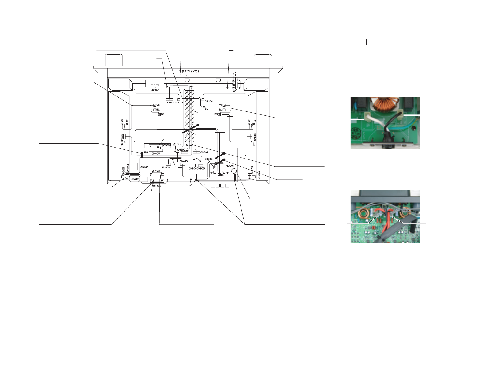
■ NOTES ON WIRING
Arrange the black and brown wires under the tube [250],
and fix the wires and tube with the cord holder [260].
Twist the black, yellow
and brown wires, then
connect the fasten
terminals to the circuit
board.
Fix the connector
assemblies [150] and
[F80] connected to CN201
and CN406 so that they
do not touch the heat sink
of the PA unit and the
parts on the PS circuit
board.
Wire the connector assembly
[140] connected to CN205 so
that it does not pass under the
screw hole of JK402.
Wire the connector assembly [140]
connected to CN205 so that it passes
between the connector assembly
[R50] and the rear panel.
Connector assembly PSW
[F80]
Fan Fan
[120]
[R50]
Bend the connector
assembly [R50] so that it
does not touch the top
panel.
[F60]
[110]
[250]
[160]
[150]
[140]
Refer to *3.
Fix the connector assemblies [150] and
[140] connected to CN201 and CN205
so that they do not loosen.
Twist the black, yellow
and brown wires, then
connect the fasten
terminals to the circuit
board. Then fix the
wires with the cord
holder [260].
Attach the tube to the
connector assemblies
so that they do not
touch the parts on the
PS circuit board, and fix
them with the cord
holder [260].
Refer to *4.
*1 The mark indicates the cord
holder.
*2 Attach the connector assemblies
[120] and [R50] with the
character upside.
*3 For PC6501N (J), connect the
black wire of the AC cord [60] to
CN111 and the white wire to
CN112.
CN112
*4 Run the connector assembly
[140] connected to CN609 and
CN610 through under two red
wires and one black wire, and fix
them with the cord holder [260].
CN111
CN610CN609
[110]: Connector Assembly PH&PH 9P 350L (VN667700)
[120]: Connector Assembly 37P 60mm P=1.25 (MF137060)
[140]: Connector Assembly IN (WD522000)
[150]: Connector Assembly IN3 (WD522100)
[160]: Connector Assembly TE (WD522300)
[250]: Tube BLACK D=18 (--)
[260]: Cord Holder BK-1 (CB069250)
[F60]: Connector Assembly PH&PH 11P 310L (WD521900)
[F80]: Connector Assembly ATT (--)
[R50]: Connector Assembly 35P 60mm P=1.25 (MF135060) *(--): Not available as spare parts.

■ 配線上の注意
黒、茶の線材をスミチューブ[250]の下に配置し、
インシュロックタイ[260]で固定します。
黒、黄、茶の線材は1〜2回
よじってからファストン端
子を接続します。
CN201、CN406に接続する束
線[150]および[F80]が
PAユニットのヒートシンクお
よびPSシート内の部品に接触
しないよう結束します。
CN205に接続する束線[140]が
JK402上のネジ穴の下を通過しな
いように配線します。
CN205に接続する束線[140]がカー
ド電線C&C[R50]とリアパネルの間
を通過するように配線します。
束線PSW
[F80]
DCファン DCファン
[120]
[R50]
[F60]
[110]
[250]
[160]
[150]
[140]
カード電線C&C[R50]
が天板に接触しないよう
に曲げておきます。
※3を参照してください。
CN201、CN205に接続する束線[150]およ
び[140]がたるまないように結束します。
黒、黄、茶の束線は1〜2回
よじってからファストン端
子を接続し、インシュロッ
クタイ[260]で固定しま
す。
この部分の束線がPSシート
内の部品に接触しないよう
にスミチューブを装着し、
インシュロックタイ
[260]で固定します。
※4を参照してください。
※1 図中のはインシュロックタイを
示しています。
※2 カード電線C&C[120]および
[R50]は文字面が上になるよう
取り付けます。
※3 PC6501N(J)では、電源コード
[60]の黒線をCN111、白線を
CN112に取り付けます。
CN112
※4 CN609、CN610に接続する束線
[140]は赤2本、黒1本の線の下
を通し、インシュロックタイ
[260]で固定します。
CN111
CN610CN609
PC6501N/PC4801N/PC3301N/PC2001N
15
[110]: Connector Assembly PH&PH 9P 350L (VN667700) 束線 #28
[120]: Connector Assembly 37P 60mm P=1.25 (MF137060) カード電線 C&C
[140]: Connector Assembly IN (WD522000) 束線 IN
[150]: Connector Assembly IN3 (WD522100) 束線 IN3
[160]: Connector Assembly TE (WD522300) 束線 TE
[250]: Tube BLACK D=18 (--) スミチューブ
[260]: Cord Holder BK-1 (CB069250) インシュロックタイ
[F60]: Connector Assembly PH&PH 11P 310L (WD521900) 束線 #28
[F80]: Connector Assembly ATT (--)束線 ATT
[R50]: Connector Assembly 35P 60mm P=1.25 (MF135060) カード電線 C&C ※ (--): サービス用部品として準備されていません。
PC6501N/PC4801N/PC3301N/PC2001N
■ LSI PIN DESCRIPTION(LSI端子機能表)
• HD64F7044F28V (X5719B00) CPU IN: IC801
PIN
NAME I/O FUNCTION
NO.
1
PE1/TIOC4C/DACK0/AH
PE15/TIOC4D/DACK1/IRQOUT
2
_____
I/O
Port E / MTU I/O / DMA transfer strobe / Address hold
I/O
Port E / MTU I/O / DMA transfer strobe / Interrupt request output
3 Vss I Ground 59 PD9/D9 I/O
4PC0/A0 O
5 PC1/A1 O 61 Vss I Ground
6PC2/A2 O 62PD7/D7 I/O
7PC3/A3 O 63PD6/D6 I/O
8PC4/A4 O 64PD5/D5 I/O
9 PC5/A5 O 65 Vcc I Power supply
10 PC6/A6 O 66 PD4/D4 I/O
11 PC7/A7 O 67 PD3/D3 I/O
12 PC8/A8 O 68 PD2/D2 I/O
Port C / Address bus
13 PC9/A9 O 69 PD1/D1 I/O
14 PC10/A10 O 70 PD0/D0 I/O
15 PC11/A11 O 71 Vss I Ground
16 PC12/A12 O 72 XTAL I Crystal oscillator
17 PC13/A13 O 73 MD3 I Mode set
18 PC14/A14 O 74 EXTAL I External clock
19 PC15/A15 O 75 MD2 I Mode set
20 PB0/A16 O Port B / Address bus 76 NMI I Non-maskable interrupt request
21 Vcc I Power supply 77 Vcc I Power supply
22 PB1/A17 O Port B / Address bus 78 MD1 I
23 Vss I Ground 79 MD0 I
________
_________
/POE0
________
________
/POE1
________
________
/POE2
________
_________
/POE3
_________
/A18/ BACK
_________
/A19/ BREQ
_________
/A20/ WAIT
_________
/A21/ADTRG
_____
_______________
________
________
_______
_______
___________
_______
/RAS
I/O
________
/CASL
________
/CASH
/RDWR
___________
___________
__________
____________
Port B / Interrupt request / Port output enable / Row address strobe
I/O
Port B / Interrupt request / Port output enable / Lower column address strobe
I/O
Port B / Interrupt request / Port output enable / Upper column address strobe
I/O
Port B / Interrupt request / Port output enable / DRAM read/write
I/O
Port B / Interrupt request / Address bus / Bus request acknowledge85PE0/TIOC0A/DREQ0
I/O
Port B / Interrupt request / Address bus / Bus request
I/O Port B / Interrupt request / Address bus / Wait 87
I/O
Port B / Interrupt request / Address bus / A/D conversion trigger input
O Port A / Read 90 Vss I Ground
O Watchdog time overflow 91 PF0/AN0 I
O Port A / Upper write 92 PF1/AN1 I
O Port A / Lower write 94 PF3/AN3 I
O
Port A / Chip select
O 97 AVss I Analog ground
________
I
________
______
______
_______
/IRQ1
Port A / MTU timer clock input / Interrupt request
I99PF7/AN7I
I/O
Port A / MTU timer clock input / Chip select
I/O 101 Vss I Ground
I/O
Port A / Serial clock / DMA transfer request / Interrupt request
PB2/IRQ0
24
PB3/IRQ1
25
PB4/IRQ2
26
27 Vss I Ground 83 PA15/CK O Port A / System clock
PB5/IRQ3
28
PB6/IRQ4
29
30
PB7/IRQ5
31
PB8/IRQ6
PB9/IRQ7
32
33 Vss I Ground 89
34 PA14/RD
35 WDTOVF
36 PA13/WRH
37 Vcc I Power supply 93 PF2/AN2 I
38 PA12/WRL
39 Vss I Ground 95 PF4/AN4 I
40 PA11/CS1
41 PA10/CS0
42
PA9/TCLKD/IRQ3
43
PA8/TCLKC/IRQ2
PA7/TCLKB/CS3
44
45
PA6/TCLKA/CS2
PA5/SCK1/DREQ1
46
47 PA4/TXD1 O Port A / Data transmission 103 Vcc I Power supply
48 PA3/RXD1 I Port A / Data reception 104
49
___________
PA2/SCK0/DREQ0
________
/IRQ0
I/O
Port A / Serial clock / DMA transfer request / Interrupt request
50 PA1/TXD0 O Port A / Data transmission 106
51 PA0/RXD0 I Port A / Data reception 107
52 PD15/D15 I/O
53 PD14/D14 I/O 109 Vss I Ground
Port D / Data bus
54 PD13/D13 I/O 110
55 Vss I Ground 111
56 PD12/D12 I/O Port D / Data bus 112
PIN
NAME I/O FUNCTION
NO.
57 PD11/D11 I/O
58 PD10/D10 I/O
Port D / Data bus
60 PD8/D8 I/O
Port D / Data bus
Port D / Data bus
Mode set
80 PLLVcc I PLL power supply
81 PLLCAP I PLL capacitance
82 PLLVss I PLL ground
_______
84 RES
86
PE1/TIOC0B/DRAK0
PE2/TIOC0C/DREQ1
88
PE3/TIOC0D/DRAK1
PE4/TIOC1A
I Power-on reset
____________
I/O Port E / MTU I/O / DMA transfer request
I/O
____________
Port E / MTU I/O / DREQ request acknowledgement
I/O Port E / MTU I/O / DMA transfer request
I/O
Port E / MTU I/O / DREQ request acknowledgement
I/O Port E / MTU I/O
Port F / Analog input
96 PF5/AN5 I
98 PF6/AN6 I
Port F / Analog input
100 AVcc I Analog power supply
102
PE5/TIOC1B
PE6/TIOC2A
105
PE7/TIOC2B
PE8/TIOC3A
PE9/TIOC3B
PE10/TIOC3C
108
PE11/TIOC3D
PE12/TIOC4A
PE13/TIOC4B/MRES
I/O Port E / MTU I/O
I/O
I/O
Port E / MTU I/O
I/O
I/O
I/O
I/O
Port E / MTU I/O
I/O
__________
I/O Port E / MTU I/O / Manual reset
16

■ IC BLOCK DIAGRAM(ICブロック図)
PC6501N/PC4801N/PC3301N/PC2001N
• NJM4558M (TE2) (X5804A00)
IN: IC601~IC606
• NJM2068M-D (TE2) (X3505A00)
IN: IC402~IC407, IC410
• M5238AFP (X6317A00)
IN: IC401
OP AMP
– +
8
7
6
5
+DC Voltage
Supply
Output B
Inverting
Input B
Non-Inverting
Input B
Output A
Inverting
Input A
Non-Inverting
Input A
Ground
1
2
– +
3
4
• TC7WH14FU (XY806A00)
IN: IC804
INVERTER
• NJM13600M (TE2) (X5042A00)
IN: IC409
OP AMP
– +
16
15
14
13
12
11
10
9
AMP BIAS INPUT B
DIODE BIAS B
+INPUT B
–INPUT B
OUTPUT B
V+
BUFFER INPUT B
BUFFER OUTPUT B
DIODE BIAS A
+INPUT A
–INPUT A
OUTPUT A
BUFFER INPUT A
BUFFER OUTPUT A
1AMP BIAS INPUT A
2
3
4
5
V–
6
7
8
– +
AB
• DS36276M (X2155A00)
IN: IC802
TRANSCEIVER
GND
1
2
3Y
2A
3
4
81A
Vcc
7
1Y
6
3A
5
2Y
• UC3525AN (X5952A00)
PS: IC101
REGULATOR
V
16
REF
15
+V
IN
14
OUTPUT B
13
V
C
12
GROUND
11
OUTPUT A
10
SHUTDOWN
9
COMPENSATION
N.I. INPUT
SYNC
OSC. OUTPUT
DISCHARGE
SOFT-START
1INV. INPUT
2
3
4
C
5
T
6
R
T
7
8
GROUND
SYNC
COMPENSATION
INV. INPUT
N.I. INPUT
CC
1
RO
RE
2
3
DE
DI
OSC
V
REF
OUT
16 4
Reference
15+V
IN
Regulator
12
3
R
6
T
5
C
T
7DISCHARGE
9
1
2
8SOFT-START
10SHUTDOWN
3 kΩ
OSC
Error
Amp
To Internal
circurity
UVLO
Lockout
Flip
Flop
COM
V
REF
50 µA
5 kΩ
R
S
PWM
Latch
S
NOR
NOR
D
4
V
8
R
DO/RI
7
6
DO/RI
GND
5
V
13
C
11
OUTPUT A
14
OUTPUT B
17
PC6501N/PC4801N/PC3301N/PC2001N
• TC9413AP (X2101A00)
IN: IC408
VOLUME
1V
SS
2
OUT
3
IN
L-ch
A-GND
CS1
GND
4
NC
5
6
7
8
CK
16
15
14
13
12
11
10
9
•IR2110 (X2382A00)
PS: IC102
DRIVER
COM
VCC
1LO
2
3
4
5
VS
6
VB
7
HO
14
13
12
11
10
9
8
DD
V
OUT
IN
NC
A-GND
CS2
STB
DATA
VSS
LIN
SD
HIN
VDD
R-ch
SS
V
Level
shift
circuit
R
R
Data latch
Q
S
S
Q
1 16
L-ch
circuit
Shift register (13bit)
Strobe generation circuit
2
OUT OUT
3
IN
L-ch
VDD
HIN
SD
LIN
VSS
4
NC
5
A-GND
6
CS1
GND
7
8
CK
9
10
11
14
15
VDD/VCC
LEVEL
SHIFT
VDD/VCC
LEVEL
SHIFT
V
DD
R-ch
Data latch
circuit
PULSE
PULSE
GEN
GEN
Level
shift
circuit
HV
LEVEL
SHIFT
15
IN
14
R-ch
13
NC
A-GND
12
CS2
11
10
STB
9
DATA
6
UV
DETECT
PULSE
FILTER
UV
DETECT
DELAY
R
Q
R
S
VB
7
HO
5
VS
3
CC
V
LO
1
COM
2
• LB1409M (X0654A00)
IN: IC701, IC702
LED DRIVE
1VCC
2
Vref1
+
3
IN
V
–
4
V
IN
OUT
5
GND
6
D1
7
8D2
18
13, 12, 11, 10, 9, 8
16
Vref2
D9
15
D8
14
D7
13
D6
12
11
D5
D4
10
9
D3
+
3
VIN
–
4
V
IN
5 6
OUT
Vref 1 Vref 2V
2 1
CC
16 15
R10
R20
10K
5
GND
D9
4.69K
R9
–
COM
+
98 1
3.31K
–
+
R8
COM
R7(2.34K), R6(1.66K), R5(1.17K)
R4(830), R3(586), R2(414)
D8 D1
14 7
–
+
1K
R1
COM

■ CIRCUIT BOARDS(シート基板図)
•CONTENTS(目次)
IN 1/5 Circuit Board (X5707B0) ....................................................... 20
IN 2/5 Circuit Board (X5707B0) ....................................................... 22
IN 3/5 Circuit Board (X5707B0) ....................................................... 22
IN 4/5 Circuit Board (X5707B0) ....................................................... 23
IN 5/5 Circuit Board (X5707B0) ....................................................... 23
PA Circuit Board (X5704B0) ............................................................ 24
PS 1/2 Circuit Board (X5692B0) ...................................................... 26
PS 2/2 Circuit Board (X5692B0) ...................................................... 26
PS 1/2 Circuit Board (X5692C0) ...................................................... 28
PS 2/2 Circuit Board (X5692C0) ...................................................... 28
Note: See parts list for details of circuit board component parts.
注:シートの部品詳細はパーツリストをご参照ください。
PC6501N/PC4801N/PC3301N/PC2001N
19
PC6501N/PC4801N/PC3301N/PC2001N
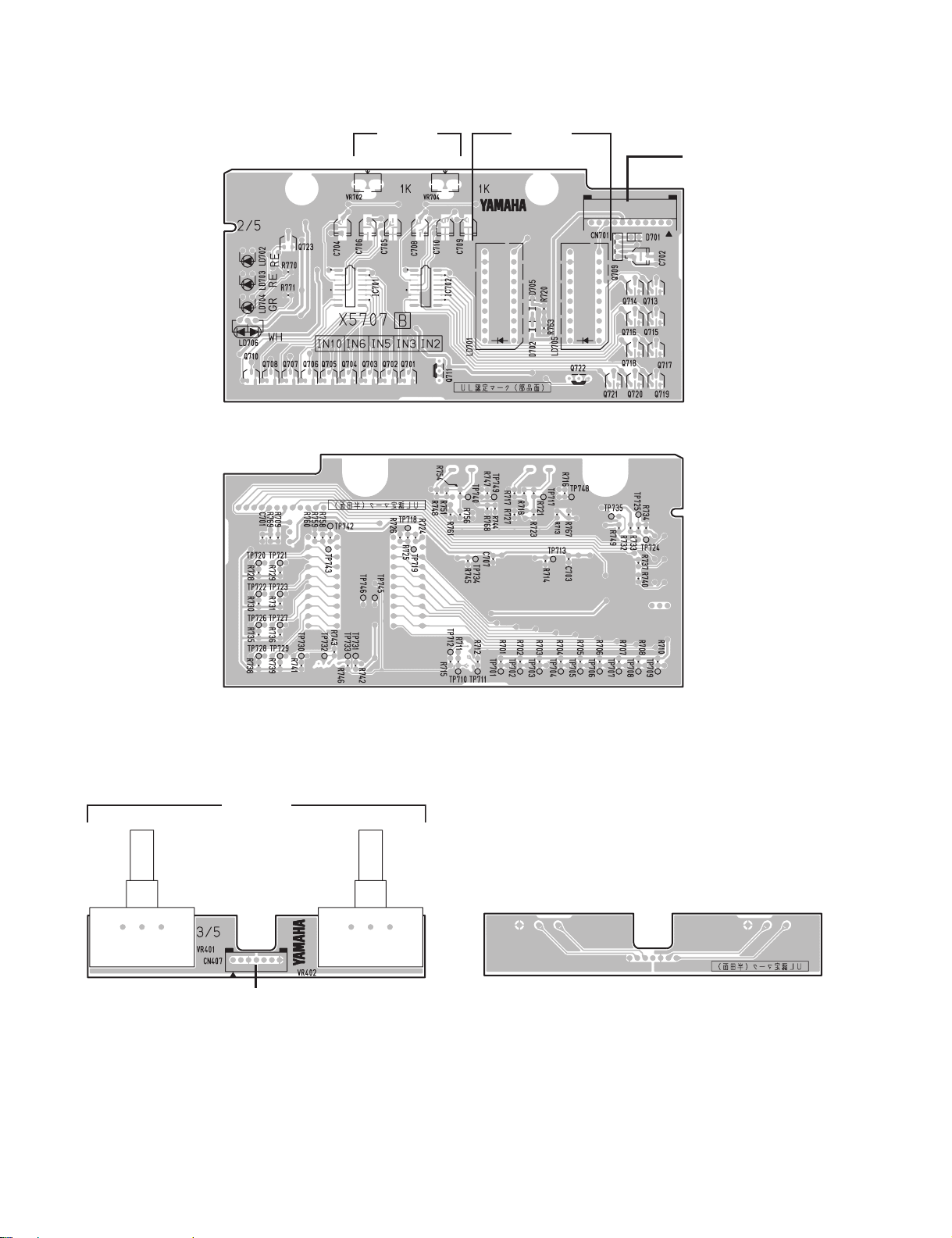
• IN 1/5 Circuit Board (PC6501N: IN6, PC4801N: IN5, PC3301N: IN3, PC2001N: IN2)
from PS6 1/2-W102
from PA ACH-CN205
from PA ACH-W204
A2 B2
SPEAKERS
A1 B1
OUTPUT
+
+
A
––
from PA BCH-W204
from PA BCH-CN205
GND
to PA ACH-CN202
to PA BCH-CN202
to IN 2/5-CN701
B
A'
20
B'
IN: 2LP-X5707B0
PC6501N/PC4801N/PC3301N/PC2001N
A
from PA ACH-CN201
from PA BCH-CN201 to IN 5/5-CN401
GND
AB
to IN 3/5-CN407
A'
to PS 1/2-CN102
to IN 4/5-CN801
Component side(部品側)
B
B'
IN: 2LP-X5707B0
Pattern side(パターン側)
21
PC6501N/PC4801N/PC3301N/PC2001N
• IN 2/5 Circuit Board
TEMP
PROTECT
REMOTE
POWER/STAND-BY
LEVEL
METER
ADJ.
AB
AB
LEVEL
METER
to IN 1/5-CN601
Component side(部品側)
• IN 3/5 Circuit Board
VOLUME
AB
to IN 1/5-CN406
Pattern side(パターン側)
Pattern side(パターン側)
Component side(部品側)
IN: 2LP-X5707B0
22

PC6501N/PC4801N/PC3301N/PC2001N
• IN 4/5 Circuit Board • IN 5/5 Circuit Board
to IN 1/5-CN405
AMP ID
12
DATA PORT
Component side(部品側)
CHANNEL INPUT
MODEHPF 20 Hz
from IN 1/5-CN402
Component side(部品側)
Pattern side(パターン側)
IN: 2LP-X5707B0
Pattern side(パターン側)
23
PC6501N/PC4801N/PC3301N/PC2001N
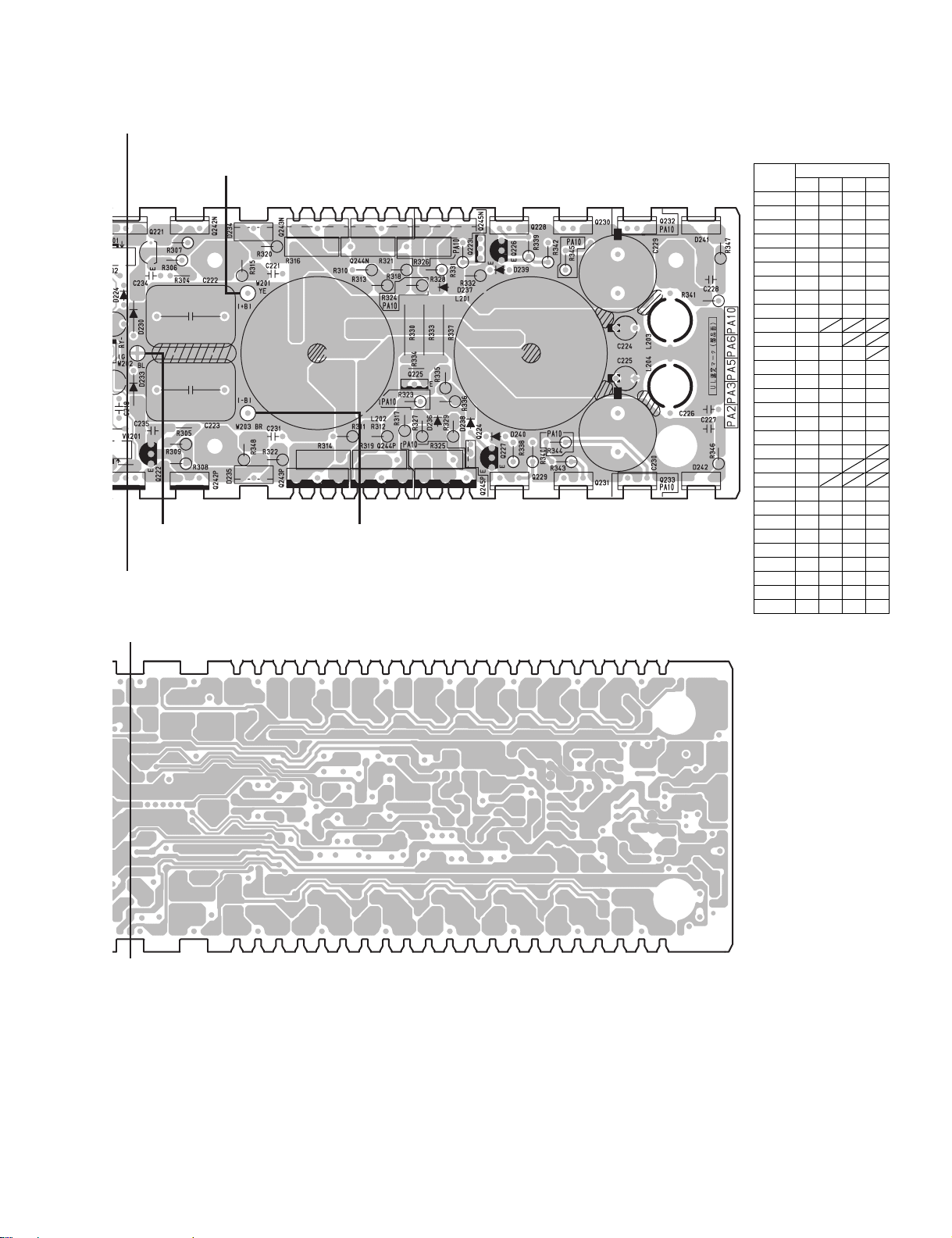
• PA Circuit Board (PC6501N: PA6, PC4801N: PA5, PC3301N: PA3, PC2001N: PA2)
PA ACH:
from IN
1/5-CN609
PA BCH:
from IN
1/5-CN610
OFFSET ADJ.
PA ACH:
from IN
1/5-CN403
PA BCH:
from IN
1/5-CN404
IDLING ADJ. B
PA ACH: from IN 1/5-CN603
PA BCH: from IN 1/5-CN604
N.C
Q235N Q236N Q237N Q238N Q239N Q240N Q234N IC201
N.C
Q235P Q236P Q237P Q238P Q239P Q240P Q234P Q212
PA ACH: to IN 1/5-CN605
PA BCH: to IN 1/5-CN608
IDLING ADJ. A
C
C'
D'
D
24
PA: 2LP-X5704B0
C
PA ACH: to PS 1/2-CN105
PA BCH: to PS 1/2-CN108
Q242N Q243N Q244N Q228 Q230 D241
Q242P D235 Q243P Q244P Q229 Q231 D242
PA ACH: to PS 1/2-CN106
PA BCH: to PS 1/2-CN109
C'
PA ACH: to PS 1/2-CN107
PA BCH: to PS 1/2-CN110
PC6501N/PC4801N/PC3301N/PC2001N
• Following semi-conductors are
installed for the PA unit.
(下記半導体は PA ユニ ッ ト で
取付 さ れます。)
Circuit board
ref.
PA6 PA5 PA3 PA2
○○○○
D242
○○○○
Q231
○○○○
Q229
○○○○
Q244P
○○○○
Q243P
○○○○
D235
○○○○
Q242P
○○○○
Q212
○○○○
Q234P
○
Q240P
○○
Q239P
○○○
Q238P
○○○○
Q237P
○○○○
Q236P
○○○○
Q235P
○○○○
Q235N
○○○○
Q236N
○○○○
Q237N
○○○
Q238N
○○
Q239N
○
Q240N
○○○○
Q234N
○○○○
IC201
○○○○
Component side(部品側)
Q242N
D234
Q243N
Q244N
Q228
Q230
D241
○○○○
○○○○
○○○○
○○○○
○○○○
○○○○
D'
D
Pattern side(パターン側)
PA: 2LP-X5704B0
25
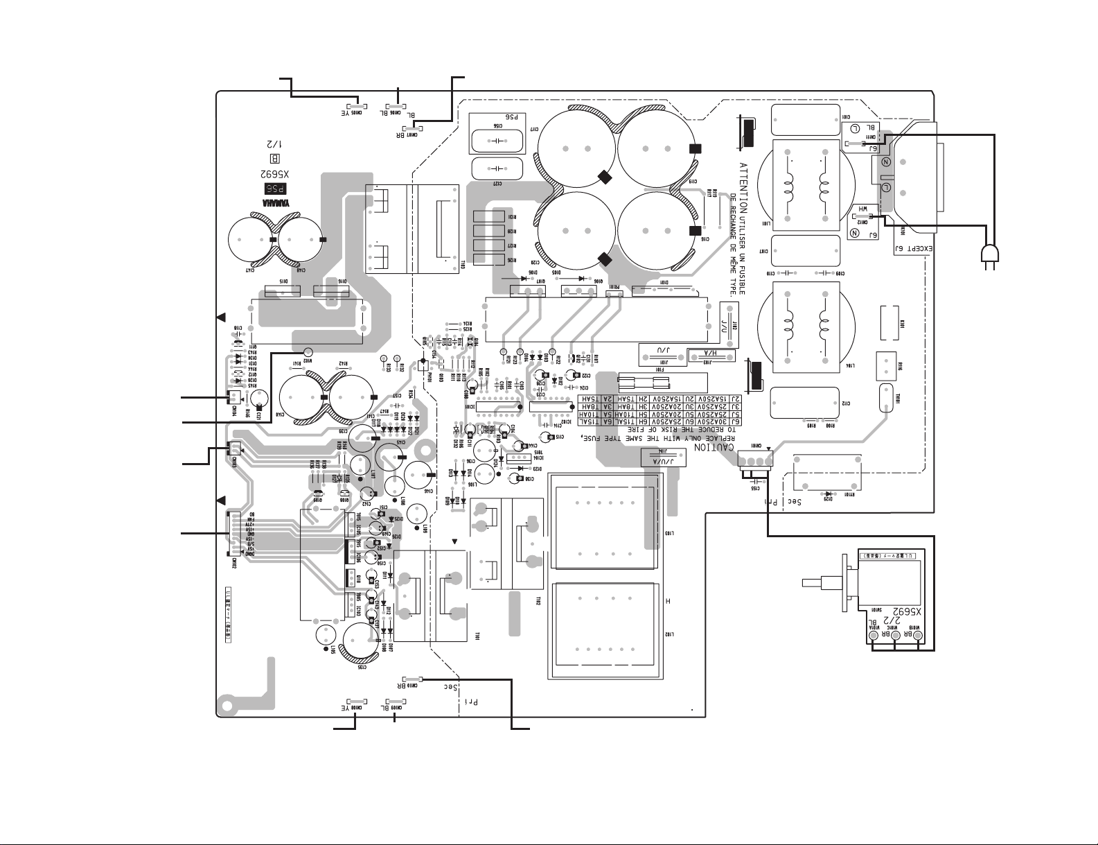
26
<B version (X5692B0)>
from PA ACH-W201
from FAN ACH
to IN 1/5-CN606
PC6501N/PC4801N/PC3301N/PC2001N
• PS 1/2 Circuit Board (PC6501N: PS6, PC4801N: PS5, PC3301N:PS3, PC2001N: PS2)
from PA ACH-W203from PA ACH-W202
AC IN
PC6501N (J)
from FAN BCH
to IN 1/5-CN602
PS: 2LP-X5692B0
• PS 2/2 Circuit Board
Component side(部品側)
from PA BCH-W202from PA BCH-W201
from PA BCH-W203
POWER
ON/OFF
(部品側)
Component side
• PS 2/2 Circuit Board • PS 1/2 Circuit Board
PC6501N/PC4801N/PC3301N/PC2001N
Pattern side(パターン側)
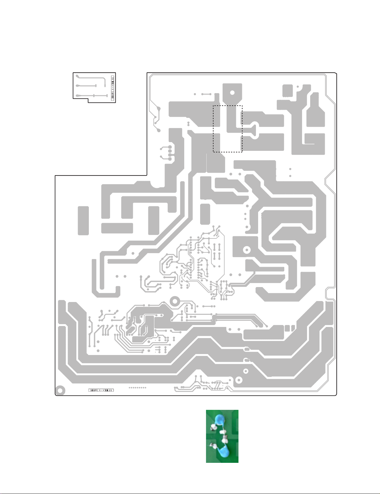
※
※ The capacitors [C158] and [C159] are attached in the dotted
area shown above (U, V, T models).
※ 上記点線部には規格認定コン [C158][C159] が裏付けされています(U、
V、T モデル)。
PS: 2LP-X5692B0
Pattern side(パターン側)
<B version (X5692B0)>
27
Loading...