


FT-1900R
Table of contents
 Loading...
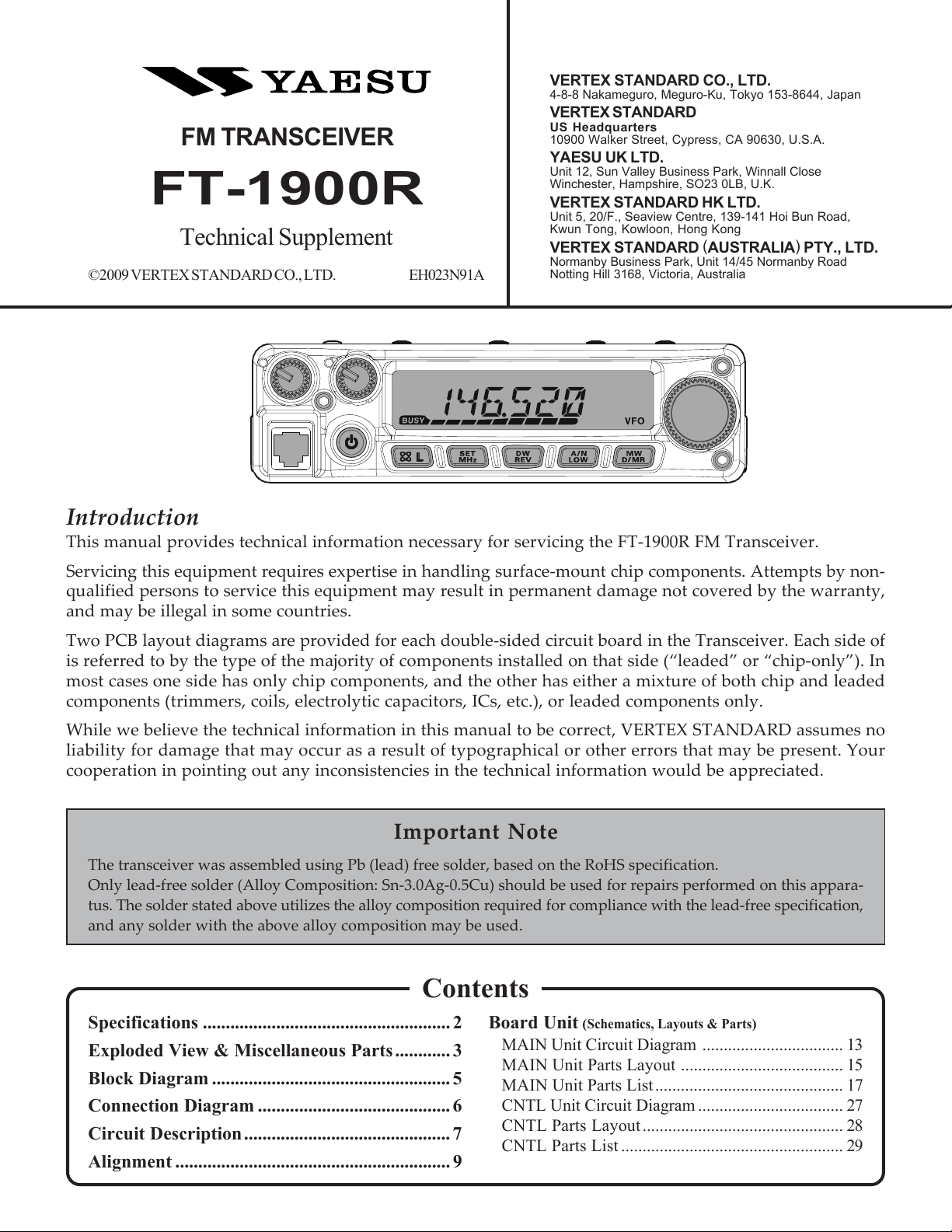
1
Introduction
This manual provides technical information necessary for servicing the FT-1900R FM Transceiver.
Servicing this equipment requires expertise in handling surface-mount chip components. Attempts by non-
qualified persons to service this equipment may result in permanent damage not covered by the warranty,
and may be illegal in some countries.
Two PCB layout diagrams are provided for each double-sided circuit board in the Transceiver. Each side of
is referred to by the type of the majority of components installed on that side (“leaded” or “chip-only”). In
most cases one side has only chip components, and the other has either a mixture of both chip and leaded
components (trimmers, coils, electrolytic capacitors, ICs, etc.), or leaded components only.
While we believe the technical information in this manual to be correct, VERTEX STANDARD assumes no
liability for damage that may occur as a result of typographical or other errors that may be present. Your
cooperation in pointing out any inconsistencies in the technical information would be appreciated.
©2009 VERTEX STANDARD CO., LTD. EH023N91A
Technical Supplement
Specifications ...................................................... 2
Exploded View & Miscellaneous Parts ............ 3
Block Diagram .................................................... 5
Connection Diagram .......................................... 6
Circuit Description............................................. 7
Alignment ............................................................ 9
Contents
Board Unit (
Schematics, Layouts & Parts
)
MAIN Unit Circuit Diagram ................................. 13
MAIN Unit Parts Layout ...................................... 15
MAIN Unit Parts List............................................ 17
CNTL Unit Circuit Diagram .................................. 27
CNTL Parts Layout............................................... 28
CNTL Parts List .................................................... 29
FM TRANSCEIVER
FT-1900R
VERTEX STANDARD CO., LTD.
4-8-8 Nakameguro, Meguro-Ku, Tokyo 153-8644, Japan
VERTEX STANDARD
US Headquarters
10900 Walker Street, Cypress, CA 90630, U.S.A.
YAESU UK LTD.
Unit 12, Sun Valley Business Park, Winnall Close
Winchester, Hampshire, SO23 0LB, U.K.
VERTEX STANDARD HK LTD.
Unit 5, 20/F., Seaview Centre, 139-141 Hoi Bun Road,
Kwun Tong, Kowloon, Hong Kong
VERTEX STANDARD
(
AUSTRALIA
)
PTY., LTD.
Normanby Business Park, Unit 14/45 Normanby Road
Notting Hill 3168, Victoria, Australia
Important Note
The transceiver was assembled using Pb (lead) free solder, based on the RoHS specification.
Only lead-free solder (Alloy Composition: Sn-3.0Ag-0.5Cu) should be used for repairs performed on this appara-
tus. The solder stated above utilizes the alloy composition required for compliance with the lead-free specification,
and any solder with the above alloy composition may be used.

2
Specifications
General
Frequency Range: Tx 144 - 146 MHz or 144 - 148 MHz
Rx 144 - 146 MHz or 136 - 174 MHz
Channel Step: 5/10/12.5/15/20/25/50/100 kHz
Standard Repeater Shift: ±600 kHz
Frequency Stability: Better than ±10 ppm [–4 °F to +140 °F (–20 °C to +60 °C)]
Modes of Emission: F2D/F3E
Antenna Impedance: 50 Ohms, unbalanced
Supply voltage: 13.8 V DC ±15%, negative ground
Current Consumption (typical): Rx: less than 0.7 A, less than 0.3 A (squelched)
Tx: 10 A (55 W) /7 A (25 W) /5 A (10 W) /4 A (5 W)
Operating Temperature Range: –4° F to +140° F (–20° C to +60° C)
Case Size (WxHxD): 5.5” x 1.6” x 5.7” (140 x 40 x 146 mm) (w/o knobs)
Weight (Approx.): 2.6 lb (1.2 kg)
Transmitter
Output Power: 55 W/25 W/10 W/5 W
Modulation Type: Variable Reactance
Maximum Deviation: ±5 kHz/±2.5 kHz
Spurious Radiation: Better than –60 dB
Microphone Impedance: 2000 Ohms
Receiver
Circuit Type: Double Conversion Superheterodyne
Ifs: 21.7 MHz & 450 kHz
Sensitivity (for 12dB SINAD): Better than 0.2 µV
Selectivity (–6/–60dB): 12 kHz/28 kHz
IF Rejection: Better than 70 dB
Image Rejection: Better than 70 dB
Maximum AF Output: 3 W into 4 Ohms @10 % THD
Specifications subject to change without notice or obligation. Specifications guaranteed only within Amateur band.
Frequency ranges and functions will vary according to transceiver version; check with your dealer.
3
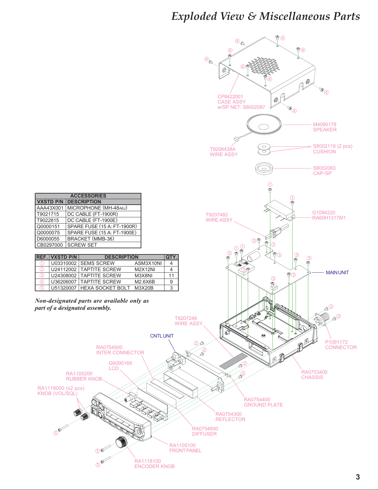
Exploded View & Miscellaneous Parts
g
c
d
e
f
g
d
d
d
c
c
c
f
f
f
f
f
f
f
f
e
e
e
e
e
e
e
e
e
e
M4090178
SPEAKER
Non-designated parts are available only as
part of a designated assembly.
S8002063
CAP-SP
RA1105100
FRONT PANEL
RA1105200
RUBBER KNOB
G6090169
LCD
RA0754500
INTER CONNECTOR
RA0754600
DIFFUSER
CNTL UNIT
MAIN UNIT
RA0754400
GROUND PLATE
RA0753400
CHASSIS
RA1118100
ENCODER KNOB
RA1118000 (x2 pcs)
KNOB (VOL/SQL)
RA0754300
REFLECTOR
P1091172
CONNECTOR
G1094220
RA60H1317M1
T9207482
WIRE ASSY
CP8422001
CASE ASSY
w/SP NET: S8002087
DESCRIPTION
MICROPHONE
(
MH-48A6J
)
DC CABLE
(
FT-1900R
)
DC CABLE
(
FT-1900E
)
SPARE FUSE
(
15 A: FT-1900R
)
SPARE FUSE
(
15 A: FT-1900E
)
BRACKET
(
MMB-36
)
SCREW SET
VXSTD P/N
AAA43X001
T9021715
T9022815
Q0000151
Q0000075
D6000055
CB0297000
ACCESSORIES
REF.
c
d
e
f
g
QTY.
4
4
11
9
3
DESCRIPTION
SEMS SCREW ASM3X10NI
TAPTITE SCREW M2X12NI
TAPTITE SCREW M3X8NI
TAPTITE SCREW M2.6X6B
HEXA SOCKET BOLT M3X20B
VXSTD P/N
U03310002
U24112002
U24308002
U36206007
U51320007
T9207248
WIRE ASSY
S8002118 (2 pcs)
CUSHION
T9206438A
WIRE ASSY
g

4
Note
5
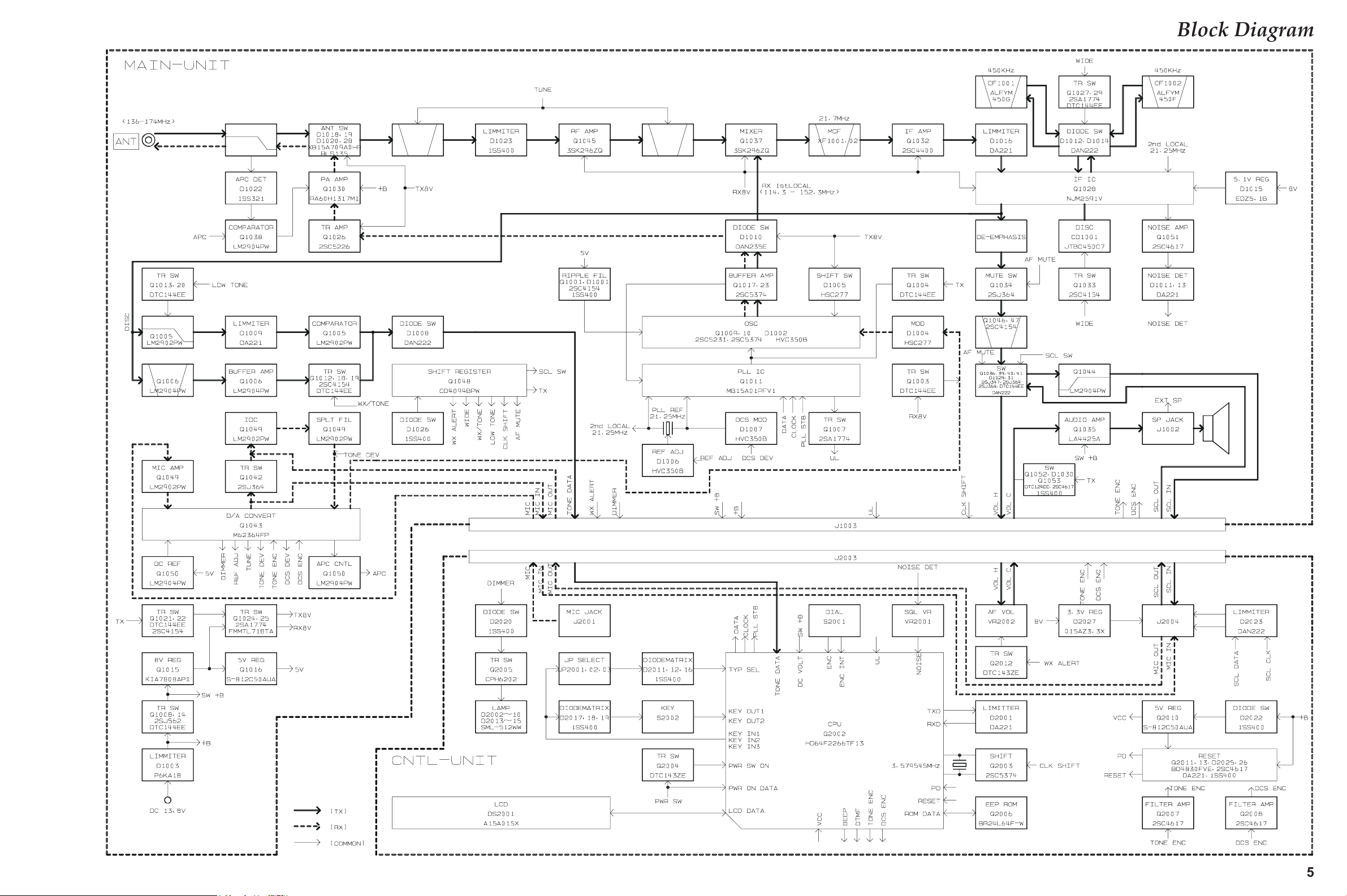
Block Diagram
6
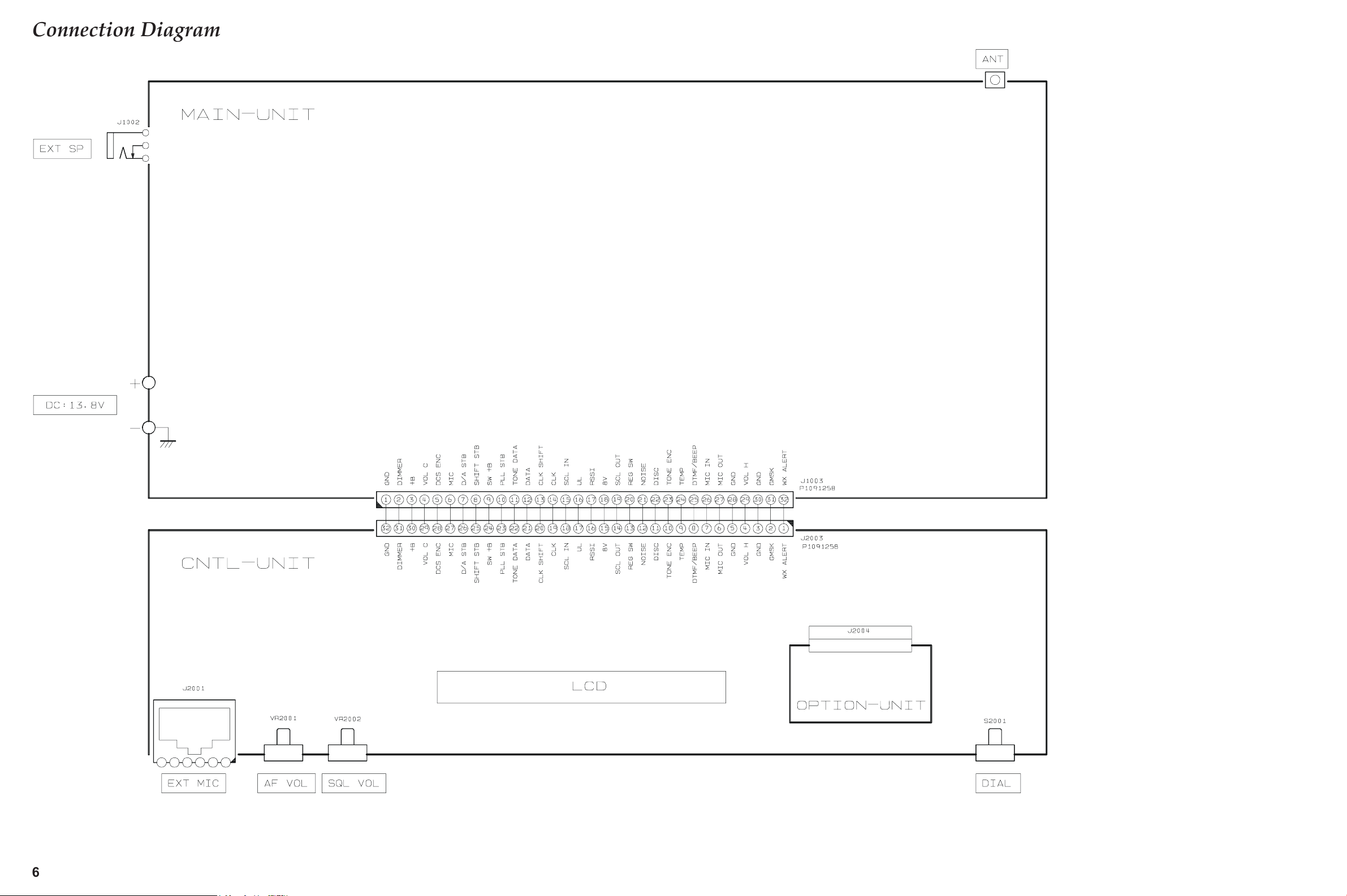
Connection Diagram
7
Circuit Description
Receive Signal Path
Incoming RF signal is from the antenna jack is de-
livered to the Main Unit and passed through the low-
pass filter network consisting capacitors C1213,
C1236, C1239, & C1241 and coils L1017, L1018, &
L1019, antenna switching diode D1020 and D1028
(both RLS135), and varactor-tuned band-pass filter
consisting of capacitors C1248, C1249, C1250, C1251,
C1252, & C1268, coils L1020, L1021, & L1024, and
diodes D1024 and D1025 (both HVC350B), before
delivery to the RF amplifier Q1045 (3SK296ZQ). The
amplified RF signal is passed through the another
varactor-tuned band-pass filter consisting of capac-
itors C1198, 1199, 1200, & 1218, coils L1012 and L1015,
and diodes D1017 and D1021 (both HVC350B), then
applied to the 1st mixer Q1037 (3SK296ZQ) along
with the first local signal from the PLL circuit.
The first local signal is generated between 114.3 MHz
and 152.3 MHz by the VCO, which consists of Q1009
(2SC5231) and varactor diode D1002 (HVC350B)
according to the receiving frequency.
IF and Audio Circuits
The 21.7 MHz first IF signal is applied to the mono-
lithic crystal filters XF1001 and XF1002 which strip
away unwanted mixer products, and the IF signal is
applied to the first IF amplifier Q1032 (2SC4400).
The amplified first IF signal is then delivered to the
FM IF subsystem IC Q1028 (NJM2591V), which con-
tains the second mixer, limiter amplifier, noise am-
plifier, and FM detector.
The second local signal is generated by 21.25 MHz
crystal X1001, produces the 450 kHz second IF sig-
nal when mixed with first IF signal within Q1028
(NJM2591V).
The 450 kHz second IF signal is applied to the ce-
ramic filter CF1001 (for Narrow FM) or CF1002 (for
Wide FM) which strip away unwanted mixer prod-
ucts to the ceramic discriminator CD1001 which re-
moves any amplitude variations in the 450 kHz IF
signal before detection of speech.
The detected audio from the Q1028 (NJM2591V)
passes through the de-emphasis circuit consisting
of resistors R1082 & R1113, and capacitors C1120 &
C1122, to the audio mute gate Q1034 (2SJ364)
The audio signal passes through a band-pass filter
consisting of Q1046 and Q1047 (both 2SC4154), and
the audio mute gate Q1039 (2SJ347), to the audio
VR which adjusts the audio sensitivity to compen-
sate for audio level variations. The adjusted audio
signal is delivered to the audio amplifier Q1035
(LA4425A) which provides up to 3 Watts, to the ex-
ternal speaker jack or a 4-Ohm loudspeaker.
Squelch Control
When no carrier received, the noise signal from
Q1028 (NJM2591V) is amplified by Q1051
(2SC4617), and is detected by D1011 and D1013
(both DA221). The resulting DC voltage passes
through the SQL knob to main CPU Q2002
(HD64F2266TF13). While no carrier is received,
main CPU Q2002 (HD64F2266TF13) control Q1048
(CD4094BPWR), thus, audio mute gate Q1034
(2SJ364) and Q1039 (2SJ347) turns “OFF” to dis-
able the audio output from the speaker.
Transmit Signal Path
The speech signal from the microphone is amplified
by Q1049 (LA2902PWR). The amplified speech sig-
nal is subjected to the low-pass filter network Q1049
(LA2902PWR) to deviation controlled by Q1043
(M62364FP).
The adjusted speech signal from Q1043 (M62364FP)
is delivered to VCO Q1009 (2SC5231) which fre-
quency modulates the transmitting VCO made up
of D1004 (HSC277).
The modulated transmit signal passes through buff-
er amplifier Q1010 and Q1023 (both 2SC5374).
The transmit signal applied to the drive amplifier
Q1026 (2SC5226), then finally amplified by power
amplifier module Q1030 (RA60H1317M) up to 50
Watts. The APC circuit controls the Q1030
(RA60H1317M) power amplifier’s gain.
The 50 Watts RF signal passes through low-pass fil-
ter network consisting of Capacitors C1210 and
C1211 and coil L1013, antenna switch D1018 and
D1019 (both XB15A709), and another low-pass fil-
ter network consisting capacitors C1213, C1236,
C1239, & C1241 and coils L1017, L1018, & L1019, and
then deliver to the ANT jack.
8
Circuit Description
TX APC Circuit
A portion of the power amplifier module output is
rectified by D1022 (1SS321), then delivered to APC
Q1038 (LM2904PWR), as a DC voltage which is pro-
portional to the output level of the power amplifier
module.
The APC Q1038 (LM2904PWR) is compared the rec-
tified DC voltage from the power amplifier module
and the reference voltage from the main CPU Q2002
(HD64F2266TF13), to produce a control voltage,
which regulates supply voltage to the power ampli-
fier module Q1030 (RA60H1317M), so as to main-
tain stable output power under varying antenna
loading condition.
PLL
A portion of the output from the VCO Q1009
(2SC5231) passes through the buffer amplifier
Q1010 and Q1017 (both 2SC5374), then delivered
to the programmable divider section of the PLL IC
Q1011 (MB15A01PFV1), which divided according
to the frequency dividing data that is associated with
the setting frequency input from the main CPU
Q2002 (HD64F2266TF13). It is then sent to the phase
comparator section of the PLL IC Q1011
(MB15A01PFV1).
The 21.25 MHz frequency of the reference oscillator
circuit made up of X1001 is divided by the reference
frequency divider section of Q1011 (MB15A01PFV1)
into 4250 or 3400 parts to become 5 kHz or 6.25 kHz
comparative reference frequencies, which are uti-
lized by the phase comparator section of Q1011
(MB15A01PFV1).
The phase comparator section of Q1011
(MB15A01PFV1) compares the phase between the
frequency-divided oscillation frequency of the VCO
circuit and comparative frequency and its output is
a pulse corresponding to the phase difference. This
pulse is integrated by the charge pump and loop fil-
ter into a control voltage (VCV) to control the oscil-
lation frequency of the VCO Q1009 (2SC5231).
9
Alignment
Introduction
The FT-1900R is carefully aligned at the factory for
the specified performance across the amateur band.
Realignment should therefore not be necessary ex-
cept in the event of a component failure. Only an
authorized Vertex Standard representative should
perform all component replacement and service, or
the warranty policy may be void.
The following procedures cover the adjustments that
are not normally required once the transceiver has
left the factory. However, if damage occurs and some
parts subsequently are replaced, realignment may
be required. If a sudden problem occurs during nor-
mal operation, it is likely due to component failure;
realignment should not be done until after the faulty
component has been replaced.
We recommend that servicing be performed only
by authorized Vertex Standard service technicians
who are experienced with the circuitry and fully
equipped for repair and alignment. If a fault is sus-
pected, contact the dealer from whom the transceiver
was purchased for instructions regarding repair.
Authorized Vertex Standard service technicians re-
align all circuits and make complete performance
checks to ensure compliance with factory specifica-
tions after replacing any faulty components.
Those who do undertake any of the following align-
ments are cautioned to proceed at their own risk.
Problems caused by unauthorized attempts at re-
alignment are not covered by the warranty policy.
Also, Vertex Standard reserves the right to change
circuits and alignment procedures in the interest of
improved performance, without notifying owners.
Under no circumstances should any alignment be
attempted unless the normal function and operation
of the transceiver are clearly understood, the cause
of the malfunction has been clearly pinpointed and
any faulty components replaced, and realignment
determined to be absolutely necessary.
Required Test Equipment
The following test equipment (and familiarity with
its use) is necessary for complete realignment. Cor-
rection of problems caused by misalignment result-
ing from use of improper test equipment is not cov-
ered under the warranty policy. While most steps
do not require all of the equipment listed, the inter-
actions of some adjustments may require that more
complex adjustments be performed afterwards.
Do not attempt to perform only a single step unless
it is clearly isolated electrically from all other steps.
Have all test equipment ready before beginning and,
follow all of the steps in a section in the order pre-
sented.
RF Signal Generator with calibrated output level
at 200 MHz
Deviation Meter (linear detector)
In-line Wattmeter with 5% accuracy at 200 MHz
50-Ohm 50-W RF Dummy Load
8-Ohm AF Dummy Load
Regulated DC Power Supply adjustable from 6
to 15 VDC, 10A
Frequency Counter: 0.2-ppm accuracy at 200 MHz
AF Signal Generator
AC Voltmeter
DC Voltmeter: high impedance
VHF Sampling Coupler
SINAD Meter
10
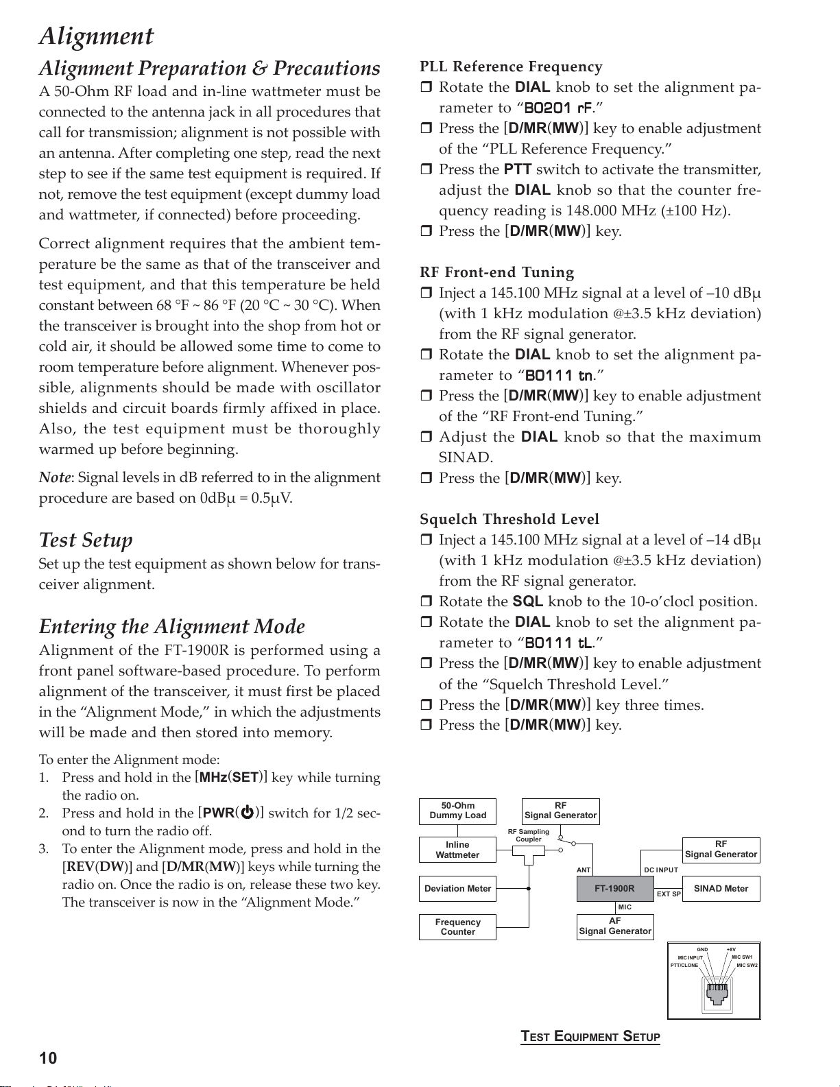
FT-1900R
Inline
Watt met er
SINAD MeterDeviation Meter
Frequency
Counter
RF
Signal Generator
AF
Signal Generator
RF
Signal Generator
50-Ohm
Dummy Load
MIC
ANT
EXT SP
RF Sampling
Coupler
DC INPUT
Alignment Preparation & Precautions
A 50-Ohm RF load and in-line wattmeter must be
connected to the antenna jack in all procedures that
call for transmission; alignment is not possible with
an antenna. After completing one step, read the next
step to see if the same test equipment is required. If
not, remove the test equipment (except dummy load
and wattmeter, if connected) before proceeding.
Correct alignment requires that the ambient tem-
perature be the same as that of the transceiver and
test equipment, and that this temperature be held
constant between 68 °F ~ 86 °F (20 °C ~ 30 °C). When
the transceiver is brought into the shop from hot or
cold air, it should be allowed some time to come to
room temperature before alignment. Whenever pos-
sible, alignments should be made with oscillator
shields and circuit boards firmly affixed in place.
Also, the test equipment must be thoroughly
warmed up before beginning.
Note: Signal levels in dB referred to in the alignment
procedure are based on 0dBµ = 0.5µV.
Test Setup
Set up the test equipment as shown below for trans-
ceiver alignment.
Entering the Alignment Mode
Alignment of the FT-1900R is performed using a
front panel software-based procedure. To perform
alignment of the transceiver, it must first be placed
in the “Alignment Mode,” in which the adjustments
will be made and then stored into memory.
To enter the Alignment mode:
1. Press and hold in the
[
MHz
(
SET
)]
key while turning
the radio on.
2. Press and hold in the
[
PWR
( )]
switch for 1/2 sec-
ond to turn the radio off.
3. To enter the Alignment mode, press and hold in the
[REV(DW)] and [D/MR(MW)] keys while turning the
radio on. Once the radio is on, release these two key.
The transceiver is now in the “Alignment Mode.”
PLL Reference Frequency
Rotate the DIAL knob to set the alignment pa-
rameter to “
B0201 rFB0201 rF
B0201 rFB0201 rF
B0201 rF.”
Press the
[
D/MR
(
MW
)]
key to enable adjustment
of the “PLL Reference Frequency.”
Press the PTT switch to activate the transmitter,
adjust the DIAL knob so that the counter fre-
quency reading is 148.000 MHz (±100 Hz).
Press the
[
D/MR
(
MW
)]
key.
RF Front-end Tuning
Inject a 145.100 MHz signal at a level of –10 dBµ
(with 1 kHz modulation @±3.5 kHz deviation)
from the RF signal generator.
Rotate the DIAL knob to set the alignment pa-
rameter to “
B0111 tnB0111 tn
B0111 tnB0111 tn
B0111 tn.”
Press the
[
D/MR
(
MW
)]
key to enable adjustment
of the “RF Front-end Tuning.”
Adjust the DIAL knob so that the maximum
SINAD.
Press the
[
D/MR
(
MW
)]
key.
Squelch Threshold Level
Inject a 145.100 MHz signal at a level of –14 dBµ
(with 1 kHz modulation @±3.5 kHz deviation)
from the RF signal generator.
Rotate the SQL knob to the 10-o’clocl position.
Rotate the DIAL knob to set the alignment pa-
rameter to “
B0111 tLB0111 tL
B0111 tLB0111 tL
B0111 tL.”
Press the
[
D/MR
(
MW
)]
key to enable adjustment
of the “Squelch Threshold Level.”
Press the
[
D/MR
(
MW
)]
key three times.
Press the
[
D/MR
(
MW
)]
key.
Alignment
TEST EQUIPMENT SETUP
MIC SW2
MIC SW1
GND +8V
MIC INPUT
PTT/CLONE
11
S-meter Level (S-1)
Inject a 145.100 MHz signal at a level of –5 dBµ
(with 1 kHz modulation @±3.5 kHz deviation)
from the RF signal generator.
Rotate the DIAL knob to set the alignment pa-
rameter to “
B0111 S1B0111 S1
B0111 S1B0111 S1
B0111 S1.”
Press the
[
D/MR
(
MW
)]
key to enable adjustment
of the “S-meter Level (S-1).”
Press the
[
D/MR
(
MW
)]
key three times.
Press the
[
D/MR
(
MW
)]
key.
S-meter Level (S-9)
Inject a 145.100 MHz signal at a level of +20 dBµ
(with 1 kHz modulation @±3.5 kHz deviation)
from the RF signal generator.
Rotate the DIAL knob to set the alignment pa-
rameter to “
B0111 S9B0111 S9
B0111 S9B0111 S9
B0111 S9.”
Press the
[
D/MR
(
MW
)]
key to enable adjustment
of the “S-meter Level (S-9).”
Press the
[
D/MR
(
MW
)]
key three times.
Press the
[
D/MR
(
MW
)]
key.
TX Power (High)
Rotate the DIAL knob to set the alignment pa-
rameter to “
B0101 HPB0101 HP
B0101 HPB0101 HP
B0101 HP.”
Press the
[
D/MR
(
MW
)]
key to enable adjustment
of the “TX Power (High).”
Press the PTT switch to activate the transmitter,
adjust the DIAL knob so that the RF Power Meter
reading is 50 W (±2.0W).
Press the
[
D/MR
(
MW
)]
key.
TX Power (Low 3)
Rotate the DIAL knob to set the alignment pa-
rameter to “
B0101 L3B0101 L3
B0101 L3B0101 L3
B0101 L3.”
Press the
[
D/MR
(
MW
)]
key to enable adjustment
of the “TX Power (Low 3).”
Press the PTT switch to activate the transmitter,
adjust the DIAL knob so that the RF Power Meter
reading is 25 W (±1.5 W).
Press the
[
D/MR
(
MW
)]
key.
TX Power (Low 2)
Rotate the DIAL knob to set the alignment pa-
rameter to “
B0101 L2B0101 L2
B0101 L2B0101 L2
B0101 L2.”
Press the
[
D/MR
(
MW
)]
key to enable adjustment
of the “TX Power (Low 2).”
Press the PTT switch to activate the transmitter,
adjust the DIAL knob so that the RF Power Meter
reading is 10 W (±1.0 W).
Press the
[
D/MR
(
MW
)]
key.
TX Power (Low 1)
Rotate the DIAL knob to set the alignment pa-
rameter to “
B0101 L1B0101 L1
B0101 L1B0101 L1
B0101 L1
.”
Press the
[
D/MR
(
MW
)]
key to enable adjustment
of the “TX Power (Low 1).”
Press the PTT switch to activate the transmitter,
adjust the DIAL knob so that the RF Power Meter
reading is 5 W (±0.5 W).
Press the
[
D/MR
(
MW
)]
key.
TX Deviation
Inject a 1 kHz, 50 mV signal from the Audio Gen-
erator.
Rotate the DIAL knob to set the alignment pa-
rameter to “
B0101 dUB0101 dU
B0101 dUB0101 dU
B0101 dU.”
Press the
[
D/MR
(
MW
)]
key to enable adjustment
of the “TX Deviation.”
Press the PTT switch to activate the transmitter,
adjust the DIAL knob so that the Deviation Meter
reading is 4.2 kHz (±0.1 kHz) (EXP version: 4.5
kHz ± 0.1 kHz).
Press the
[
D/MR
(
MW
)]
key.
CTCSS TX Deviation
Rotate the DIAL knob to set the alignment pa-
rameter to “
B0101 100B0101 100
B0101 100B0101 100
B0101 100.”
Press the
[
D/MR
(
MW
)]
key to enable adjustment
of the “CTCSS TX Deviation.”
Press the PTT switch to activate the transmitter,
adjust the DIAL knob so that the Deviation Meter
reading is 0.6 kHz (±0.05 kHz).
Press the
[
D/MR
(
MW
)]
key.
Alignment
Loading...