

UC1872
UC2872
UC3872
07/99
FEATURES
•
Controls Different Types of Lamps:
Cold Cathode Fluorescent, Neon, and
Gas Discharge
•
Zero Voltage Switching (ZVS) of
Push-Pull Drivers
•
Accurate Control of Lamp Current
•
Variable Lamp Intensity Control
•
1µA Disable Current
•
4.5V to 24V Operation
•
Open Lamp Detection Circuitry
DESCRIPTION
The UC3872 is a resonant lamp ballast controller optimized for driving
cold cathode fluorescent, neon, and other gas discharge lamps. The res
-
onant power stage develops a sinusoidal lamp drive voltage, and mini
mizes switching loss and EMI generation. Lamp intensity adjustment is
accomplished with a buck regulator, which is synchronized to the external
power stage’s resonant frequency. Suitable for automotive and battery
powered applications, the UC3872 draws only 1µA when disabled.
Soft start and open lamp detect circuitry have been incorporated to mini
mize component stresses. Open lamp detection is enabled at the comple
tion of a soft start cycle. The chip is optimized for smooth duty cycle
control to 100%.
Other features include a precision 1.2% reference, undervoltage lockout,
and accurate minimum and maximum frequency control.
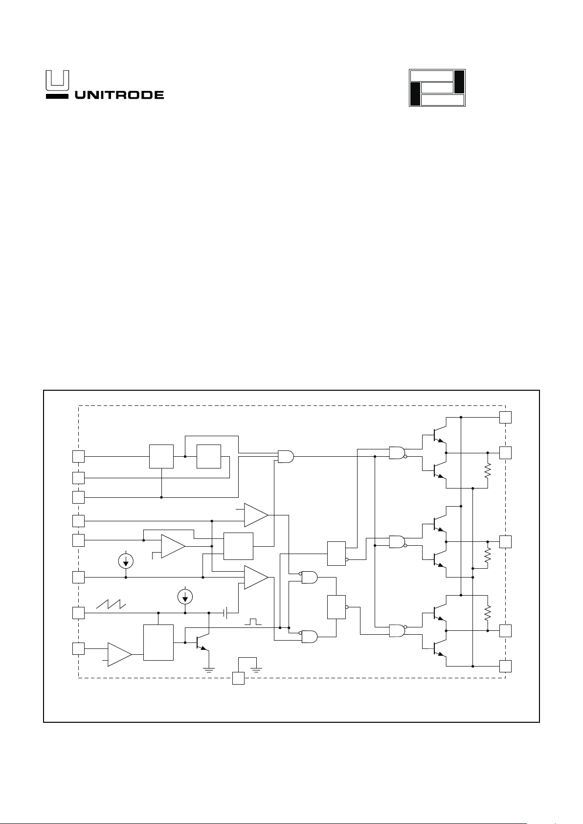
Resonant Lamp Ballast Controller
4
6
5
3
2
12
13
1
14
7
8
+
–
0.5V
SYNC
OUT
SENSE
OSCILLATOR
GND
+
–
–
+
OPEN
LAMP
DETECT
+
–
+
–
UVLO
3.0V
REF
10
9
11
R
S
T
TOGGLE
50k
50k
50k
PUSH PULL
OUTPUTS
N-CHANNEL
VC
AOUT
BOUT
COUT
PGND
0.1V
PWM
1
0.2V
200µA
ZERO DETECT
ZD
CT
SS
INV
COMP
ENBL
REF
VCC
1.5V
20µA
(HIGH=ENABLE)
BUCK DRIVE
P-CHANNEL
EA
BLOCK DIAGRAM
UDG-99112
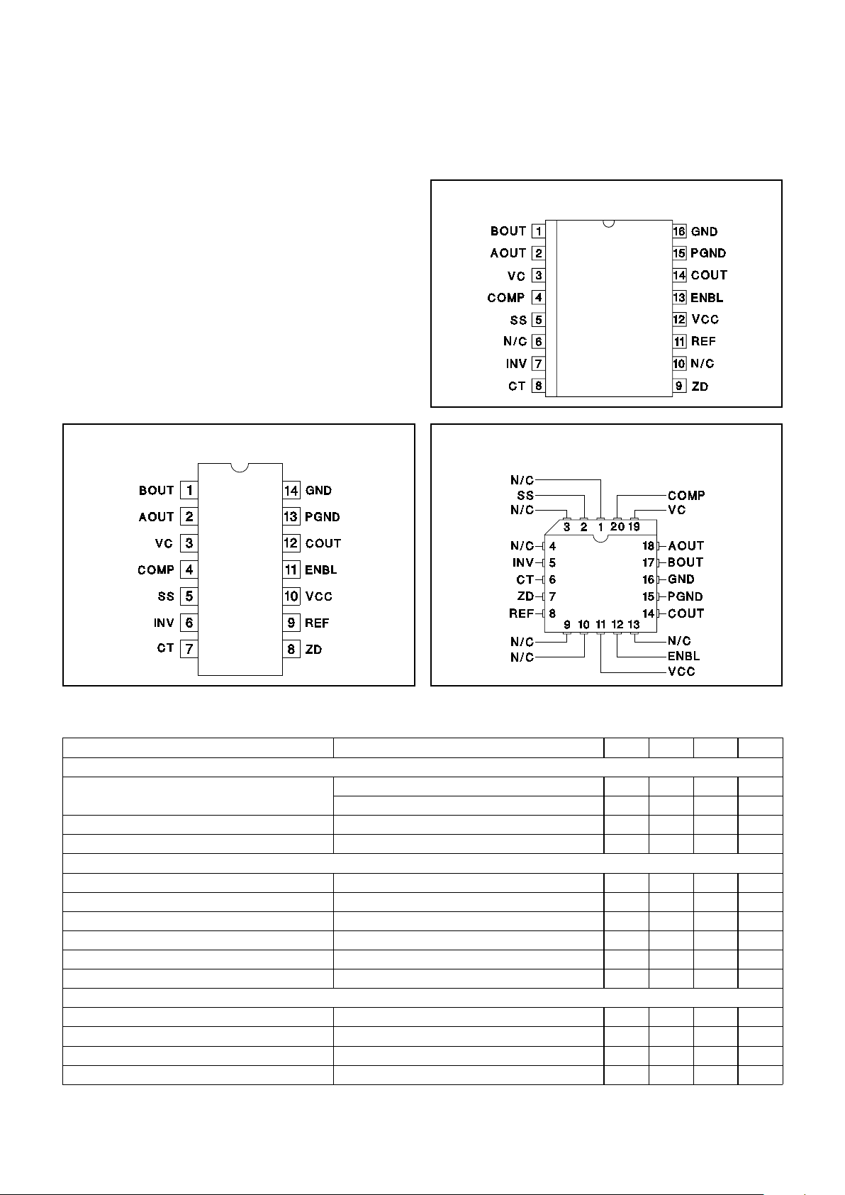
Note: Pin numbers shown are for DIP package.
application
INFO
available
2
UC1872
UC2872
UC3872
ELECTRICAL CHARACTERISTICS:
Unless otherwise stated, these parameters apply for TJ = −55°C to +125°C for the
UC1872, –40°C to +85°C for the UC2872, −0°C to +70°C for the UC3872; VCC= 5V, VC = 15V, V
ENBL
= 5V, CT = 1nF, ZD = 1V.
PARAMETER TEST CONDITIONS MIN TYP MAX UNITS
Reference Section
Output Voltage T
J = 25°C 2.963 3.000 3.037 V
Over Temperature 2.940 3.000 3.060 V
Line Regulation VCC = 4.75V to 18V 10 mV
Load Regulation I
O
= 0 to −5mA 10 mV
Oscillator Section
Free Running Frequency T
J
= 25°C 576878kHz
Maximum Synchronization Frequency T
J
= 25°C 160 200 240 kHz
Charge Current V
CT
= 1.5V 180 200 220 µA
Voltage Stability 2%
Temperature Stability 48%
Zero Detect Threshold 0.46 0.5 0.56 V
Error Amp Section
Input Voltage V
O
= 2V 1.445 1.475 1.505 V
Input Bias Current −0.4 −2 µA
Open Loop Gain V
O
= 0.5 to 3V 65 90 dB
Output High V
INV
= 1.3V 3.1 3.5 3.9 V
ABSOLUTE MAXIMUM RATINGS
Analog Inputs . . . . . . . . . . . . . . . . . . . . . . . . . . . . . −0.3 to +10V
VCC, VC Voltage. . . . . . . . . . . . . . . . . . . . . . . . . . . . . . . . +24V
ZD Input Current
High Impedance Source . . . . . . . . . . . . . . . . . . . . . . +10mA
ZD Input Voltage
Low Impedance Source . . . . . . . . . . . . . . . . . . . . . . . . +24V
Power Dissipation at T
A = 25°C . . . . . . . . . . . . . . . . . . . . . . 1W
Storage Temperature . . . . . . . . . . . . . . . . . . . −65°C to +150°C
Lead Temperature. . . . . . . . . . . . . . . . . . . . . . . . . . . . . . 300°C
Note 1: Currents are positive into, negative out of the specified
terminal.
Note 2: Consult Packaging Section of Databook for thermal limi
-
tations and considerations of package.
DIL-14 (TOP VIEW)
N Package
PLCC-20 (Top View)
Q Package
CONNECTION DIAGRAMS
SOIC-16, SSOP-16 (TOP VIEW)
DW, M Package
3
UC1872
UC2872
UC3872
ELECTRICAL CHARACTERISTICS:
Unless otherwise stated, these parameters apply for TJ = −55°C to +125°C for the
UC1872, –40°C to +85°C for the UC2872, −0°C to +70°C for the UC3872; VCC= 5V, VC = 15V, V
ENBL
= 5V, CT = 1nF, ZD = 1V.
PARAMETER TEST CONDITIONS MIN TYP MAX UNITS
Error Amp Section (cont.)
Output Low V
INV
= 1.7V 0.1 0.2 V
Output Source Current V
INV
= 1.3V, VO= 2V –350 –500 µA
Output Sink Current V
INV
= 1.7V, VO= 2V 10 20 mA
Common Mode Range 0V
IN
-1V V
Unity Gain Bandwidth T
J
= 25°C (Note 4) 1 MHz
Open Lamp Detect Section
Soft Start Threshold V
INV
= 0V 2.9 3.4 3.8 V
Open Lamp Detect Threshold V
SS
= 4.2V 0.6 1.0 1.4 V
Soft Start Current V
SS
= 2V 10 20 40 µA
Output Section
Output Low Level I
OUT
= 0, Outputs A and B 0.05 0.2 V
I
OUT
= 10mA 0.1 0.4 V
I
OUT
= 100mA 1.5 2.2 V
Output High Level I
OUT
= 0, Output C 13.9 14.9 V
I
OUT
= −10mA 13.5 14.3 V
I
OUT
= −100mA 12.5 13.5 V
Rise Time T
J
= 25°C, Cl = 1nF (Note 4) 30 80 ns
Fall Time T
J
= 25°C, Cl = 1nF (Note 4) 30 80 ns
Output Dynamics
Out A and B Duty Cycle 48 49.9 50 %
Out C Max Duty Cycle V
INV
= 1V 100 %
Out C Min Duty Cycle V
INV
= 2V 0 %
Under Voltage Lockout Section
Startup Threshold Voltage 3.7 4.2 4.5 V
Hysteresis 120 200 280 mV
Enable Section
Input High Threshold 2V
Input Low Threshold 0.8 V
Input Current V
ENBL
= 5V 150 400 µA
Supply Current Section
VCC Supply Current VCC = 24V 6 14 mA
VC Supply Current VC = 24V 5 12 mA
ICC Disabled VCC = 24V, V
ENBL = 0V 1 10 µA
Note 3: Unless otherwise specified, all voltages are with respect to ground. Currents are positive into, and negative out of the
specified terminal.
Note 4: Guaranteed by design. Not 100% tested in production.

4
UC1872
UC2872
UC3872
AOUT, BOUT: These outputs provide complementary
drive signals for the push-pull N-channel MOSFETs.
Each one is high for 50% of the time, switching states
each time a zero-detect is sensed.
COMP: COMP is the output terminal of the error ampli
fier. Compensation components are normally connected
between COMP and INV. Connecting a capacitor from
this pin to ground limits turn on current and blanks the
open lamp detect signal allowing the lamp to start.
COUT: This output directly drives the bulk regulator
P-channel MOSFET. COUT turn-on is synchronized to
each zero-detect, and therefore switches at twice the fre
quency of AOUT and BOUT. The modulator controlling
COUT is designed to provide smooth control up to 100%
duty cycle.
CT: A capacitor connected between this pin and GND
ground sets the synchronization frequency range. The
capacitor is charged with approximately 200µA, creating
a linear ramp which is used by COUT’s (buck regulator
driver) PWM comparator.
ENBL: When ENBL is driven high the device is enabled.
When ENBL is pulled low, the IC is shut down and typically draws 1µA.
GND: This pin is the ground reference point for the internal reference and all thresholds.
INV: This pin is the inverting input to the error amplifier
and the input for the open lamp detect circuitry. If the
voltage at INV is below the 1V open lamp detect thresh
-
old, the outputs are disabled.
PGND: This pin is the high current ground connection for
the three output drivers.
REF: This pin is connected to the 3V reference voltage
which is used for the internal logic. Bypass REF to
ground with a 0.01µF ceramic capacitor for proper opera
-
tion.
VC: VC is the power supply voltage connection for the
output drivers. Bypass it to ground with a 0.1µF ceramic
capacitor for proper operation.
VCC: VCC is the positive supply voltage for the chip. Its
operating range is from 4.2V to 24V. Bypass VCC to
ground with a 0.1µF ceramic capacitor for proper opera
-
tion.
ZD: The zero-detect input senses when the trans-
former’s primary center tap voltage falls to zero to synchronize the sawtooth voltage waveform on CT. The
threshold is approximately 0.5V, providing a small
amount of offset such that with propagation delay,
zero-volt switching occurs. A resistor (typically 10k)
should be connected between ZD and the primary center tap to limit input current at turn off.
PIN DESCRIPTIONS
Figure 1 shows a complete application circuit using the
UC3872 Resonant Lamp Ballast Controller. The IC pro
vides all drive, control and housekeeping functions. The
buck output voltage (transformer center-tap) provides the
zero crossing and synchronization signals.
The buck modulator drives a P-channel MOSFET di
rectly, and operates over a 0-100% duty-cycle range.
The modulation range includes 100%, allowing operation
with minimal headroom.
The oscillator and synchronization circuitry are shown in
Figure 2. The oscillator is designed to synchronize over a
3:1 frequency range. In an actual application however,
the frequency range is only about 1.5:1. A zero detect
comparator senses the primary center-tap voltage, gen
erating a synchronization pulse when the resonant wave
-
form falls to zero. The actual threshold is 0.5 volts,
providing a small amount of anticipation to offset propa
-
gation delay.
The synchronization pulse width is the time required for
the 4mA current sink to discharge the timing capacitor to
0.1 volts. This pulse width limits the minimum linear con
trol range of the buck regulator. The 200µA current
source charges the capacitor to a maximum of 3 volts. A
comparator blanks the zero detect signal until the capac
itor voltage exceeds 1 volt, preventing multiple synchro
nization pulse generation and setting the maximum
frequency. If the capacitor voltage reaches 3 volts (a zero
detection has not occurred) an internal clock pulse is
generated to limit the minimum frequency.
APPLICATION INFORMATION

5
UC1872
UC2872
UC3872
Figure 1. Typical application.
UDG-93018-2
A unique protection feature incorporated in the UC3872
is the Open Lamp Detect circuit. An open lamp interrupts
the current feedback loop and causes very high second
-
ary voltage. Operation in this mode will usually break
down the transformer’s insulation, causing permanent
damage to the converter. The open lamp detect circuit,
shown in Figure 3 senses the lamp current feedback sig
nal at the error amplifier’s input, and shuts down the out
puts if insufficient signal is present. Soft start circuitry
limits initial turn-on currents and blanks the open lamp
detect signal.
Other features are included to minimize external circuitry
requirements. A logic level enable pin shuts down the IC,
allowing direct connection to a battery. During shutdown, the IC typically draws less than 1µA. The UC3872,
operating from 4.5V to 24V, is compatible with almost all
battery voltages used in portable computers and auto
-
motive applications. Undervoltage lockout circuitry dis
ables operation until sufficient supply voltage is
available, and a 1% voltage reference insures accurate
operation.
APPLICATION INFORMATION (cont.)

6
UC1872
UC2872
UC3872
APPLICATIONS INFORMATION
7
8
+
–
+
–
200µA
+
–
+
–
CT
0.1V
3.0V
MAX FREQ
COMPARATOR
0.5V
ZD
1.0V
ZERO DETECT
CLK
S
Q
R
4mA
DISCHARGE
COMPARATOR
MIN FREQ
COMPARATOR
Figure 2. UC3872 oscillator section.
Figure 3. UC3872 open lamp detect circuitry.
UNITRODE CORPORATION
7 CONTINENTAL BLVD. • MERRIMACK, NH 03054
TEL. (603) 424-2410 FAX (603) 424-3460
UDG-99005

IMPORTANT NOTICE
T exas Instruments and its subsidiaries (TI) reserve the right to make changes to their products or to discontinue
any product or service without notice, and advise customers to obtain the latest version of relevant information
to verify, before placing orders, that information being relied on is current and complete. All products are sold
subject to the terms and conditions of sale supplied at the time of order acknowledgement, including those
pertaining to warranty, patent infringement, and limitation of liability.
TI warrants performance of its semiconductor products to the specifications applicable at the time of sale in
accordance with TI’s standard warranty. Testing and other quality control techniques are utilized to the extent
TI deems necessary to support this warranty. Specific testing of all parameters of each device is not necessarily
performed, except those mandated by government requirements.
CERT AIN APPLICATIONS USING SEMICONDUCTOR PRODUCTS MAY INVOLVE POTENTIAL RISKS OF
DEATH, PERSONAL INJURY, OR SEVERE PROPERTY OR ENVIRONMENTAL DAMAGE (“CRITICAL
APPLICATIONS”). TI SEMICONDUCTOR PRODUCTS ARE NOT DESIGNED, AUTHORIZED, OR
WARRANTED TO BE SUITABLE FOR USE IN LIFE-SUPPORT DEVICES OR SYSTEMS OR OTHER
CRITICAL APPLICATIONS. INCLUSION OF TI PRODUCTS IN SUCH APPLICA TIONS IS UNDERSTOOD T O
BE FULLY AT THE CUSTOMER’S RISK.
In order to minimize risks associated with the customer’s applications, adequate design and operating
safeguards must be provided by the customer to minimize inherent or procedural hazards.
TI assumes no liability for applications assistance or customer product design. TI does not warrant or represent
that any license, either express or implied, is granted under any patent right, copyright, mask work right, or other
intellectual property right of TI covering or relating to any combination, machine, or process in which such
semiconductor products or services might be or are used. TI’s publication of information regarding any third
party’s products or services does not constitute TI’s approval, warranty or endorsement thereof.
Copyright 1999, Texas Instruments Incorporated
 Loading...