Telefunken TSDF1205W, TSDF1205RW, TSDF1205R, TSDF1205 Datasheet

TSDF1205/TSDF1205R/TSDF1205W/TSDF1205RW
Vishay Telefunken
Silicon NPN Planar RF Transistor
Electrostatic sensitive device.
Observe precautions for handling.
Applications
For low noise and small signal low power amplifiers. This transistor has superior noise figure and associated gain performance at UHF, VHF and microwave frequencies.
Features
DLow power applications
DVery low noise figure
DHigh transition frequency fT = 12 GHz
2 |
1 |
1 |
2 |
|
94 9279 |
13 579 |
|
94 9278 |
95 10831 |
3 |
|
4 |
4 |
|
3 |
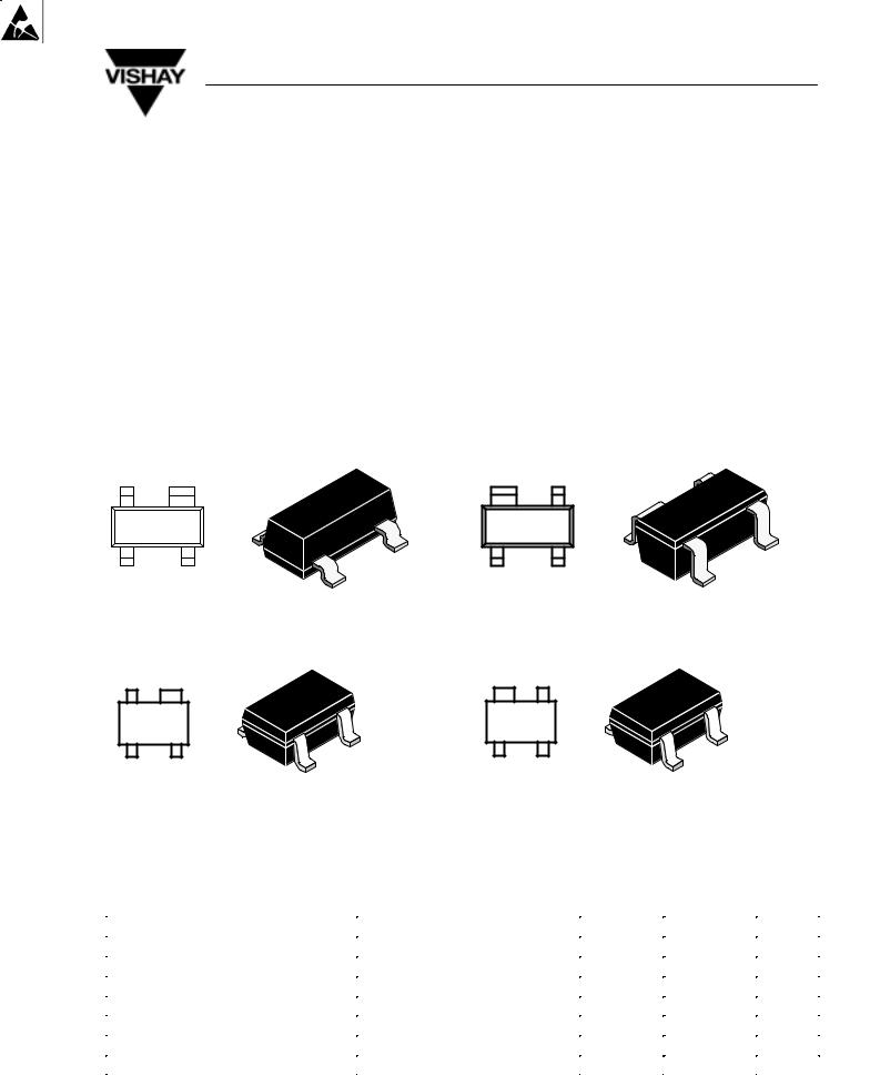
TSDF1205 Marking: F05 |
TSDF1205R Marking: 05F |
||||
Plastic case (SOT 143) |
Plastic case (SOT 143R) |
||||
1 = Collector, 2 = Emitter, 3 = Base, 4 = Emitter |
1 = Collector, 2 = Emitter, 3 = Base, 4 = Emitter |
||||
2 |
1 |
|
1 |
2 |
|
|
13 653 |
13 566 |
|
13 654 |
13 566 |
3 |
4 |
|
4 |
3 |
|
TSDF1205W Marking: WF0 |
|
TSDF1205RW Marking: W0F |
|
||
Plastic case (SOT 343) |
|
Plastic case (SOT 343R) |
|
||
1 = Collector, 2 = Emitter, 3 = Base, 4 = Emitter |
1 = Collector, 2 = Emitter, 3 = Base, 4 = Emitter |
||||
Absolute Maximum Ratings
Tamb = 25_C, unless otherwise specified
Parameter |
Test Conditions |
Symbol |
Value |
Unit |
Collector-base voltage |
|
VCBO |
9 |
V |
Collector-emitter voltage |
|
VCEO |
4 |
V |
Emitter-base voltage |
|
VEBO |
2 |
V |
Collector current |
|
IC |
12 |
mA |
Total power dissipation |
Tamb ≤ 132 °C |
Ptot |
40 |
mW |
Junction temperature |
|
Tj |
150 |
°C |
Storage temperature range |
|
Tstg |
±65 to +150 |
°C |
|
|
|
|
|
Document Number 85065 |
|
www.vishay.de •FaxBack +1-408-970-5600 |
||
Rev. 5, 30-Jun-00 |
|
|
|
1 (6) |

TSDF1205/TSDF1205R/TSDF1205W/TSDF1205RW
Vishay Telefunken
Maximum Thermal Resistance
Tamb = 25_C, unless otherwise specified
Parameter |
Test Conditions |
Symbol |
Value |
Unit |
Junction ambient |
on glass fibre printed board (25 x 20 x 1.5) mm3 |
R |
450 |
K/W |
|
plated with 35mm Cu |
thJA |
|
|
|
|
|
|
Electrical DC Characteristics
Tamb = 25_C, unless otherwise specified
Parameter |
Test Conditions |
Symbol |
Min |
Typ |
Max |
Unit |
Collector cut-off current |
VCE = 12 V, VBE = 0 |
ICES |
|
|
100 |
mA |
Collector-base cut-off current |
VCB = 10 V, IE = 0 |
ICBO |
|
|
100 |
nA |
Emitter-base cut-off current |
VEB = 1 V, IC = 0 |
IEBO |
|
|
2 |
mA |
Collector-emitter breakdown voltage |
IC = 1 mA, IB = 0 |
V(BR)CEO |
4 |
|
|
V |
Collector-emitter saturation voltage |
IC = 5 mA, IB = 0.5 mA |
VCEsat |
|
0.1 |
0.5 |
V |
DC forward current transfer ratio |
VCE = 2 V, IC = 2 mA |
hFE |
50 |
120 |
250 |
|
Electrical AC Characteristics
Tamb = 25_C, unless otherwise specified
Parameter |
|
Test Conditions |
Symbol |
Min |
Typ |
Max |
Unit |
|||||
Transition frequency |
VCE = 2 |
V, IC = |
5 mA, f = 1 GHz |
fT |
|
12 |
|
GHz |
||||
Collector-base capacitance |
VCB = 1 |
V, f = 1 MHz |
|
|
Ccb |
|
0.2 |
|
pF |
|||
Collector-emitter capacitance |
VCE = 1 |
V, f = 1 MHz |
|
|
Cce |
|
0.35 |
|
pF |
|||
Emitter-base capacitance |
VEB = 0.5 V, f = 1 MHz |
|
|
Ceb |
|
0.15 |
|
pF |
||||
Noise figure |
VCE = 2 |
V, IC = |
2 mA, ZS = ZSopt, |
F |
|
1.3 |
|
dB |
||||
|
ZL = 50 W, f = 2 GHz |
|
|
|
|
|
|
|
||||
Power gain |
VCE = 2 |
V, IC = |
2 mA, |
|
|
Gpe |
|
13 |
|
dB |
||
|
f = 2 GHz (@Fopt) |
|
|
|
|
|
|
|
||||
|
VCE = 2 |
V, IC = |
5 mA, ZS = ZSopt, |
Gpe |
|
11.5 |
|
dB |
||||
|
ZL = 50 W f = 2 GHz |
|
|
|
|
|
|
|
||||
Transducer gain |
V = 2 |
V, I |
C |
= |
5 mA, Z |
0 |
= 50 W, |
S 2 |
|
12.5 |
|
dB |
|
CE |
|
|
|
|
21e |
|
|
|
|
||
|
f = 2 GHz |
|
|
|
|
|
|
|
|
|
|
|
www.vishay.de •FaxBack +1-408-970-5600 |
Document Number 85065 |
2 (6) |
Rev. 5, 30-Jun-00 |
 Loading...