


TSOP1538SD1
Telefunken TSOP1538SD1, TSOP1537SD1, TSOP1530SD1, TSOP1536SD1, TSOP1533SD1 Datasheet
...
TSOP15..SD1
Vishay Telefunken
1 (7)Rev. 7, 30-Mar-01
www.vishay.com
Document Number 82071
Photo Modules for PCM Remote Control Systems
Available types for different carrier frequencies
Type fo Type fo
TSOP1530SD1 30 kHz TSOP1533SD1 33 kHz
TSOP1536SD1 36 kHz TSOP1537SD1 36.7 kHz
TSOP1538SD1 38 kHz TSOP1540SD1 40 kHz
TSOP1556SD1 56 kHz
Description
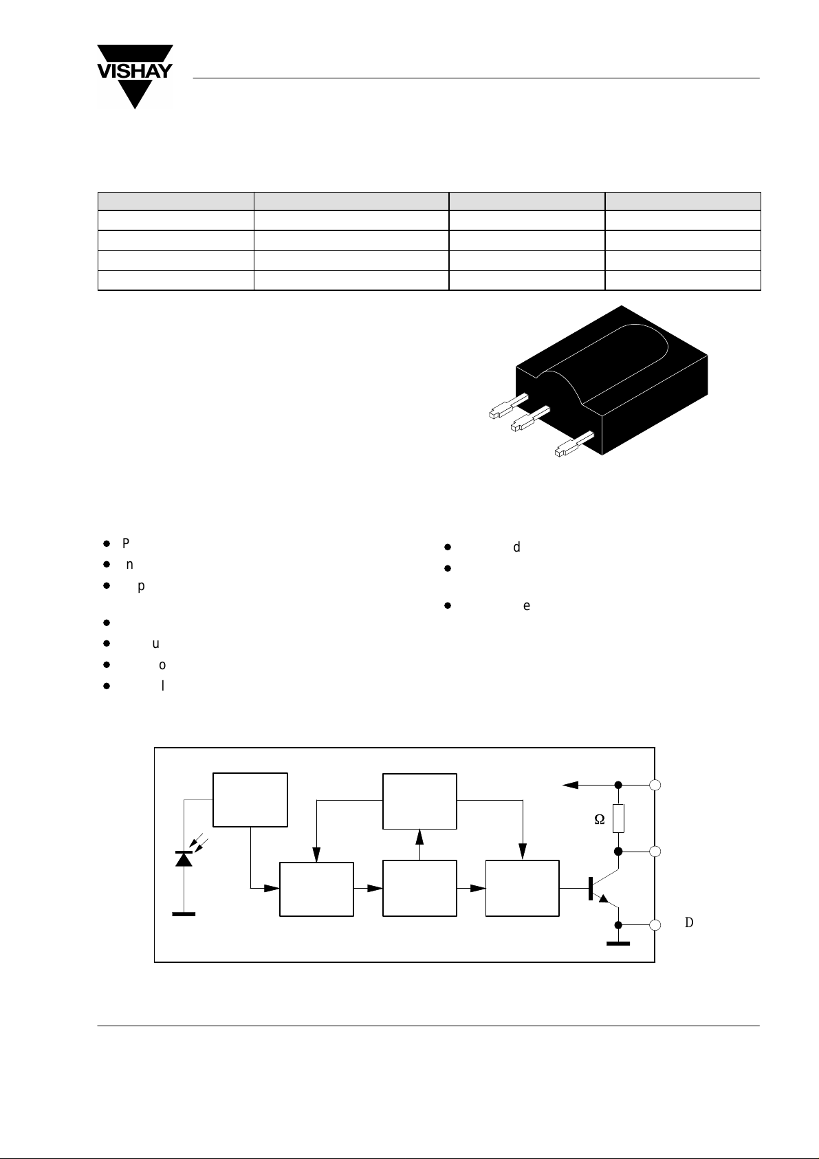
The TSOP15..SD1 – series are miniaturized receivers
for infrared remote control systems. PIN diode and
preamplifier are assembled on lead frame, the epoxy
package is designed as IR filter.
The demodulated output signal can directly be
decoded by a microprocessor. The main benefit is the
reliable function even in disturbed ambient and the
protection against uncontrolled output pulses.
13 645
Features
D
Photo detector and preamplifier in one package
D
Internal filter for PCM frequency
D
Improved shielding against electrical field
disturbance
D
TTL and CMOS compatibility
D
Output active low
D
Low power consumption
D
Suitable burst length ≥10 cycles/burst
Special Features
D
Improved directivity
D
Enhanced immunity against all kinds of
disturbance light
D
No occurrence of disturbance pulses at the
output
Block Diagram
94 8136
PIN
Input
AGC
Control
Circuit
Band
Pass
Demodu-
lator
80 k
W
1
2
3
V
S
OUT
GND
TSOP15..SD1
Vishay Telefunken
Rev. 7, 30-Mar-01
www.vishay.com
Document Number 82071
2 (7)
Absolute Maximum Ratings
T
amb
= 25
_
C
Parameter Test Conditions Symbol Value Unit
Supply Voltage (Pin 2) V
S
–0.3...6.0 V
Supply Current (Pin 2) I
S
5 mA
Output Voltage (Pin 3) V
O
–0.3...6.0 V
Output Current (Pin 3) I
O
5 mA
Junction Temperature T
j
100
°
C
Storage Temperature Range T
stg
–25...+85
°
C
Operating Temperature Range T
amb
–25...+85
°
C
Power Consumption (T
amb
x
85
°
C) P
tot
50 mW
Soldering Temperature t
x
10 s, 1 mm from case T
sd
260
°
C
Basic Characteristics
T
amb
= 25
_
C
Parameter Test Conditions Symbol Min Typ Max Unit
Supply Current (Pin 2) V
S
= 5 V, E
v
= 0 I
SD
0.4 0.6 1.5 mA
y()
V
S
= 5 V, E
v
= 40 klx, sunlight I
SH
1.0 mA
Supply Voltage (Pin 2) V
S
4.5 5.5 V
Transmission Distance E
v
= 0, test signal see fig.7,
IR diode TSAL6200, I
F
= 300 mA
d 35 m
Output Voltage Low
(Pin 3)
I
OSL
= 0.5 mA,E
e
= 0.7 mW/m
2
,
f = f
o
, t
p
/T = 0.4
V
OSL
250 mV
Irradiance
(30 – 40 kHz)
Pulse width tolerance:
t
pi
– 5/f
o
< t
po
< t
pi
+ 6/f
o
,
test signal see fig.7
E
e
min
0.25 0.38 mW/m
2
Irradiance
(56 kHz)
Pulse width tolerance:
t
pi
– 5/f
o
< t
po
< t
pi
+ 6/f
o
,
test signal see fig.7
E
e
min
0.3 0.45 mW/m
2
Irradiance t
pi
– 5/f
o
< t
po
< t
pi
+ 6/f
o
E
e
max
30 W/m
2
Directivity Angle of half transmission distance ϕ
1/2
±55 deg
Application Circuit
14375
TSAL62..
TSOP15..
2
3
1
4.7
m
F *)
m
C
>10 k
W
optional
100
W
*)
+5V
*) recommended to suppress power supply disturbances
GND
**) The output voltage should not be hold continuously at a voltage below 3.3V by the external circuit.
**)
TSOP15..SD1
Vishay Telefunken
3 (7)Rev. 7, 30-Mar-01
www.vishay.com
Document Number 82071
Suitable Data Format
The circuit of the TSOP15..SD1 is designed in that
way that unexpected output pulses due to noise or
disturbance signals are avoided. A bandpassfilter, an
integrator stage and an automatic gain control are
used to suppress such disturbances.
The distinguishing mark between data signal and
disturbance signal are carrier frequency, burst length
and duty cycle.
The data signal should fullfill the following condition:
• Carrier frequency should be close to center
frequency of the bandpass (e.g. 38kHz).
• Burst length should be 10 cycles/burst or longer.
• After each burst which is between 10 cycles and 70
cycles a gap time of at least 14 cycles is neccessary.
• For each burst which is longer than 1.8ms a
corresponding gap time is necessary at some time in
the data stream. This gap time should be at least 4
times longer than the burst.
• Up to 800 short bursts per second can be received
continuously .
Some examples for suitable data format are:
NEC Code (repetitive pulse), NEC Code (repetitive
data), Toshiba Micom Format, Sharp Code, RC5
Code, RC6 Code, R–2000 Code.
When a disturbance signal is applied to the
TSOP15..SD1 it can still receive the data signal.
However the sensitivity is reduced to that level that no
unexpected pulses will occure.
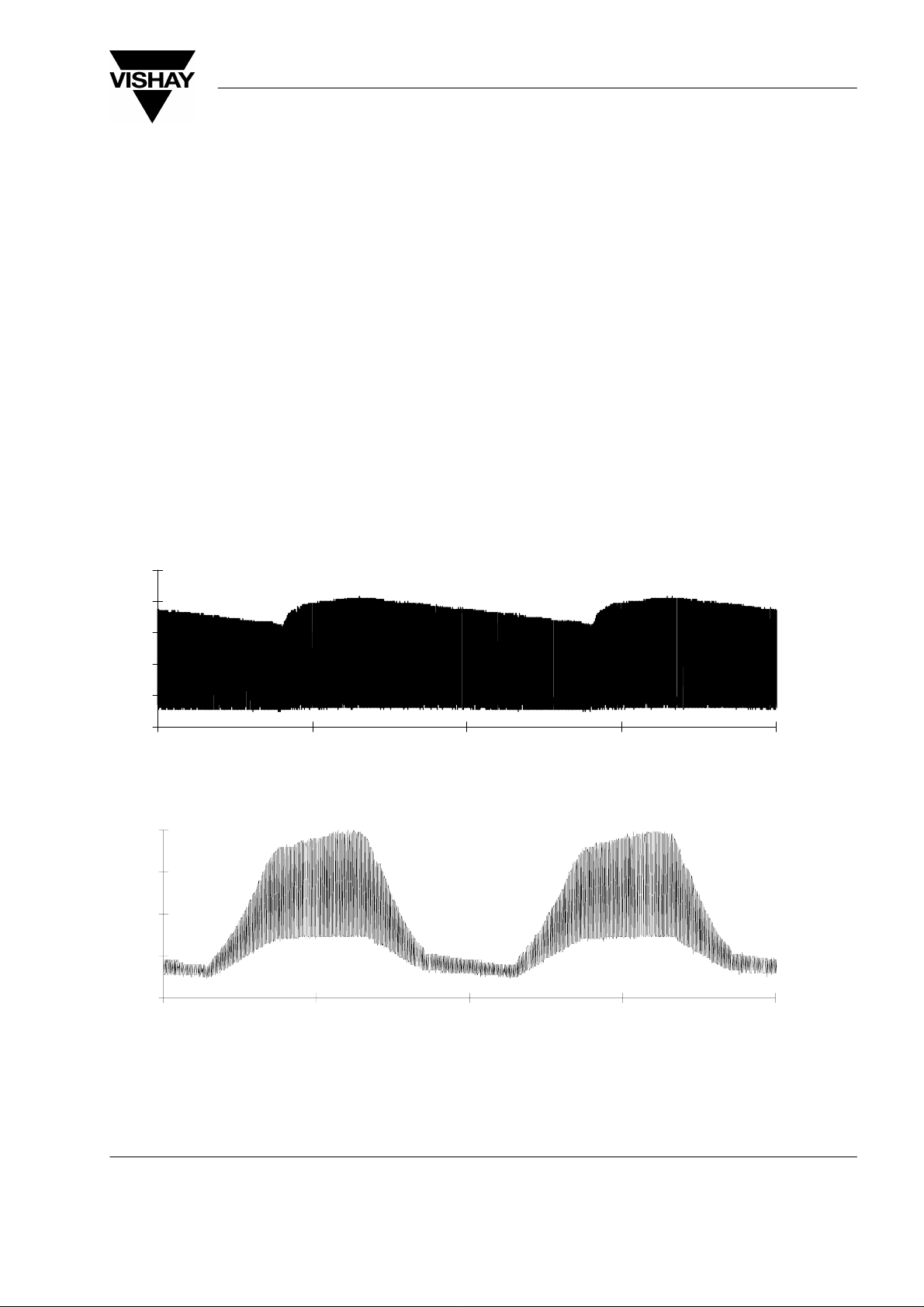
Some examples for such disturbance signals which
are suppressed by the TSOP15..SD1 are:
• DC light (e.g. from tungsten bulb or sunlight)
• Continuous signal at 38kHz or at any other
frequency
• Signals from fluorescent lamps with electronic
ballast with high or low modulation (see Figure A or
Figure B).
0 5 10 15 20
time [ms]
Figure A: IR Signal from Fluorescent Lamp with low Modulation
0 5 10 15 20
time [s]
Figure B: IR Signal from Fluorescent Lamp with high Modulation
 Loading...