

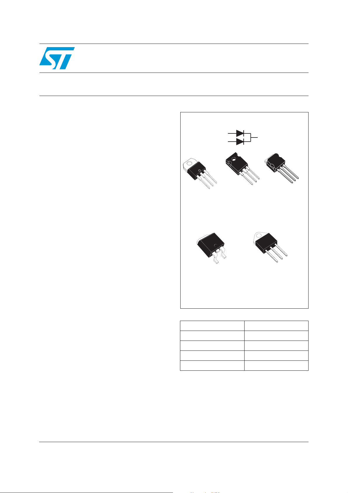
Features
STTH3002C
High efficiency ultrafast diode
■ Suited for SMPS
■ Low losses
■ Low forward and reverse recovery times
■ High surge current capability
■ High junction temperature
■ Insulated version TOP3I:
– Insulated voltage: 2500 V
rms
– Capacitance 12 pF
Description
Dual center tab rectifier suited for switch mode
power supplies and high frequency DC to DC
converters.
Packaged in TO-220AB, TO-247, I
and TOP3I, this device is intended for use in low
voltage, high frequency inverters, free wheeling
and polarity protection
2
PA K , D2PA K ,
K
A1
TO-220AB
STTH3002CT
K
A1
D2PA K
STTH3002CG
A1
A2
A2
STTH3002CW
A2
A1
TO-247
K
A2
K
NC
A1
STTH3002CPI
A2
K
A1
I2PA K
STTH3002CR
A2
K
TOP3I
Table 1. Device summary
I
F(AV)
V
RRM
T
(max) 175 °C
j
VF (typ) 0.75 V
t
(typ) 17 ns
rr
August 2008 Rev 4 1/11
2 x 15A
200 V
www.st.com
Characteristics STTH3002C
1 Characteristics
Table 2. Absolute ratings (limiting values at Tj = 25 °C, unless otherwise specified)
Symbol Parameter Value Unit
V
RRM
I
F(RMS)
I
F(AV)
I
FSM
T
Table 3. Thermal parameters
Repetitive peak reverse voltage 200 V
RMS forward current 50 A
TO-220AB, TO-247,
2
PAK, D2PA K
I
Per diode T
Per device Tc = 145 °C
= 150 °C
c
Average forward current, δ = 0.5
Per diode T
TOP3I
Per device T
= 125 °C
c
= 105 °C
c
Surge non repetitive forward current tp = 10 ms Sinusoidal 180 A
Storage temperature range -65 to +175 °C
stg
T
Maximum operating junction temperature 175 °C
j
15
30
15
30
Symbol Parameter Value Unit
Per diode 1.5
TO-220AB, TO-247, I2PA K , D2PA K
Total 1.0
R
th(j-c)
Junction to case
TOP3I
Per diode 3.5
°C/W
Total 2.3
R
th(c)
Coupling
TOP3I 1.1
TO-220AB, TO-247, I
2
PA K , D2PA K 0 .5
A
When the two diodes 1 and 2 are used simultaneously:
ΔTj(diode 1) = P (diode 1) X R
2/11
(Per diode) + P (diode 2) x R
th(j-c)
th(c)
STTH3002C Characteristics
Table 4. Static electrical characteristics
Symbol Parameter Test conditions Min. Typ Max. Unit
(1)
I
R
V
Reverse leakage current
(2)
Forward voltage drop
F
1. Pulse test: tp = 5 ms, δ < 2 %
2. Pulse test: t
= 380 µs, δ < 2 %
p
= 25 °C
T
j
Tj = 125 °C 10 125
= 25 °C
T
j
V
= V
R
RRM
I
= 15 A 1.05
F
I
= 30 A 1.18
F
IF = 15 A 0.75 0.84
Tj = 150 °C
I
= 30 A
F
20
0.99
To evaluate the conduction losses use the following equation:
P = 0.69 x I
Table 5. Dynamic characteristics
Symbol Parameter
t
rr
I
RM
t
fr
V
FP
Reverse recovery time
Reverse recovery current
Forward recovery time
Forward recovery voltage
Figure 1. Peak current versus duty cycle
(per diode)
F(AV)
+ 0.01 I
F2(RMS)
Test conditions
= 1 A, dIF/dt = 200 A/µs,
I
F
= 30 V, Tj = 25 °C
V
R
IF = 15 A, dIF/dt = 200 A/µs,
V
= 160 V, Tj = 125 °C
R
= 15 A, dIF/dt = 200 A/µs
I
F
= 1.1 x V
V
FR
Fmax
IF = 15 A, dIF/dt = 200 A/µs,
T
= 25 °C
j
Figure 2. Forward voltage drop versus
, Tj = 25 °C
forward current (typical values, per
Min. Typ Max. Unit
17 22 ns
67.8 A
110 ns
2.5 V
diode)
I(A)
M
120
100
80
60
40
20
0
P = 10W
0.0 0.1 0.2 0.3 0.4 0.5 0.6 0.7 0.8 0.9 1.0
P = 30W
P = 15W
δ
I
δ
M
T
=tp/T
tp
I(A)
FM
100
90
80
70
60
50
40
30
20
10
0
0.0 0.2 0.4 0.6 0.8 1.0 1.2 1.4 1.6 1.8
T =150°C
j
V(V)
FM
T =25°C
j
µA
V
3/11
Characteristics STTH3002C
Figure 3. Forward voltage drop versus
forward current (maximum values,
per diode)
I(A)
FM
100
90
80
70
60
50
40
30
20
10
0
0.0 0.2 0.4 0.6 0.8 1.0 1.2 1.4 1.6 1.8 2.0
T =150°C
j
V(V)
FM
T =25°C
j
Figure 5. Junction capacitance versus
reverse applied voltage (typical
values, per diode)
C(pF)
1000
100
V (V)
10
0 50 100 150 200
R
F=1MHz
V =30mV
OSC RMS
T =25°C
j
Figure 7. Reverse recovery time versus
dI
/dt (typical values, per diode)
F
t (ns)
rr
70
I =15A
F
V =160V
R
60
50
40
30
20
10
0
10 100 1000
T =125°C
j
dI /dt(A/µs)
F
T =25°C
j
Figure 4. Relative variation of thermal
impedance junction to case versus
pulse duration
Z/R
th(j-c) th(j-c)
1.0
Single pulse
t(s)
0.1
1.E-03 1.E-02 1.E-01 1.E+00
p
Figure 6. Reverse recovery charges versus
dI
/dt (typical values, per diode)
F
Q (nC)
rr
250
I =15A
F
225
V =160V
R
200
175
150
125
100
75
50
25
0
10 100 1000
T =125°C
j
dI /dt(A/µs)
F
T =25°C
j
Figure 8. Peak reverse recovery current
versus dIF/dt (typical values, per
diode)
I (A)
RM
14
I =15A
F
13
V =160V
R
12
11
10
9
8
7
6
5
4
3
2
1
0
10 100 1000
T =125°C
j
dI /dt(A/µs)
F
T =25°C
j
4/11

STTH3002C Ordering information scheme
Figure 9. Dynamic parameters versus
Figure 10. Thermal resistance junction to
junction temperature
Qrr;I [T ]/Qrr;I [T =125°C]
RM j RM j
1.4
I =15A
F
V =160V
R
1.2
1.0
I
0.8
0.6
0.4
0.2
0.0
25 50 75 100 125 150
RM
Q
rr
T (°C)
j
R (° C/W)
th(j-a)
80
70
60
50
40
30
20
10
0
0 2 4 6 8 10 12 14 16 18 20
2 Ordering information scheme
Figure 11. Ordering information scheme
ambient versus copper surface
under each tab (Epoxy printed
circuit board FR4, e
2
PAK
D
S (cm²)
CU
= 35 µm) for
CU
Ultrafast switching diode
Average forward current
30 = 30 A
Repetitive peak reverse voltage
02 = 200 V
Package
CT = TO-220AB in Tube
CW = TO-247 in Tube
CR = I2PAK in Tube
CG = D2PAK in Tube
CG-TR = D2PAK in Tape and reel
CPI = TOP3 in Tube
STTH 30 02 Cxx
5/11

Package information STTH3002C
3 Package information
● Epoxy meets UL94, V0
● Cooling method: by conduction (C)
● Recommended torque values: TO-220AB 0.4 to 0.6 N·m, TO-247 0.55 N·m (1.0 N·m
maximum), TOP3I 0.9 to 1.2 N·m
In order to meet environmental requirements, ST offers these devices in ECOPACK
packages. These packages have a lead-free second level interconnect. The category of
second level interconnect is marked on the package and on the inner box label, in
compliance with JEDEC Standard JESD97. The maximum ratings related to soldering
conditions are also marked on the inner box label. ECOPACK is an ST trademark.
ECOPACK specifications are available at www.st.com.
Table 6. TO-220AB dimensions
DIMENSIONS
®
Ref.
Millimeters Inches
Min. Typ Max. Min. Typ Max.
A 15.20 15.90 0.598 0.625
a1 3.75 0.147
B
Ø I
L
A
I4
l3
a1
l2
a2
C
b2
a2 13.00 14.00 0.511 0.551
B 10.00 10.40 0.393 0.409
F
b1 0.61 0.88 0.024 0.034
b2 1.23 1.32 0.048 0.051
C 4.40 4.60 0.173 0.181
c2
c1 0.49 0.70 0.019 0.027
c2 2.40 2.72 0.094 0.107
e 2.40 2.70 0.094 0.106
b1
e
M
F 6.20 6.60 0.244 0.259
c1
ØI 3.75 3.85 0.147 0.151
I4 15.80 16.40 16.80 0.622 0.646 0.661
L 2.65 2.95 0.104 0.116
l2 1.14 1.70 0.044 0.066
l3 1.14 1.70 0.044 0.066
6/11
M2.60 0.102

STTH3002C Package information
Table 7. TO-247 dimensions
DIMENSIONS
L3
Ref.
Millimeters Inches
Mi n. Typ Ma x. Min . Typ M ax.
A 4.85 5.15 0.191 0.203
V
D 2.20 2.60 0.086 0.102
E 0.40 0.80 0.015 0.031
V
Dia
F 1.00 1.40 0.039 0.055
F1 3.00 0.118
H
A
F2 2.00 0.078
F3 2.00 2.40 0.078 0.094
L5
L
L2
L4
F2
F4
F3
L1
D
F1
V2
F(x3)
G
F4 3.00 3.40 0.118 0.133
G 10.90 0.429
H 15.45 15.75 0.608 0.620
L 19.85 20.15 0.781 0.793
L1 3.70 4.30 0.145 0.169
L2 18.50 0.728
L3 14.20 14.80 0.559 0.582
EM
L4 34.60 1.362
L5 5.50 0.216
M 2.00 3.00 0.078 0.118
V5° 5°
V2 60° 60°
Dia. 3.55 3.65 0.139 0.143
7/11

Package information STTH3002C
Table 8. I2PAK dimensions
DIMENSIONS
E
c2
L2
D
L1
L
b1
A1
b
e
e1
Table 9. TOP3I dimensions
Ref.
A
Millimeters Inches
Min. Max. Min. Max.
A 4.40 4.60 0.173 0.181
A1 2.40 2.72 0.094 0.107
b 0.61 0.88 0.024 0.035
b1 1.14 1.70 0.044 0.067
c 0.49 0.70 0.019 0.028
c2 1.23 1.32 0.048 0.052
D 8.95 9.35 0.352 0.368
e 2.40 2.70 0.094 0.106
e1 4.95 5.15 0.195 0.203
E 10 10.40 0.394 0.409
c
L 13 14 0.512 0.551
L1 3.50 3.93 0.138 0.155
L2 1.27 1.40 0.050 0.055
DIMENSIONS
Ref.
H
R
ØL
K
G
F
A
A 4.4 4.6 0.173 0.181
B
B 1.45 1.55 0.057 0.061
C 14.35 15.60 0.565 0.614
D 0.5 0.7 0.020 0.028
Millimeters Inches
Min. Max. Min. Max.
E 2.7 2.9 0.106 0.114
F 15.8 16.5 0.622 0.650
P
C
G 20.4 21.1 0.815 0.831
H 15.1 15.5 0.594 0.610
J 5.4 5.65 0.213 0.222
JJ
D
E
K 3.4 3.65 0.134 0.144
ØL 4.08 4.17 0.161 0.164
P 1.20 1.40 0.047 0.055
R 4.60 Typ. 0.181 Typ.
8/11

STTH3002C Package information
Table 10. D
L2
L
L3
2
PAK dimensions
E
A1
B2
B
G
2mm min.
FLAT ZONE
DIMENSIONS
Ref.
Millimeters Inches
Min. Max Min. Max.
A 4.40 4.60 0.173 0.181
A
C2
A1 2.49 2.69 0.098 0.106
A2 0.03 0.23 0.001 0.009
B 0.70 0.93 0.027 0.037
D
B2 1.14 1.70 0.045 0.067
C 0.45 0.60 0.017 0.024
C2 1.23 1.36 0.048 0.054
C
R
D 8.95 9.35 0.352 0.368
E 10.00 10.40 0.393 0.409
A2
G 4.88 5.28 0.192 0.208
L 15.00 15.85 0.590 0.624
V2
L2 1.27 1.40 0.050 0.055
L3 1.40 1.75 0.055 0.069
M 2.40 3.20 0.094 0.126
Figure 12. D2PAK footprint (dimensions in mm)
16.90
10.30
8.90
R 0.40 typ. 0.016 typ.
V2 0° 8° 0° 8°
5.08
1.30
3.70
9/11

Ordering information STTH3002C
4 Ordering information
Table 11. Ordering information
Order code Marking Package Weight Base qty Delivery mode
STTH3002CT STTH3002C TO-220AB 2.23 g 50 Tube
STTH3002CW STTH3002C TO-247 4.46 g 30 Tube
STTH3002CR STTH3002C I2PAK 1.49 g 50 Tube
STTH3002CG STTH3002C D
STTH3002CG-TR STTH3002C D
2
PAK 1.48 g 50 Tube
2
PAK 1.48 g 1000 Tape and reel
STTH3002CPI STTH3002C TOP3I 4.7 g 30 Tube
5 Revision history
Table 12. Document revision history
Date Revision Description of changes
Feb-2004 1 First issue
05-Apr-2006 2 Reformatted to current template. Package TOP3I added.
10-May-2006 3 Replace illustrations for TO-247 and I
2
PAK dimensions.
Reformatted to current standards. Updated ECOPACK
25-Aug-2008 4
statement. Updated torque values and TO-247
dimension illustration in Section 3.
10/11

STTH3002C
Please Read Carefully:
Information in this document is provided solely in connection with ST products. STMicroelectronics NV and its subsidiaries (“ST”) reserve the
right to make changes, corrections, modifications or improvements, to this document, and the products and services described herein at any
time, without notice.
All ST products are sold pursuant to ST’s terms and conditions of sale.
Purchasers are solely responsible for the choice, selection and use of the ST products and services described herein, and ST assumes no
liability whatsoever relating to the choice, selection or use of the ST products and services described herein.
No license, express or implied, by estoppel or otherwise, to any intellectual property rights is granted under this document. If any part of this
document refers to any third party products or services it shall not be deemed a license grant by ST for the use of such third party products
or services, or any intellectual property contained therein or considered as a warranty covering the use in any manner whatsoever of such
third party products or services or any intellectual property contained therein.
UNLESS OTHERWISE SET FORTH IN ST’S TERMS AND CONDITIONS OF SALE ST DISCLAIMS ANY EXPRESS OR IMPLIED
WARRANTY WITH RESPECT TO THE USE AND/OR SALE OF ST PRODUCTS INCLUDING WITHOUT LIMITATION IMPLIED
WARRANTIES OF MERCHANTABILITY, FITNESS FOR A PARTICULAR PURPOSE (AND THEIR EQUIVALENTS UNDER THE LAWS
OF ANY JURISDICTION), OR INFRINGEMENT OF ANY PATENT, COPYRIGHT OR OTHER INTELLECTUAL PROPERTY RIGHT.
UNLESS EXPRESSLY APPROVED IN WRITING BY AN AUTHORIZED ST REPRESENTATIVE, ST PRODUCTS ARE NOT
RECOMMENDED, AUTHORIZED OR WARRANTED FOR USE IN MILITARY, AIR CRAFT, SPACE, LIFE SAVING, OR LIFE SUSTAINING
APPLICATIONS, NOR IN PRODUCTS OR SYSTEMS WHERE FAILURE OR MALFUNCTION MAY RESULT IN PERSONAL INJURY,
DEATH, OR SEVERE PROPERTY OR ENVIRONMENTAL DAMAGE. ST PRODUCTS WHICH ARE NOT SPECIFIED AS "AUTOMOTIVE
GRADE" MAY ONLY BE USED IN AUTOMOTIVE APPLICATIONS AT USER’S OWN RISK.
Resale of ST products with provisions different from the statements and/or technical features set forth in this document shall immediately void
any warranty granted by ST for the ST product or service described herein and shall not create or extend in any manner whatsoever, any
liability of ST.
ST and the ST logo are trademarks or registered trademarks of ST in various countries.
Information in this document supersedes and replaces all information previously supplied.
The ST logo is a registered trademark of STMicroelectronics. All other names are the property of their respective owners.
© 2008 STMicroelectronics - All rights reserved
STMicroelectronics group of companies
Australia - Belgium - Brazil - Canada - China - Czech Republic - Finland - France - Germany - Hong Kong - India - Israel - Italy - Japan -
Malaysia - Malta - Morocco - Singapore - Spain - Sweden - Switzerland - United Kingdom - United States of America
www.st.com
11/11
 Loading...