


S11ME5
Sharp S11ME5, S11ME6, S21ME6F, S21ME5, S21ME5F Datasheet
...
∗4 For 10 seconds
S11ME5/S11ME6/S21ME5F
S21ME5/S21ME6/S21ME6F
Phototriac Coupler Conformable to
European Safety Standard
■ Features
■ Applications
1. For triggering medium/high power triac
2. For detecting over voltage of switching
power supply
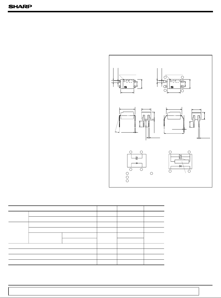
■ Outline Dimensions
(
Unit : mm
)
(
Ta = 25˚C
)
■ Absolute Maximum Ratings
Internal connection diagram
Zero-cross circuit
S11ME5/S21ME5/S21ME5F
S11ME5/S11ME6
S21ME5/S21ME6
S11ME6/S21ME6/S21ME6F
θ
S21ME5F/S21ME6F
0.5
Cathode
1 Anode
2 Cathode
3 Anode/
Cathode
4 Anode/
1
2
3434
12
❈ Lead forming type
(
I type
)
of / S21ME5F/ S21ME6F / S21ME5FI/
Parameter Symbol Rating Unit
Input
Forward current I
F
50 mA
Reverse voltage V
R
6V
Output
RMS ON-state current I
T
100 mA
rms
∗1
Peak one cycle surge current I
surge
1.2 A
Repetitive peak
OFF-state voltage
S11ME5/S11ME6
∗
2
S21ME5 /S21ME6
V
DRM
400
V
600
∗3
Isolation voltage V
iso
V
rms
Operating temperature T
opr
- 30 to +100 ˚C
Storage temperature T
stg
- 55 to +125 ˚C
∗4
Soldering temperature T
sol
260 ˚C
S21ME5F/ S21ME6F
5. Built-in zero-cross circuit
(
S11ME6/S21ME6/S21ME6F
)
S21ME5F,
(
Distance between lead pins : 10.16 mm
)
7. High isolation voltage between input and
output
S21ME6FI
)
1. Internal isolation distance : 0.4mm or more
6. Wide forming type
(
S21ME6F
)
∗1 50Hz sine wave ∗2 Also
3. Clearance : 6.4mm or more
2. Creepage distance : 6.4mm or more
Approved by BSI
(
BS415 : No.6690, BS7002 : No.7421
)
Approved by SEMKO
(
No.9202227
)
Approved by DEMKO
(
No.107968
)
Approved by EI
(
No.152029-02,03,04,0116
)
5 000
∗3 40 to 60%RH, AC for 1 minute, f= 60Hz
2.54
±
0.25
4.58
±
0.5
1.2
±
0.3
0.9
±
0.3
2.54
±
0.25
4.58
±
0.5
1.2
±
0.3
0.9
±
0.3
1
2
3
4
S11ME5 S21ME5
Anode mark
Anode mark
2.7
MIN
data books, etc. Contact SHARP in order to obtain the latest version of the device specification sheets before using any SHARP's device.”
“ In the absence of confirmation by device specification sheets, SHARP takes no responsibility for any defects that occur in equipment using any of SHARP's devices, shown in catalogs,
S11ME5/S11ME6/S21ME5/S21ME5F/S21ME6/S21ME6F
are also available.
(
❈ DIN-VDE0884 approved type is also available as an option.
(
Viso : 5 000V
rms
)
4. Recogized by UL file No. E64380
Approved by VDE
(
DIN-VDE0884 : No.76850
)
2.7
MIN
6.5
±
0.5
6.5
±
0.5
7.62
±
0.3
0.26
±
0.1
3.4
±
0.5
0.5
±
0.1
3.5
±
0.5
4.58
±
0.5
7.62
±
0.3
0.26
±
0.1
10.16
±
0.5
4.58
±
0.5
3.5
±
0.5
0.5
±
0.1
θ : 0 to 13˚
■ Electro-optical Characteristics
(
Ta = 25˚C
)
Parameter Symbol MIN. TYP. MAX. Unit
Input
Forward voltage V
F
- 1.2 1.4 V
Reverse current I
R
--10
-5
A
Repetitive peak OFF-state current
I
DRM
--10
-6
A
ON-state voltage V
T
- - 2.5 V
Holding current I
H
0.1 - 3.5 mA
Critical rate of rise of OFF-state voltage
100 - - V/µs
∗5
Zero-cross voltage V
OX
- - 35 V
Transfer
charac-
teristics
Minimum trigger current
Isolation resistance
Turn-on time
I
FT
- - 10 mA
R
ISO
5x10
10
10
11
- Ω
t
on
- - 100 µs
2
V
DRM
=
(
1/
)
• Rated
Conditions
I
F
= 20mA
V
R
=3V
V
DRM
= Rated
I
T
= 100mA
V
D
=6V
F
= 15mA
R
L
= 100Ω , V
D
=6V
V
D
= 6V, R
L
= 100Ω , I
F
= 20mA
-
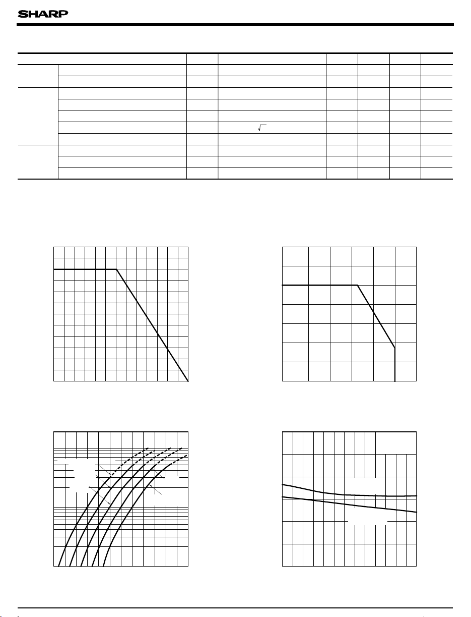
30 0 20406080100
0
Fig. 1 RMS ON-state Current vs.
Ambient Temperature
Ambient temperature T
a
(
˚C
)
-
30 0 25 75 100 125
0
10
30
40
50
60
70
Fig. 2 Forward Current vs.
Ambient Temperature
Forward current I
F
(
mA
)
Ambient temperature T
a
(
˚C
)
1
0.9
2
5
10
20
50
100
1.0 1.1 1.2 1.3 1.4 1.5
0˚C
-25˚C
50˚C
25˚C
Fig. 3 Forward Current vs. Forward Voltage
10
8
6
4
2
100806040200
0
-
30
12
S21ME5/5F
S11ME5
S21ME6/6F
S11ME6
Fig. 4 Minimum Trigger Current vs.
Ambient Temperature
T
(
mA
rms
)
∗5 S11ME6, S21ME6, S21ME6F
Forward voltage V
F
(
V
)
Forward current I
F
(
mA
)
FT
(
mA
)
Ambient temperature T
a
(
˚C
)
Output
20
40
60
80
100
120
RMS ON-state current I
20
50
Minimum trigger current I
Resistance load, I
DC = 500V, 40 to 60% RH
T
a
= 75˚C
R
L
= 100Ω
V
D
=6V
S11ME5/S11ME6/S21ME5/S21ME5F/S21ME6/S21ME6F
dV/dt
 Loading...