


 Loading...
QLED TV
Chassis : QNU70
Model : QN49Q6FAMF
QN55Q6FAMF
SERVICE Manual 
QLED TV |
|
Contents |
|
|
|
1. Precautions
2. Product specifications
3. Disassembly and Reassembly
4. Troubleshooting
5. Wiring Diagram
QN**Q6FAMF
|
|
Contents |
|
1. Precautions.................................................................................................................... |
1-1 |
||
1-1. |
Safety Precautions .............................................................................................................. |
1-1 |
|
|
1-1-1. Warnings................................................................................................................... |
1-1 |
|
|
1-1-2. Servicing the LED TV................................................................................................ |
1-1 |
|
|
1-1-3. |
Fire and Shock Hazard.............................................................................................. |
1-1 |
|
1-1-4. |
Product Safety Notices.............................................................................................. |
1-2 |
1-2. |
Servicing Precautions.......................................................................................................... |
1-3 |
|
|
1-2-1. |
General Servicing Precautions.................................................................................. |
1-3 |
1-3. |
Static Electricity Precautions................................................................................................ |
1-4 |
|
1-4. |
Installation Precautions........................................................................................................ |
1-5 |
|
2. Product Specifications................................................................................................. |
2-1 |
|
2-1. |
Product information.............................................................................................................. |
2-1 |
2-2. |
Product specification............................................................................................................ |
2-2 |
2-3. Accessories.......................................................................................................................... |
2-6 |
|
2-4. |
Viewing the Functions.......................................................................................................... |
2-7 |
|
2-4-1. 2017' Concept................................................................................................. |
2-7 |
|
2-4-2. TV Plus...................................................................................................................... |
2-8 |
|
2-4-3. Smart Features.......................................................................................................... |
2-9 |
|
2-4-4. The Samsung Smart Remote.................................................................................. |
2-12 |
3. Disassembly and Reassembly..................................................................................... |
3-1 |
3-1. Disassembly and Reassembly............................................................................................. |
3-1 |
4. Troubleshooting............................................................................................................ |
4-1 |
4-1. Previous Check ................................................................................................................... |
4-1 |
4-2. How to Check Fault Symptom.............................................................................................. |
4-2 |
4-2-1. Power........................................................................................................................ |
4-2 |
4-2-2. Video......................................................................................................................... |
4-8 |
4-2-3. One Connect............................................................................................................. |
4-9 |
4-2-4. Troubleshooting Video Problems............................................................................ |
4-10 |
4-2-5. Audio....................................................................................................................... |
4-14 |
4-2-6. Network................................................................................................................... |
4-15 |
4-2-7. Smart Hub............................................................................................................... |
4-16 |
4-2-8. Bluetooth / WiFi Module.......................................................................................... |
4-18 |
4-3. Factory Mode..................................................................................................................... |
4-19 |
4-4. Factory Mode Adjustments................................................................................................. |
4-24 |
4-4-1. Detail Factory Option............................................................................................... |
4-24 |
4-4-2. Factory Data............................................................................................................ |
4-26 |
4-5. AV Control Tabe................................................................................................................. |
4-39 |
4-6. Dimensions........................................................................................................................ |
4-46 |
4-7. Updating the TV’s Software............................................................................................... |
4-47 |
5. Wiring Diagram.............................................................................................................. |
5-1 |
||
5-1. |
Wiring Diagram.................................................................................................................... |
5-1 |
|
5-2. |
Connector............................................................................................................................. |
5-3 |
|
|
5-2-1. |
Main Board................................................................................................................ |
5-3 |
|
5-2-2. |
One Connect Board................................................................................................... |
5-8 |
|
5-2-3. |
SMPS Board............................................................................................................ |
5-10 |
ANNEX. Exploded View & Part List [QN49Q6FAMFXZA FA01].......................... |
ANNEX-1 |
|
1-1. |
Exploded View.......................................................................................................... |
ANNEX-1 |
|
1-1-1. Parts List........................................................................................................ |
ANNEX-1 |
1-2. ONE CONNECT Exploded View............................................................................... |
ANNEX-2 |
|
|
1-2-1. Parts List........................................................................................................ |
ANNEX-2 |
2-1. |
Electrical Parts List.................................................................................................... |
ANNEX-3 |
ANNEX. Exploded View & Part List [QN55Q6FAMFXZA FA01].......................... |
ANNEX-1 |
|
1-1. |
Exploded View.......................................................................................................... |
ANNEX-1 |
|
1-1-1. Parts List........................................................................................................ |
ANNEX-1 |
1-2. ONE CONNECT Exploded View............................................................................... |
ANNEX-2 |
|
|
1-2-1. Parts List........................................................................................................ |
ANNEX-2 |
2-1. |
Electrical Parts List.................................................................................................... |
ANNEX-3 |

This Service Manual is a property of Samsung Electronics Co.,Ltd.
Any unauthorized use of Manual can be punished under applicable International and/or domestic law.
© 2017 Samsung Electronics Co.,Ltd. All rights reserved.
Printed in Korea
1. Precautions
1. Precautions
1-1. Safety Precautions
Follow these safety, servicing and ESD precautions to prevent damage and to protect against potential hazards such as electrical shock.
1-1-1. Warnings
For continued safety, do not attempt to modify the circuit board.
WARNING |
Disconnect the AC power and DC power jack before servicing. |
|
1-1-2. Servicing the LED TV
1.When servicing the LED TV, Disconnect the AC line cord from the AC outlet.
2.It is essential that service technicians have an accurate voltage meter available at all times. Check the calibration of this meter periodically.
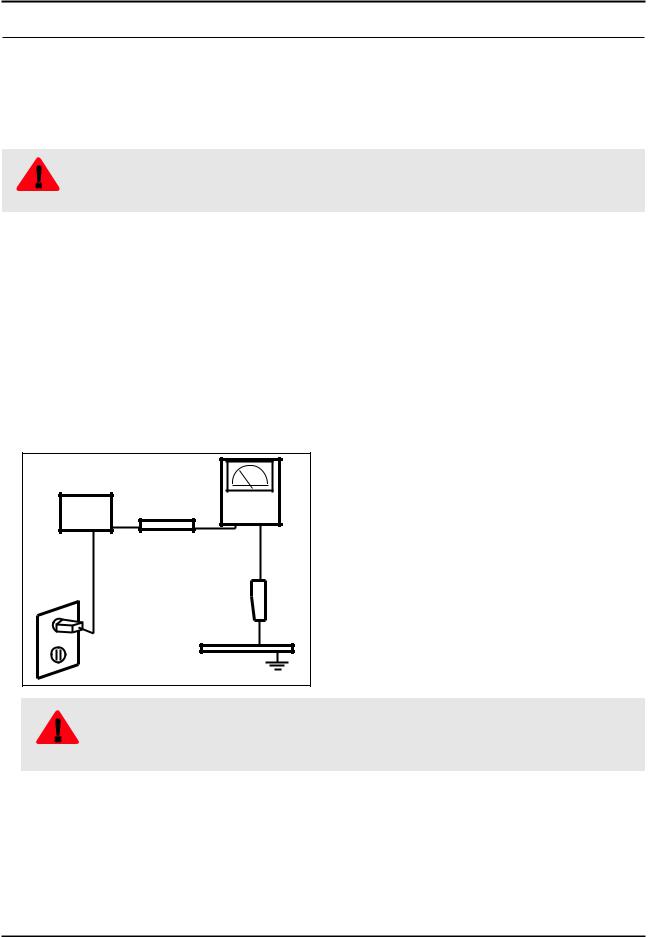
1-1-3. Fire and Shock Hazard
Before returning the monitor to the user, perform the following safety checks:
1.Inspect each lead dress to make certain that the leads are not pinched or that hardware is not lodged between the chassis and other metal parts in the monitor.
2.Inspect all protective devices such as nonmetallic control knobs, insulating materials, cabinet backs, adjustment and compartment covers or shields, isolation resistorcapacitor networks, mechanical insulators, etc.
3.Leakage Current Hot Check:
(READING SHOULD) |
|
|
NOT BE ABOVE 0.5mA |
LEAKAGE |
|
DEVICE |
||
CURRENT |
||
UNDER |
||
TESTER |
||
TEST |
||
|
||
TEST ALL |
|
|
EXPOSED METAL |
|
|
SURFACES |
|
|
2-WIRE CORD |
|
|
ALSO TEST WITH |
|
|
PLUG REVERSED |
EARTH |
|
(USING AC ADAPTER |
||
PLUG AS REQUIRED) |
GROUND |
Do not use an isolation transformer during this test.
|
Use a leakage current tester or a metering system that complies with American National Standards |
|
WARNING |
Institute (ANSI C101.1, Leakage Current for Appliances), and Underwriters Laboratories (UL |
|
Publication UL1410, 59.7). |
||
|
4.With the unit completely reassembled, plug the AC line cord directly into a 120V AC outlet. With the unit’s AC switch first in the ON position and then OFF, measure the current between a known earth ground (metal water pipe, conduit, etc.) and all exposed metal parts, including: metal cabinets, screwheads and control shafts.
The current measured should not exceed 0.5 milliamp.
Reverse the power-plug prongs in the AC outlet and repeat the test.
1-1

1. Precautions
1-1-4. Product Safety Notices
Some electrical and mechanical parts have special safetyrelated characteristics which are often not evident from visual inspection. The protection they give may not be obtained by replacing them with components rated for higher voltage, wattage, etc. Parts that have special safety characteristics are identified by  on schematics and parts lists. A substitute replacement that does not have the same safety characteristics as the recommended replacement part might create shock, fire and/or other hazards. Product safety is under review continuously and new instructions are issued whenever appropriate.
1-2

1. Precautions
1-2. Servicing Precautions
An electrolytic capacitor installed with the wrong polarity might explode.
WARNING
Before servicing units covered by this service manual, read and follow the Safety Precautions section of
this manual.
CAUTION
If unforeseen circumstances create conflict between the following servicing precautions and any of the
safety precautions, always follow the safety precautions.
NOTE
1-2-1. General Servicing Precautions
1.Always unplug the unit’s AC power cord from the AC power source and disconnect the DC Power Jack before attempting to: (a) remove or reinstall any component or assembly, (b) disconnect PCB plugs or connectors, (c) connect a test component in parallel with an electrolytic capacitor.
2.Some components are raised above the printed circuit board for safety. An insulation tube or tape is sometimes used. The internal wiring is sometimes clamped to prevent contact with thermally hot components. Reinstall all such elements to their original position.
3.After servicing, always check that the screws, components and wiring have been correctly reinstalled. Make sure that the area around the serviced part has not been damaged.
4.Check the insulation between the blades of the AC plug and accessible conductive parts (examples: metal panels, input terminals and earphone jacks).
5.Insulation Checking Procedure: Disconnect the power cord from the AC source and turn the power switch ON. Connect an insulation resistance meter (500 V) to theblades of the AC plug. The insulation resistance between each blade of the AC plug and accessible conductive parts (see above) should be greater than 1 megohm.
6.Always connect a test instrument’s ground lead to the instrument chassis ground before connecting the positive lead; always remove the instrument’s ground lead last.
1-3
1. Precautions
1-3. Static Electricity Precautions
Some semiconductor (solid state) devices can be easily damaged by static electricity. Such components are commonly called Electrostatically Sensitive Devices (ESD). Examples of typical ESD are integrated circuits and some field-effect transistors. The following techniques will reduce the incidence of component damage caused by static electricity.
1.Immediately before handling any semiconductor components or assemblies, drain the electrostatic charge from your body by touching a known earth ground. Alternatively, wear a discharging wrist-strap device. To avoid a shock hazard, be sure to remove the wrist strap before applying power to the monitor.
2.After removing an ESD-equipped assembly, place it on a conductive surface such as aluminum foil to prevent accumulation of an electrostatic charge.
3.Do not use freon-propelled chemicals. These can generate electrical charges sufficient to damage ESDs.
4.Use only a grounded-tip soldering iron to solder or desolder ESDs.
5.Use only an anti-static solder removal device. Some solder removal devices not classified as “anti-static” can generate electrical charges sufficient to damage ESDs.
6.Do not remove a replacement ESD from its protective package until you are ready to install it. Most replacement ESDs are packaged with leads that are electrically shorted together by conductive foam, aluminum foil or other conductive materials.
7.Immediately before removing the protective material from the leads of a replacement ESD, touch the protective material to the chassis or circuit assembly into which the device will be installed.
Be sure no power is applied to the chassis or circuit and observe all other safety precautions.
CAUTION
8.Minimize body motions when handling unpackaged replacement ESDs. Motions such as brushing clothes together, or lifting your foot from a carpeted floor can generate enough static electricity to damage an ESD.
1-4

1. Precautions
1-4. Installation Precautions
1.For safety reasons, more than a people are required for carrying the product.
2.Keep the power cord away from any heat emitting devices, as a melted covering may cause fire or electric shock.
3.Do not place the product in areas with poor ventilation such as a bookshelf or closet. The increased internal temperature may cause fire.
4.Bend the external antenna cable when connecting it to the product. This is a measure to protect it from being exposed to moisture. Otherwise, it may cause a fire or electric shock.
5.Make sure to turn the power off and unplug the power cord from the outlet before repositioning the product. Also check the antenna cable or the external connectors if they are fully unplugged. Damage to the cord may cause fire or electric shock.
6.Keep the antenna far away from any high-voltage cables and install it firmly. Contact with the highvoltage cable or the antenna falling over may cause fire or electric shock.
7.When installing the product, leave enough space (0.4m) between the product and the wall for ventilation purposes.
A rise in temperature within the product may cause fire.
8.If an equipment is provided with a replaceable battery, and if replacement by an incorrect type could result in an explosion (for example, with some lithium batteries), the following applies:
•Risk of explosion if battery is replaced by an incorrect type dispose of used batteries according to the instructions.
•Do not dispose of batteries in a fire.
•Do not short circuit, disassemble or overheat the batteries.
CAUTION • Danger of explosion if battery is incorrectly replaced. Replace only with the same or equivalent type.
•Do not be exposed to excessive heat such as sunshine, fire or the like.
1-5
2. Product specifications
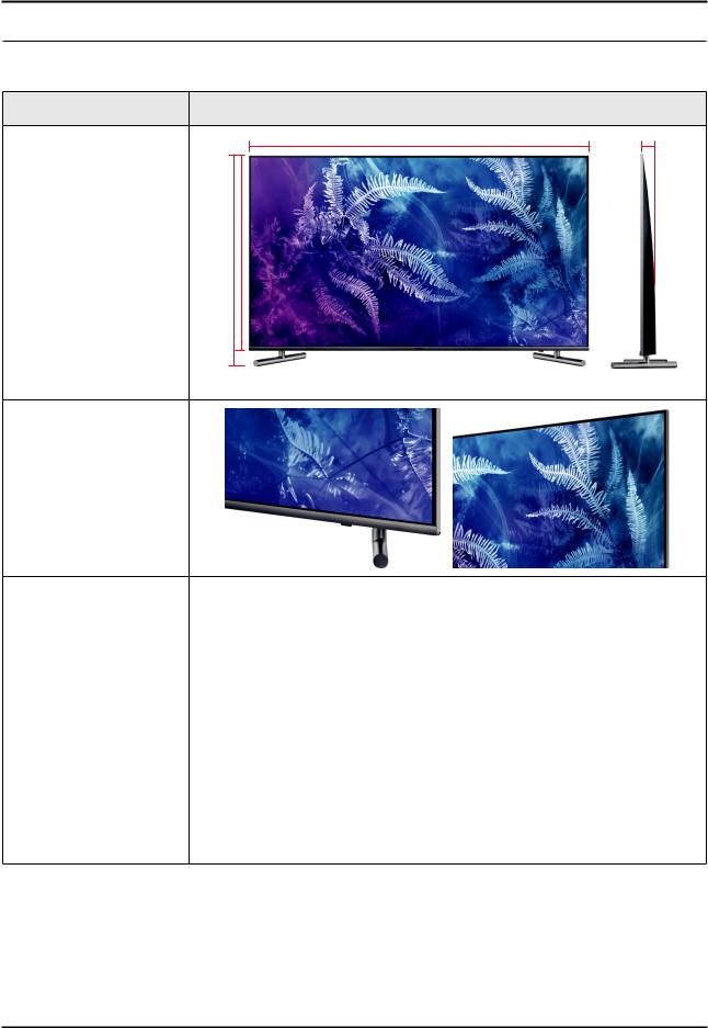
2. Product Specifications
2-1. Product information
Model |
QN**Q6FAMF |
W
Front View |
H |
* W : Width H : High D : Depth |
|
D |
Detail View
Color |
|
Front : DARK TITAN / Stand : DARK TITAN |
||
|
|
|
|
|
|
49" |
Body |
42.9 x 25.0 x 2.2 inches (1090.3 x 634.1 x 55.3 mm) |
|
|
|
|
||
Dimensions |
With Stand |
42.9 x 26.4 x 8.3 inches (1090.3 x 669.9 x 209.9 mm) |
||
|
||||
|
|
|
||
(W x H x D) |
55" |
Without Stand |
48.3 x 28.0 x 2.2 inches (1226.1 x 710.5 x 54.8 mm) |
|
|
||||
|
|
|
||
|
With Stand |
48.3 x 29.4 x 8.3 inches (1226.1 x 746.1 x 209.9 mm) |
||
|
|
|||
|
|
|
|
|
|
49" |
Body |
31.5 lbs (14.3 kg) |
|
|
|
|
||
Weight |
With Stand |
32.6 lbs (14.8 kg) |
||
|
||||
|
|
|
||
55" |
Without Stand |
38.4 lbs (17.4 kg) |
||
|
||||
|
|
|
||
|
With Stand |
39.5 lbs (17.9 kg) |
||
|
|
|||
|
|
|
|
|
Flash |
|
|
8GB (eMMC 5.0) |
|
|
|
|
|
|
DDR |
|
|
LPDDR4 64bit @1.6GHz |
|
2-1
2. Product specifications
2-2. Product specification
 NOTE
NOTE
Design and specifications are subject to change without prior notice.
|
|
Last Update Date : 2017.09.21 |
|
|
|
|
Item |
QN49Q6FAMFXZA |
|
|
|
General Information |
Product |
QLED |
|
|
|
|
Series |
6 |
|
|
|
|
Country |
UNITED STATES |
|
|
|
Display |
Screen Size |
49" |
|
|
|
|
Q Display |
Yes |
|
|
|
|
Resolution |
3,840 × 2,160 |
|
|
|
|
Ultra Black |
N/A |
|
|
|
|
Screen Curvature |
N/A |
|
|
|
|
10 bit Support |
N/A |
|
|
|
Video |
Picture Engine |
UHD Upscaling Engine |
|
|
|
|
Motion Rate |
120 |
|
|
|
|
HDR (High Dynamic Range) |
Q ] 4K HDR Extreme |
|
|
|
|
Blacks |
N/A |
|
|
|
|
Dynamic Contrast Ratio |
Mega Contrast |
|
|
|
|
Q Every View |
N/A |
|
|
|
|
Micro Dimming |
UHD Dimming |
|
|
|
|
Local Dimming |
Precision Black |
|
|
|
|
Q Color |
Q ] 4K Color Drive Extreme |
|
|
|
|
Auto Depth Enhancer |
N/A |
|
|
|
|
Contrast Enhancer |
Yes |
|
|
|
|
Auto Motion Plus |
Yes |
|
|
|
|
Film Mode |
Yes |
|
|
|
|
Natural Mode Support |
Yes |
|
|
|
|
Peak Illuminator |
Peak Illuminator Pro |
|
|
|
Audio |
Dolby Digital Plus |
Yes |
|
|
|
|
DTS Codec |
Yes |
|
|
|
|
Sound Output (RMS) |
40W |
|
|
|
|
Speaker Type |
2.1CH (Down Firing) |
|
|
|
|
Woofer |
Yes |
|
|
|
|
Multiroom Link |
Yes |
|
|
|
|
Blutooth Audio |
Yes |
|
|
|
Smart Service |
Voice Interaction |
US English, Spanish, French |
|
|
|
|
TV Plus |
Yes(US only. App) |
|
|
|
2-2

|
|
2. Product specifications |
|
|
|
|
|
|
|
Item |
QN49Q6FAMFXZA |
|
|
|
Smart Service |
Web Browser |
Yes |
|
|
|
|
Samsung Connect |
Yes |
|
|
|
|
Smart View |
Yes |
|
|
|
Convergence |
TV to Mobile - Mirroring |
Yes |
|
|
|
|
Mobile to TV - Mirroring, DLNA |
Yes |
|
|
|
|
360 Video Player |
Yes |
|
|
|
|
360 Camera Support |
N/A |
|
|
|
|
Bluetooth Low Energy |
Yes |
|
|
|
|
RVU |
Yes |
|
|
|
|
WiFi Direct |
Yes |
|
|
|
|
TV as Hub Support |
N/A |
|
|
|
|
TV as Things Support |
N/A |
|
|
|
|
IoT Client Application (SmartThings App) |
N/A |
|
|
|
Tuner/Broadcasting |
Digital Broadcasting |
ATSC/ClearQAM |
|
|
|
|
Analog Tuner |
Yes |
|
|
|
|
TV Key Support |
N/A |
|
|
|
Connectivity |
HDMI |
4 |
|
|
|
|
USB |
3 |
|
|
|
|
Component In (Y/Pb/Pr) |
N/A |
|
|
|
|
Composite In (AV) |
N/A |
|
|
|
|
Ethernet (LAN) |
Yes |
|
|
|
|
Audio Out (Mini Jack) |
N/A |
|
|
|
|
Digital Audio Out (Optical) |
1 |
|
|
|
|
RF In (Terrestrial / Cable input / Satellite input) |
1/1(Common Use for Terrestrial)/0 |
|
|
|
|
Ex-Link ( RS-232C ) |
1 |
|
|
|
|
CI Slot |
N/A |
|
|
|
|
HDMI A / Return Ch. Support |
Yes |
|
|
|
|
HDMI Quick Switch |
Yes |
|
|
|
|
Wireless LAN Built-in |
Yes |
|
|
|
|
Anynet+ (HDMI-CEC) |
Yes |
|
|
|
Design |
Design |
Slim Edge |
|
|
|
|
Bezel Type |
3 Bezel-less |
|
|
|
|
Front Color |
Dark Titan |
|
|
|
|
Light Effect (Deco) |
N/A |
|
|
|
|
Stand Type |
Branch |
|
|
|
|
Swivel (Left/Right) |
N/A |
|
|
|
Additional Feature |
Instant On |
Yes |
|
|
|
|
Processor |
Quad-Core |
|
|
|
2-3

2. Product specifications
|
Item |
QN49Q6FAMFXZA |
|
|
|
Additional Feature |
|
Voice Guide(US English)/ Enlarge/ High |
|
Accessibility |
Contrast/ Learn TV Remote(US English)/ Multi- |
|
|
output Audio |
|
One Connect |
One Connect Mini |
|
|
|
|
Digital Clean View |
Yes |
|
|
|
|
Auto Channel Search |
Yes |
|
|
|
|
Auto Power Off |
Yes |
|
|
|
|
Caption (Subtitle) |
Yes |
|
|
|
|
Connect Share™ (HDD) |
Yes |
|
|
|
|
ConnectShare™ (USB 2.0) |
Yes |
|
|
|
|
Embeded POP |
Yes |
|
|
|
|
EPG |
Yes |
|
|
|
|
Game Mode |
Yes |
|
|
|
|
OSD Language |
English, Spanish, French |
|
|
|
|
BT HID Built-in |
Yes |
|
|
|
|
USB HID Support |
Yes |
|
|
|
|
V-Chip |
Yes |
|
|
|
|
IPv6 Support |
Yes(US) |
|
|
|
|
Ultra Clean View |
Yes |
|
|
|
Eco Feature |
Eco Sensor |
Yes |
|
|
|
|
Energy Star |
Yes |
|
|
|
2-4

|
|
2. Product specifications |
|
|
|
|
|
|
|
Item |
QN55Q6FAMFXZA |
|
|
|
General Information |
Product |
QLED |
|
|
|
|
Series |
6 |
|
|
|
|
Country |
UNITED STATES |
|
|
|
Display |
Screen Size |
55" |
|
|
|
no data
2-5
2. Product specifications
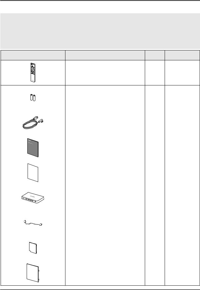
2-3. Accessories
 NOTE
NOTE
•The items’ colors and shapes may vary depending on the model.
•Cables not included in the package contents can be purchased separately.
•The part code for some accessories may differ depending on your region.
•The provided accessories may vary depending on the model.
Image |
Product |
Inches |
Code. No |
• |
Samsung Smart Remote |
All |
BN59-01292A |
• |
Batteries (AA x 2) |
All |
4301-000101 |
|
|
|
|
|
|
• |
Power Cord |
All |
3903-001209 |
|
|
|
|
|
|
|
|
49" |
BN68-07509K |
|
• |
User Manual |
|
|
|
55" |
BN68-07450S |
|||
|
|
|||
|
|
|
|
|
• |
Regulatory Guide |
All |
BN68-08114Q |
|
|
|
|
|
|
|
|
49" |
BN91-19624A |
|
• |
One Connect |
|
|
|
55" |
BN91-19624D |
|||
|
|
|||
|
|
|
|
|
|
|
49" |
BN39-02248B |
|
• |
One Connect Cable |
|
|
|
55" |
BN39-02210C |
|||
|
|
|||
|
|
|
|
|
|
|
49" |
BN63-16645A |
|
• |
CLEAN BACK TERMINAL |
|
|
|
55" |
BN63-16646A |
|||
|
|
|||
|
|
|
|
|
|
|
49" |
BN96-43019A |
|
• CLEAN BACK AC INLET |
|
|
||
55" |
BN96-42851A |
|||
|
|
|||
2-6

2. Product specifications
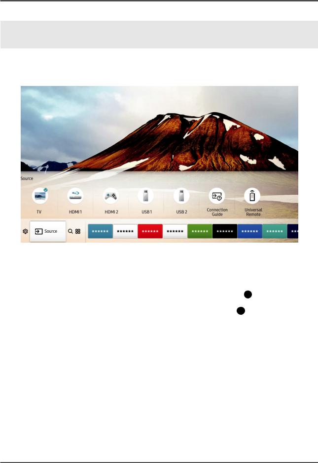
2-4. Viewing the Functions
2-4-1. 2017' Concept
[Quick Setting] |
[Sources] |
[Apps] |
[Live TV] |
2-7

2. Product specifications
2-4-2. TV Plus
[TV Shows]
[Movies]
[Samsung Check-Out]
2-8
2. Product specifications
2-4-3. Smart Features
 NOTE
NOTE
•The image on your TV may differ from the image above depending on your model and geographical area.
Smart Hub
View descriptions of Smart Hub's basic functions.
After pressing the  button on your remote control, you can surf the web and download apps with Smart Hub.
•Some of the Smart Hub services are paid services.
•To use Smart Hub, the TV must be connected to the Internet.
•Some Smart Hub features may not be available depending on the service provider, language, or region.
•Smart Hub service outages can be caused by disruptions in your Internet service.
•You can view the entire text of the Terms and Privacy Policy document by navigating to  £
£  Settings £ Support £ Terms and Privacy Policy. If you want to stop using Smart Hub, you can cancel the agreement.
•To cancel the Smart Hub service agreement though it is a required one, select Reset (  £
£  Settings £ General £ Support £ Self Diagnosis £ Reset), and then press the right directional button at the Smart Hub Terms & Conditions, Privacy Policy step.
2-9

2. Product specifications
APPS
Download and run various apps from Smart Hub.
 £ š Apps
You can enjoy a wide range of content including news, sports, weather, and games by installing the corresponding apps on your TV.
•To use this feature, the TV must be connected to the Internet.
•When Smart Hub is launched for the first time, the default apps are automatically installed. The default apps may differ with the geographical area.
2-10

2. Product specifications
Pictures/Video/Music
Play media content stored on your TV, USB devices, smartphones, cameras, PCs, etc.
 £ s Source £ Connected Device
You can play media content saved on storage devices, such as USB devices, mobile devices, and cameras, on the TV.
•You cannot play media content if the content or the storage device is not supported by the TV. For more information, refer to "Read Before Playing Photo, Video, or Music Files."
•To connect the TV to a computer, refer to "Connecting a Computer."
•Backup important files before connecting a USB device. Samsung is not responsible for damaged or lost files.
•To connect the TV to a mobile device, refer to "Connecting a Mobile Device."
2-11

2. Product specifications
2-4-4. The Samsung Smart Remote
Pairing the TV to the Samsung Smart Remote
When you turn on the TV for the first time, the Samsung Smart Remote pairs to the TV automatically. If the Samsung Smart Remote does not pair to the TV
automatically, point it at the remote control sensor of the TV, and then press and hold the buttons labeled  and
and  as shown in the figure on the left simultaneously for 3 seconds or more.
2-12
3. Disassembly and Reassemble
3. Disassembly and Reassembly
This section of the service manual describes the disassembly and reassembly procedures for the LED TV.
1.Disconnect the LED TV from the power source before disassembly.
2.Follow these directions carefully.
-- Use the Samsung Service tool to disassemble the cabinet.
CAUTION |
• Recommend to use the Samsung Service tool. |
|
-- Recommended Torque for Cabinet/Stand screws : 10 ~ 12kgf |
||
|
•A strength of Torque can be changed depending on the situation.
Required Jigs & Tools
|
• Open Jig Tool |
BN81-14946A |
|
|
|
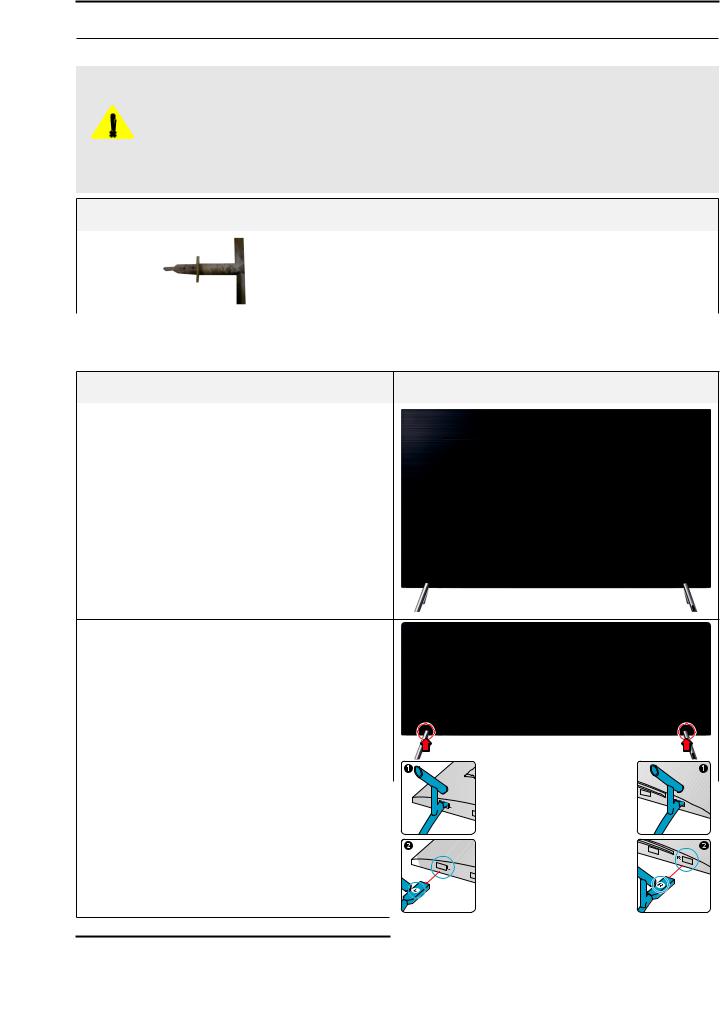
3-1. Disassembly and Reassembly
|
Description & Screws |
Picture Description |
|
|
|
1 |
Carefully position the TV so that the screen is |
|
facing downwards. Make sure to place the TV |
|
|
|
upon a soft cushion or any material that will |
|
|
prevent damage to the screen. |
|
|
• Place TV face down on the Protective Cushion. |
|
2 |
Remove the ASSY STAND P-BOTTOM (R/L) |
with pulling it down. |
3-1

3. Disassembly and Reassemble |
|
|
|
|
|
||
|
|
Description & Screws |
|
|
Picture Description |
|
|
3 |
Use Open Jig to release tape in corners and |
|
|
Jig Direction |
|
||
all clips as indicated in red on sides and top & |
|
|
|
||||
|
bottom. |
|
|
|
|
|
|
|
Gently lift up the Rear Cover starting at the top |
|
|
|
|
||
|
being careful of function assembly at the bottom. |
|
|
|
|
||
|
• |
When the Upper 4 points ( |
)Hook is |
|
|
|
|
|
|
broken. |
|
|
|
|
|
|
|
Although the hook is broken, the appearance |
|
|
|
|
|
|
|
of the Rear cover is no problem and Gap |
Direction |
|
|
Direction |
|
|
• To prevent the Inner Hook's broken. |
|
|
||||
|
|
problem is not appeard after re-assembly. |
|
|
|
|
|
|
|
1. Catch the upper section of the rear cover. |
Jig |
|
|
Jig |
|
|
|
2. Open the rear cover from top to bottom. |
|
|
|
|
|
|
|
• If the wire is bent, need to change the wire. |
|
|
|
|
|
|
|
|
|
|
Top : 10 point Locking |
|
|
|
|
|
|
Locking |
Center : 1 Point Locking |
Locking |
|
|
|
|
|
L : 6 point |
R : 6 point |
||
|
|
|
|
|
|
||
|
|
|
|
|
Bottom : 4 point Locking |
|
|
|
• Panel Back Side View |
|
|
|
|
|
|
|
|
-- 49 / 55 inches |
|
|
|
|
|
4 |
Remove the Electric tapes, Remove them. |
|
|
|
|
||
|
|
NOTE |
|
|
|
|
|
|
|
• When assembling the TV, the electric tapes |
|
|
|
|
|
|
|
must be applied on the same locations. |
|
|
|
|
|
|
|
Please remember to take a picture of |
|
|
|
|
|
|
|
where the tapes were first applied. |
|
|
|
|
|
|
|
• When assembling the Boards, please make |
|
|
|
|
|
|
|
sure All Board Mounting Clips are securly |
|
|
|
|
|
|
|
inserted. |
|
|
|
|
|
|
|
|
|
Caution |
Dressing |
Sliding Fixing Point |
Filament Tape |
3-2

|
|
|
3. Disassembly and Reassemble |
|
|
|
|
|
|
|
|
|
|
Description & Screws |
Picture Description |
|
|
|
|
5 |
Remove the ASSY BOARD P-FUNCTION. |
ASSY BOARD P-FUNCTION Cable |
|
• |
ASSY BOARD P-FUNCTION Cable |
|
|
|
|
|
ASSY BOARD P-FUNCTION |
|
|
|
|
6 |
Remove the NETWORK. |
NETWORK Cable |
|
• |
NETWORK Cable |
|
|
|
|
|
NETWORK |
|
|
|
|
7 |
Remove the ASSY SPEAKER P-FRONT. |
ASSY SPEAKER P-FRONT Cable |
|
• |
ASSY SPEAKER P-FRONT Cable |
|
|
|
|
ASSY SPEAKER P-FRONT (49 / 55 inches) |
8 Remove the All Cables. |
Power Cable |
|
|
||
• 49 / 55 inches |
|
|
-- |
Power Cable |
|
-- |
USI-T Cables |
|
USI-T Cables
3-3
3. Disassembly and Reassemble
|
Description & Screws |
Picture Description |
||
|
|
|
|
|
9 |
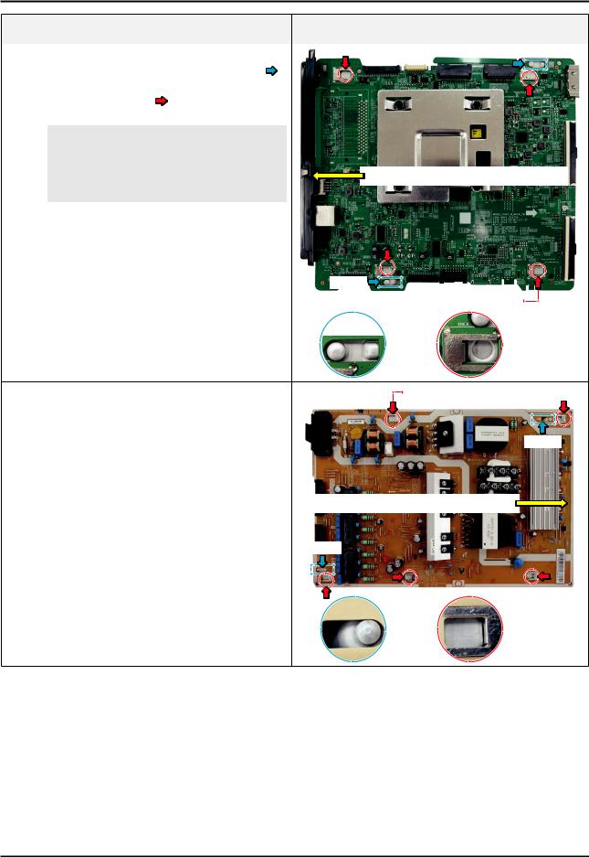
Remove the ASSY PCB MAIN BOARD. |
|
|
|
• Gently lift up to release the lock (Locking ). |
|
Locking |
|
|
|
|
|||
• Use both hands to hold (Bottom chassis Guide Fixing Hole ) the board and slide to the left to release the board.
 NOTE
NOTE
When installing the ASSY PCB MAIN BOARD,
verify the board is properly positioned in all 4 Slide to the left to release the board mounting slots.
|
|
Locking |
|
|
|
Bottom chassis Guide Fixing Hole |
|
|
|
Locking |
Fixing Hole |
10 |
Remove the DC VSS-PD BOARD. |
Bottom chassis Guide Fixing Hole |
|
• Use both hands to hold the SMPS and gently |
|
|
|
|
lift up at point indicated by the arrow to |
|
|
|
release the lock. |
|
Locking |
|
-- 49 / 55 inches |
|
|
|
|
|
|
|
|
Slide to the right to release the board |
|
|
|
Locking |
|
Locking |
Fixing Hole |
3-4

3. Disassembly and Reassemble
Description & Screws |
Picture Description |
11 Completed the disassembly.
 NOTE
NOTE
Reassembly procedures are in the reverse order of disassembly procedures.
3-5
4. Troubleshooting
4. Troubleshooting
4-1. Previous Check
Check list for initial operation
1.Check the various cable connections first.
-- Check to see if there is a burnt or damaged cable.
-- Check to see if there is a disconnected or loose cable connection.
-- Check to see if the cables are connected according to the connection diagram.
2.Check the power input to the Main Board.
3.How to distinguish if the problem is caused by Main Board.
-- No Video
Symptom |
If the problem is No Video but BLU is on and Indication LED is blinking repeatedly and faster |
|
than nomal booting. |
||
|
||
Check Points |
• Replace the Main Board. |
-- Distorted Picture :
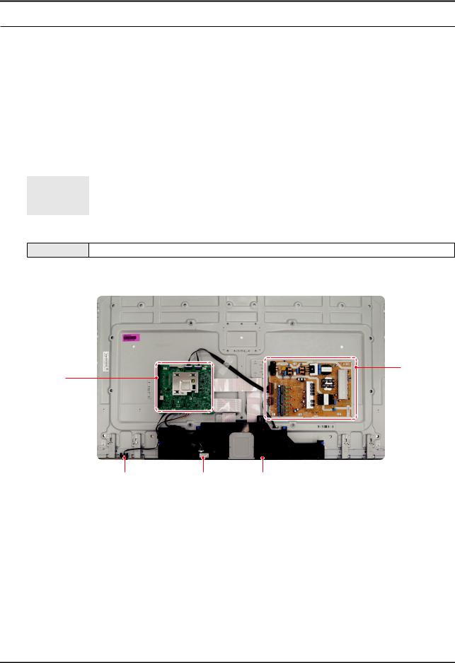
Check Points • Check the inner patterns.
Inner View
|
DC VSS-PD |
ASSY PCB MAIN |
BOARD |
ASSY BOARD P-FUNCTION NETWORK |
ASSY SPEAKER P-FRONT |
4-1

4. Troubleshooting
4-2. How to Check Fault Symptom
4-2-1. Power
FUNCTION/IR Control
CN1601 (FUNCTION/IR)

1 |
IR_TX_OCM |
7 |
KEY_INPUT2 |
2 |
DGND |
8 |
LED_STB_OUT |
|
|
|
|
3 |
A3.3V_PW |
9 |
A3.3V_PW |
|
|
|
|
4 |
IRB_SCL_I2C |
10 |
NC |
5 |
IRB_SDA_I2C |
11 |
NC |
|
|
|
|
6 |
KEY_INPUT1 |
12 |
NC |
|
|
|
|
 LED Status / Function Switch
<Function/IR>
1.TV in Standby
99 LED Status
2.If LED is OFF
99 LED 1.7Vdc (pin 8) and VCC for 3.3Vdc (pin 3)
•If missing suspect Function Assy/Cable Assy/Main Board.
3.If LED is ON
99 Switch Operation activates on screen display.
[On Screen Selections with Function Control]
-- If missing:
99 Key _Input1 Pin 6 change to 0V with a command.
-- If wrong voltage or no change:
99 Switch for stuck or miss-operation.
4.Check IR operation with Standard Remote command changes. (3.3V to 2.5V effective DC)
5.SDA, SCL for effective 3.3Vdc (after power on)
-- If missing suspect Function Assy/Cable Assy/Main Board.
4-2

4. Troubleshooting
SMPS Power
SMPS Front : 49 / 55 inches
|
|
|
|
|
CN9003 (MAIN Connector) |
|
|
|
|
|||
1 |
GND |
2 |
GND |
3 |
|
GND |
4 |
GND |
5 |
Vamp |
6 |
GND |
|
|
|
|
|
|
|
|
|
|
|
|
|
7 |
Vamp |
8 |
OD_Level |
9 |
|
Vamp |
10 |
Fail Count |
11 |
A13V |
12 |
OD_ON/OFF |
|
|
|
|
|
|
|
|
|
|
|
|
|
13 |
A13V |
14 |
BLUEON/OFF |
15 |
|
A13V |
16 |
PS_ON/OFF |
17 |
A13V |
18 |
GND |
|
|
|
|
|
|
|
|
|
|
|
|
|
19 |
GND |
20 |
GND |
21 |
|
PWM8 |
22 |
PWM7 |
23 |
PWM6 |
24 |
PWM5 |
|
|
|
|
|
|
|
|
|
|
|
|
|
25 |
PWM4 |
26 |
PWM3 |
27 |
|
GND |
28 |
PWM2 |
29 |
PWM1 |
30 |
ANA_DIM |
|
|
|
|
|
|
|
|
|
|
|
|
|
|
CNL801 (LED Connector) |
Fuse |
|||
|
|
||||
1 |
IF2 |
2 |
IF1 |
|
|
3 |
1+ |
4 |
5+ |
|
|
5 |
1- |
6 |
5- |
CN9003 |
|
7 |
2+ |
8 |
6+ |
||
|
|||||
9 |
2- |
10 |
6- |
|
|
11 |
3+ |
12 |
7+ |
CNL801 |
|
13 |
3- |
14 |
7- |
||
|
|||||
15 |
4+ |
16 |
8+ |
|
|
17 |
4- |
18 |
8- |
|
|
4-3

4. Troubleshooting
TV POWER STANDBY
1. TV in Standby
Standby LED Indicator
-- If Not Lit:
99 AC 120Vac Line -- If missing:
99 120Vac Source and Power Cord -- If OK:
99 Resistance on SMPS Fuse after first removing AC power cord.
2.If fusses are open replace SMPS.
-- If fuses are OK:
99 Standby: A13V (Always On) to Main Board.
-- If any missing remove the SMPS connector to Main Board . 99 Standby A13V again.
•If OK replace Main Board.
•If still missing replace SMPS.
4-4
Loading...