


Optoisolators (Photocouplers)
CNC7S101,CNZ3182,CNC7T101,CNC1H101
Optoisolators |
|
|
|
|
|
|
|
|
|
Overview |
|
|
|
CNC7S101 |
|
|
|
Unit : mm |
|
|
|
|
|
5.2 max. |
|
||||
CNC7S101 is an AC input compatible optoisolator in which two |
LED Mark |
0.5 min. |
|
2.54 min. |
|||||
|
|
|
|||||||
±0.3 |
|
|
|
|
|
||||
GaAs high output infrared light emitting diode chips are connected |
1 |
4 |
|
1: Anode/Cathode±4-0.50.1±4-1.20.15±2.540.25 |
|||||
|
|
|
|
0.33.85± 4.58 |
2.0 |
0.25–0 |
|
||
in reverse parallel as light emitting elements, and opitically are |
|
2 |
3 |
|
|
|
|||
|
7.62±0.3 |
+0.15 |
|
|
|
||||
connected to a high sensitivity Si phototransistor chip as a light |
|
6.2±0.5 |
|
|
|
|
|||
detecting element in a small DIL 4-pin package. |
|
|
|
|
|
|
|
||
This optoisolator series also includes the two-channel CNZ3182, |
|
15˚ |
|
15˚ |
2: Cathode/Anode |
||||
|
|
|
|
|
to |
to |
|||
the three-channel CNC7T101, and the four-channel CNC1H101. |
|
0 |
0 |
|
3: Emitter |
||||
|
|
|
|
||||||
|
|
|
|
4: Collector |
|||||
|
|
|
|
|
|
|
|
||
The CNC7S101 series has a number of excellent features, |
CNZ3182 |
|
5.2 max. |
Unit : mm |
|||||
including high I/O isolation voltage and current transfer ratio (CTR), |
|
|
|||||||
LED Mark |
0.5 min. |
|
2.54 min. |
||||||
as well as high speed response and high reliability. |
|
|
|
||||||
|
1 |
5 |
|
|
|
||||
|
|
|
|
0.3 |
|
|
|
||
|
|
|
|
2 |
6 |
|
|
|
|
Features |
|
|
|
9.66± |
|
|
-80.5±0.1 1.2-8 ±0.15 2.54±0.25 |
||
|
|
|
3 |
7 |
|
|
|||
|
|
|
|
4 |
+0.15 –0 |
|
|
||
AC input support |
|
|
|
|
7.62±0.3 |
|
|
|
|
High I/O isolation voltage : VISO = 5000 Vrms |
(min.) |
0.3 |
6.2±0.5 |
0.25 |
|
|
|
||
|
|
|
|
||||||
Fast response : tr = 4 μs, tf = 3 μs |
|
|
|
|
|
||||
|
3.85± |
2.0 |
|
|
1,3: Anode/Cathode |
||||
UL listed (UL File No. E79920) |
|
|
|
15˚ |
0 |
15˚ |
2,4: Cathode/Anode |
||
|
|
|
0 |
|
|
|
|||
|
|
|
|
|
to |
to |
5,7: Emitter |
||
|
|
|
|
|
|
|
|
||
|
|
|
|
|
|
|
|
6,8: Collector |
|
Applications |
|
|
|
CNC7T101 |
|
5.2 max. |
Unit : mm |
||
Telephones |
|
|
|
LED Mark |
0.5 min. |
|
2.54 min. |
||
|
|
|
|
|
|
||||
Telephone switches |
|
|
|
|
1 |
12 |
|
|
|
|
|
|
14.74±0.3 |
2 |
11 |
|
|
|
|
|
|
|
|
|
|
±0.10.5-12 ±0.151.2-12 ±0.252.54 |
|||
Programmable controllers |
|
|
3 |
10 |
|
|
|||
|
|
|
|
|
|
||||
|
|
|
4 |
9 |
|
|
|
||
|
|
|
|
|
|
|
|
||
AC/DC input modules for measuring |
|
|
5 |
8 |
|
|
|
||
|
|
|
|
|
6 |
7 |
|
|
|
|
|
|
|
|
7.62±0.3 |
+0.15 –0 |
|
|
|
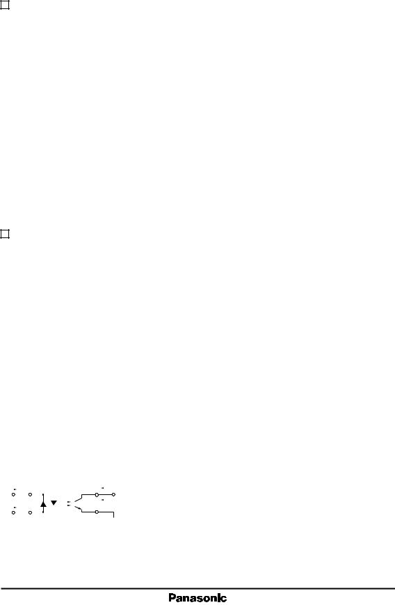
Pin Connection |
|
|
|
|
6.2±0.5 |
|
|
|
|
|
|
|
0.3 |
0.25 |
|
|
|
||
|
|
|
|
|
|
|
|
||
CNC7S101 |
|
CNZ3182 |
|
3.85± |
2.0 |
|
|
1,3,5: Anode/Cathode |
|
|
|
1 |
8 |
|
15˚ |
|
15˚ |
2,4,6: Cathode/Anode |
|
|
|
|
to |
to |
|
|
|||
|
|
|
|
|
0 |
0 |
|
7,9,11: Emitter |
|
|
|
|
|
|
|
|
|
||
1 |
4 |
2 |
7 |
|
|
|
|
8,10,12: Collector |
|
|
|
|
|
|
|
|
Unit : mm |
||
2 |
3 |
3 |
6 |
CNC1H101 |
|
5.2 max. |
|||
|
|
||||||||
|
|
LED Mark |
0.5 min. |
|
2.54 min. |
||||
|
|
|
|
|
|||||
|
|
|
|
|
|
|
|||
|
|
4 |
5 |
|
1 |
16 |
|
|
|
|
Top View |
|
Top View |
|
2 |
15 |
|
|
|
|
|
|
|
0.519.82± |
|
|
±0.10.5-16 ±0.151.2-16 ±0.252.54 |
||
CNC7T101 |
|
CNC1H101 |
|
3 |
14 |
|
|
||
|
|
|
|
|
|
||||
|
|
|
4 |
13 |
|
|
|
||
|
|
1 |
16 |
|
5 |
12 |
|
|
|
1 |
12 |
|
|
|
6 |
11 |
|
|
|
2 |
15 |
|
7 |
10 |
|
|
|
||
|
|
|
|
|
|
||||
|
|
3 |
14 |
|
8 |
9 |
|
|
|
2 |
11 |
|
7.62±0.3 |
+0.15 –0 |
|
|
|
||
|
|
|
|
|
|
||||
3 |
10 |
|
|
|
6.2±0.5 |
|
|
|
|
4 |
13 |
0.3 |
0.25 |
|
|
|
|||
|
|
|
|
||||||
|
|
|
|
|
|
||||
|
|
|
|
|
|
|
|
||
4 |
9 |
5 |
12 |
3.85± |
2.0 |
|
1,3,5,7: Anode/Cathode |
||
|
|
|
|
|
15˚ |
|
15˚2,4,6,8: Cathode/Anode |
||
5 |
8 |
|
|
|
to |
to |
|
|
|
6 |
11 |
|
0 |
0 |
9,11,13,15: Emitter |
||||
|
|
|
|||||||
|
|
|
|
|
|||||
|
|
7 |
10 |
|
|
|
10,12,14,16: Collector |
||
6 |
7 |
|
|
|
|
|
|
||
|
|
|
|
|
|
|
|
||
|
|
8 |
9 |
|
|
|
|
|
|
|
Top View |
|
Top View |
|
|
|
|
|
|
|
|
|
|
|
|
|
|
|
1 |
Optoisolators (Photocouplers) |
|
CNC7S101,CNZ3182,CNC7T101,CNC1H101 |
|||||||||||||||||||||||||||||||||||||
|
|
Absolute Maximum Ratings (Ta = 25˚C) |
|
|
|
|
|
|
|
|
|
|
|
|
|||||||||||||||||||||||||
|
|
|
|
|
|
|
|
|
|
|
|
|
|
||||||||||||||||||||||||||
|
|
|
|
|
|
|
|
|
|
|
|
|
|
|
|
|
|
|
|
|
|
|
|
|
|
|
|
||||||||||||
|
|
|
|
|
|
|
|
Parameter |
Symbol |
|
Ratings |
|
Unit |
|
|
|
|
|
|
|
|
|
|
||||||||||||||||
Input (Light |
|
|
|
|
|
Forward current (DC) |
IF |
|
|
±50 |
|
mA |
|
|
|
|
|
|
|
|
|
|
|||||||||||||||||
|
|
|
|
|
Pulse forward current |
IFP*1 |
|
|
±1 |
|
A |
|
|
|
|
|
|
|
|
|
|
||||||||||||||||||
emitting diode) |
|
|
|
|
|
|
|
|
|
|
|
|
|||||||||||||||||||||||||||
|
|
PD*2 |
|
|
75 |
|
mW |
|
|
|
|
|
|
|
|
|
|
||||||||||||||||||||||
|
|
|
|
|
|
|
|
|
|
Power dissipation |
|
|
|
|
|
|
|
|
|
|
|
|
|||||||||||||||||
|
|
|
|
|
|
|
|
|
|
Collector current |
IC |
|
|
50 |
|
mA |
|
|
|
|
|
|
|
|
|
|
|||||||||||||
Output (Photo |
Collector to emitter voltage |
VCEO |
|
|
80 |
|
V |
|
|
|
|
|
|
|
|
|
|
||||||||||||||||||||||
transistor) |
|
|
|
|
|
Emitter to collector voltage |
VECO |
|
|
7 |
|
V |
|
|
|
|
|
|
|
|
|
|
|||||||||||||||||
|
|
|
|
|
|
|
|
|
|
Collector power dissipation |
PC*3 |
|
|
150 |
|
mW |
|
|
|
|
|
|
|
|
|
|
|||||||||||||
Total power dissipation |
PT |
|
|
200 |
|
mW |
|
|
|
|
|
|
|
|
|
|
|||||||||||||||||||||||
Isolation voltage, input to output |
*4 |
|
|
5000 |
|
Vrms |
|
|
|
|
|
|
|
|
|
|
|||||||||||||||||||||||
VISO |
|
|
|
|
|
|
|
|
|
|
|
|
|||||||||||||||||||||||||||
Operating ambient temperature |
Topr |
–30 to +100 |
|
˚C |
|
|
|
|
|
|
|
|
|
|
|||||||||||||||||||||||||
Storage temperature |
Tstg |
–55 to +125 |
|
˚C |
|
|
|
|
|
|
|
|
|
||||||||||||||||||||||||||
*1 Pulse width £ 100 ms, repeat 100 pps |
|
|
|
|
|
|
|
|
|
|
|
|
|
|
|
|
|
|
|||||||||||||||||||||
*2 Input power derating ratio is 0.75 mW/˚C at Ta ³ 25˚C. |
|
|
|
|
|
|
|
|
|
|
|
|
|||||||||||||||||||||||||||
*3 Output power derating ratio is 1.5 mW/˚C at Ta ³ 25˚C. |
|
|
|
|
|
|
|
|
|
|
|
|
|||||||||||||||||||||||||||
*4 AC 1 min. RH < 60 % |
|
|
|
|
|
|
|
|
|
|
|
|
|
|
|
|
|
|
|||||||||||||||||||||
|
|
Electrical Characteristics (Ta = 25˚C) |
|
|
|
|
|
|
|
|
|
|
|
|
|
|
|
|
|
||||||||||||||||||||
|
|
|
|
|
|
|
|
|
|
|
|
|
|
|
|
|
|
|
|||||||||||||||||||||
|
|
|
|
|
|
|
|
|
|
|
|
|
|
|
|
|
|
|
|
|
|
|
|
|
|||||||||||||||
|
|
|
|
|
|
|
|
Parameter |
Symbol |
|
|
|
Conditions |
|
|
min |
|
typ |
|
max |
Unit |
||||||||||||||||||
|
|
|
|
|
|
|
|
|
|
|
|
|
|
|
|
|
|
|
|||||||||||||||||||||
Input |
Forward voltage (DC) |
VF |
IF = ±50mA |
|
|
|
|
|
|
|
|
1.35 |
1.5 |
V |
|||||||||||||||||||||||||
characteristics |
Capacitance between pins |
Ct |
VR = 0V, f = 1MHz |
|
|
|
|
|
35 |
|
|
pF |
|||||||||||||||||||||||||||
|
|
|
|
|
Collector cutoff current |
ICEO |
VCE = 20V |
|
|
|
|
|
|
|
|
5 |
100 |
nA |
|||||||||||||||||||||
Output |
Collector to emitter voltage |
VCEO |
IC = 100μA |
|
|
|
|
|
80 |
|
|
|
|
V |
|||||||||||||||||||||||||
characteristics |
Emitter to collector voltage |
V |
I |
E |
= 10μA |
|
|
|
|
|
7 |
|
|
|
|
V |
|||||||||||||||||||||||
|
|
|
|
|
|
|
|
|
|
|
|
|
|
|
|
|
|
|
|
|
|
ECO |
|
|
|
|
|
|
|
|
|
|
|
|
|
|
|
|
|
|
|
|
|
|
Collector to emitter capacitance |
CC |
VCE = 10V, f = 1MHz |
|
|
|
|
|
3 |
|
|
pF |
|||||||||||||||||||||||
|
|
|
|
|
DC current transfer ratio |
CTR*1, 5 |
VCE = 5V, IF = ±1mA |
|
|
20 |
|
|
300 |
% |
|||||||||||||||||||||||||
|
|
|
|
|
|
Isolation capacitance, input to output |
CISO |
f = 1MHz |
|
|
|
|
|
|
|
|
0.6 |
|
|
pF |
|||||||||||||||||||
Transfer |
|
Isolation resistance, input to output |
RISO |
VISO = 500V |
|
|
|
|
|
1011 |
|
|
|
|
Ω |
||||||||||||||||||||||||
Rise time |
tr*2 |
VCC = 10V, IC = 2mA, |
|
|
|
|
|
4 |
|
|
μs |
||||||||||||||||||||||||||||
characteristics |
|
|
|
|
|
|
|
||||||||||||||||||||||||||||||||
Fall time |
tf*3 |
RL = 100Ω |
|
|
|
|
|
|
|
|
3 |
|
|
μs |
|||||||||||||||||||||||||
|
|
|
|
|
|
|
|
|
|
|
|
|
|
|
|||||||||||||||||||||||||
|
|
|
|
|
Collector to emitter saturation voltage |
VCE(sat) |
IF = ±20mA, |
IC = 1mA |
|
|
|
|
|
0.1 |
0.2 |
V |
|||||||||||||||||||||||
|
|
|
|
|
Collector current ratio |
IC(Ratio)*4 |
VCE = 5V, IF = 1mA |
|
|
0.33 |
|
1.0 |
3.0 |
– |
|||||||||||||||||||||||||
*1 DC current transfer ratio (CTR) is a ratio of output current against DC input current |
|
|
|
|
|
|
|
||||||||||||||||||||||||||||||||
*2 tr : Time required for the collector current to increase from 10% to 90% of its final value |
|
|
|
|
|
|
|
||||||||||||||||||||||||||||||||
*3 tf : Time required for the collector current to decrease from 90% to 10% of its initial value |
|
|
|
|
|
|
|
||||||||||||||||||||||||||||||||
*4 IC (Ratio) = |
IC2 (IF=IF2, VCE=5V) |
|
|
|
|
|
|
|
|
|
|
|
|
|
|
|
|
|
|
|
|||||||||||||||||||
IC1 (IF=IF1, VCE=5V) |
|
|
|
|
|
|
|
|
|
|
|
|
|
|
|
|
|
|
|||||||||||||||||||||
|
|
|
|
|
|
|
|
|
|
|
|
|
|
|
|
|
|
|
|
|
|
|
|
||||||||||||||||
IF1 |
|
|
|
|
|
|
|
|
|
|
|
|
|
|
|
|
IC1 |
|
|
|
|
*5 CTR classifications |
|
|
|
|
|
|
|
||||||||||
|
|
|
|
|
|
|
|
|
|
|
|
|
|
|
|
|
|
|
|
|
|
|
|
|
|
|
|||||||||||||
|
|
|
|
|
|
|
|
|
|
|
|
|
|
|
|
|
|
|
|
VCE |
|
|
|
|
|
Class |
|
General |
|
|
|
R |
|
|
S |
||||
1 |
|
|
|
|
|
|
|
|
|
|
|
4 |
|
|
I |
|
|
|
|
|
|
|
|
|
|
|
|||||||||||||
IF2 |
|
|
|
|
|
|
|
|
|
|
|
|
|
|
|
|
|
|
|
|
|
|
|
|
CTR (%) |
|
20 to 300 |
|
|
50 to 150 |
|
100 to 300 |
|||||||
2 |
|
|
|
|
|
|
|
|
|
|
|
3 |
|
|
|
|
|
|
|
|
|
|
|
|
|
||||||||||||||
|
|
|
|
|
|
|
|
|
|
|
|
|
|
|
|
|
|
|
|
|
|
|
|
|
|
|
|
|
|
|
|
|
|
||||||
|
|
|
|
|
|
|
|
|
|
|
|
|
|
|
|
|
|
|
|
|
|
|
|
|
|
|
|
|
|
|
|
|
|
||||||
2
 Loading...