


 Loading...
PAMS Technical Documentation
NSE±6 Series Transceivers
Disassembly &
Troubleshooting
Instructions
Original 08/98

NSE±6 |
PAMS |
Disassembly & Troubleshooting Instructions |
Technical Documentation |
CONTENTS |
|
|
Page No |
Disassembly . . . . . . . . . . . . . . . . . . . . . . . . . . . . . . . . . . . |
. . . . . . 3 |
Baseband Testing . . . . . . . . . . . . . . . . . . . . . . . . . . . . . . . . . |
. . . . . . 5 |
Alignments . . . . . . . . . . . . . . . . . . . . . . . . . . . . . . . . . . . . |
. . . . . . 5 |
Trouble Shooting . . . . . . . . . . . . . . . . . . . . . . . . . . . . . . . . . |
. . . . . . 6 |
Phone is totally dead . . . . . . . . . . . . . . . . . . . . . . . . . . . . |
. . . . . . 7 |
Flash programming doesn't work . . . . . . . . . . . . . . . . . |
. . . . . . 7 |
Flash Programming failure (1) . . . . . . . . . . . . . . . . . |
. . . . . . 9 |
Flash Programming failure (2) . . . . . . . . . . . . . . . . . |
. . . . . . 10 |
Flash Programming failure (3) . . . . . . . . . . . . . . . . . |
. . . . . . 11 |
Flash Programming failure (4) . . . . . . . . . . . . . . . . . |
. . . . . . 12 |
Power doesn't stay on, or phone is jammed . . . . . . . . |
. . . . . . 13 |
Display Information: Contact Service . . . . . . . . . . . . . . |
. . . . . . 14 |
The phone doesn't register to the network or phone doesn't make a call . 15 |
|
Phone register failure . . . . . . . . . . . . . . . . . . . . . . . . . |
. . . . . . 17 |
SIM card related failures . . . . . . . . . . . . . . . . . . . . . . . . . |
. . . . . . 18 |
SIM Card failure . . . . . . . . . . . . . . . . . . . . . . . . . . . . . |
. . . . . . 19 |
Audio failure . . . . . . . . . . . . . . . . . . . . . . . . . . . . . . . . . |
. . . . . . 20 |
Charger failure . . . . . . . . . . . . . . . . . . . . . . . . . . . . . . . |
. . . . . . 21 |
Receiver Fault (1) . . . . . . . . . . . . . . . . . . . . . . . . . . . . |
. . . . . . 22 |
Receiver Fault (2) . . . . . . . . . . . . . . . . . . . . . . . . . . . . |
. . . . . . 23 |
Receiver Fault (3) . . . . . . . . . . . . . . . . . . . . . . . . . . . . |
. . . . . . 24 |
Receiver Fault (4) . . . . . . . . . . . . . . . . . . . . . . . . . . . . |
. . . . . . 25 |
Receiver Fault (5) . . . . . . . . . . . . . . . . . . . . . . . . . . . . |
. . . . . . 26 |
Receiver Fault (6) . . . . . . . . . . . . . . . . . . . . . . . . . . . . |
. . . . . . 27 |
Transmitter Fault (1) . . . . . . . . . . . . . . . . . . . . . . . . . . |
. . . . . . 28 |
Transmitter Fault (2) . . . . . . . . . . . . . . . . . . . . . . . . . . |
. . . . . . 29 |
Transmitter Fault (3) . . . . . . . . . . . . . . . . . . . . . . . . . . |
. . . . . . 30 |
Appendix A . . . . . . . . . . . . . . . . . . . . . . . . . . . . . . . . . . |
. . . . . . 31 |
Appendix B . . . . . . . . . . . . . . . . . . . . . . . . . . . . . . . . . . |
. . . . . . 32 |
Appendix C . . . . . . . . . . . . . . . . . . . . . . . . . . . . . . . . . . |
. . . . . . 33 |
Appendix D . . . . . . . . . . . . . . . . . . . . . . . . . . . . . . . . . . |
. . . . . . 34 |
Test points . . . . . . . . . . . . . . . . . . . . . . . . . . . . . . . . . . . . . |
. . . . . . 35 |
Page 2 |
Original 08/98 |

PAMS |
NSE±6 |
|
Technical Documentation |
Disassembly & Troubleshooting Instructions |
|
|
||
Disassembly
Remove battery
Step 1. Open slide cover.
Step 2. Push slide edge outwards. Step 3. Lift slide up from the edge and slide will be released.
Remove a±cover screws (2 pcs) 
NOTE: When assembling the screws, use 17 Ncm torque.
Turn the phone around and remove C±cover screws (2 pcs)
Step 1. Push c±cover edge outwards to release it behind locking snap
Step 2. Lift up the edge to release c±cover.
Step 3. Repeat the operation on both sides.
Remove c±cover by lifting up rear and pulling cover out.
Original 08/98 |
Page 3 |

NSE±6 |
PAMS |
Disassembly & Troubleshooting Instructions |
Technical Documentation |
Remove shield |
Remove shield. |
|
|
screws (2 pcs). |
|
Step 1. Push slide detector switch to the bottom and hold.
Step 2. Release main pcb by lifting rear up and pulling.
Remove main pcb.
Step 1. Lift slide frame from botttom and loosen it from a±cover.
Step 2. Remove slide frame, UI± board will follow.
Parts can be separated.
Page 4 |
Original 08/98 |

PAMS |
NSE±6 |
|
Technical Documentation |
Disassembly & Troubleshooting Instructions |
|
|
||
Baseband Testing
The MCU software enters a local mode at start±up if suitable resistors are connected to the BTEMP and BSI lines. NOTE! Baseband doesn't wake up automatically when the battery voltage is connected. Power must be switched on via:
1.Pwr key or
2.BTEMP line or
3.Charger
In the local mode the baseband can be controlled through MBUS or FBUS connections by a PC±locals software. Baseband internal connections are tested with self tests if possible. By connecting MAD2 pin ROW5 to ground, MAD2 pins are toggled as a daisy chain, which can be used for detecting short circuits in MAD2 pins. Test pads are placed on engine pcb for service and production troubleshooting purposes in some supply voltage and signal lines.
Alignments
Within alignment those parameters are adjusted, that cannot be set accurate enough by design because of component tolerances. Due to use of 5% resistor values, the channels of the CCONT A/D converters need to be aligned in the production phase. Within battery voltage tuning the MCU software reads the A/D reading from CCONT at 4.1V and stores this reading to EE-
PROM memory as a reference point. Another reference point is created by assuming that while the input voltage is zero, A/D reading is also zero. Now the slope is known and A/D readings can be calibrated. Calibration is included in VBAT A/D reading task.
Battery charging voltage VCHAR and current ICHAR are calibrated using one test setting. Test jig in production/service must have a connection to battery terminals. ICHAR and VCHAR are supplied fron the jig and service software calculates values, which are then stored to EEPROM.
Original 08/98 |
Page 5 |

NSE±6 |
PAMS |
Disassembly & Troubleshooting Instructions |
Technical Documentation |
Trouble Shooting
The following hints should facility finding the cause of the problem when the circuitry seems to be faulty. This trouble shooting instruction is divided following section.
1.Phone is totally dead
2.Flash programming doesn`t work
3.Power doesn`t stay on or the phone is jammed
4.Display information: Contact Service
5.Phone doesn`t register to the network or phone doesn`t make a call.
6.SIM card related failures ( insert SIM card or card rejected).
7.Audio fault.
8.Charging fault
The first thing to do is carry out a thorough visual check of the module.
Ensure in particular that:
a)there are not any mechanical damages
b)soldered joints are OK
Page 6 |
Original 08/98 |

PAMS |
NSE±6 |
|
Technical Documentation |
Disassembly & Troubleshooting Instructions |
|
|
||
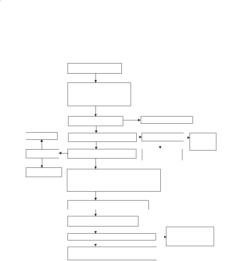
Phone is totally dead
This means that the phone doesn't take current at all when the power switch is pressed or when the watchdog disable pin (X001 pin 11, J111) is grounded. Used battery voltage must be higher than 3.1 V. Otherwise the hardware of CCONT (N100) prevents totally power switch±on.
Phone is totally dead |
|
|
|
|
|
|
||||
|
Yes |
|
|
|
|
|
|
|||
|
|
|
|
|
|
|
||||
|
|
No |
|
|
|
|
|
|
||
|
|
|
|
|
Failure in VBAT line |
|
|
|||
|
|
|
|
|
|
|
||||
J232 VBAT is 3.6 V |
|
|
||||||||
Check L103 |
|
|
||||||||
|
|
|
|
|
|
|
||||
|
Yes |
|
|
|
|
|
|
|||
|
|
No |
|
|
|
|
|
|
||
Voltage at J111 is 3.6V |
Faulty CCONT (N100) |
|
|
|||||||
|
|
|
|
|
||||||
|
|
|
|
|||||||
|
Yes |
|
|
|
|
|
|
|||
|
|
|
|
|
|
|
||||
|
|
|
|
|
No |
No |
|
|||
VBB 2.8 V (R115, C107..) |
Check PWR switch |
|||||||||
VXO 2.8 V (C149..) |
|
|
WDDIS (J111)) is |
|
||||||
|
|
to CCONT line: R341, |
||||||||
|
0V, when PWR switch |
|
|
|||||||
When PWR switch is pressed or |
|
|
|
R118 |
||||||
|
|
|
||||||||
|
is pressed |
|
||||||||
WDDIS is grounded (J111) |
|
|
||||||||
|
|
|
||||||||
|
|
|
|
|
|
|||||
|
Yes |
|
|
Yes |
|
|
||||
|
|
|
|
|
||||||
|
|
|
|
|
|
|
|
|
||
See section ºPower doesn't stay onº |
|
|
|
|
|
|
||||
|
Faulty CCONT (N100) |
|
|
|||||||
|
|
|
|
|
|
|
|
|||
Flash programming doesn't work
The flash programming can be done via panel connector X001 or via dedicated PCB pads. In production, the first programming is done via panel connector. After this, the panel connector is cut away, thus the programming must be done via PCB pads visible through the shield under the battery. The main difference between these is that FLASH programming voltage is produced differently.
In flash programming error cases the flash prommer can give some information about a fault. The fault information messages could be:
±MCU doesn't boot
±Serial clock line failure
±Serial data line failure
±External RAM fault
±Algorithm file or alias ID don't find
±MCU flash Vpp error
Original 08/98 |
Page 7 |

NSE±6 |
PAMS |
Disassembly & Troubleshooting Instructions |
Technical Documentation |
In cases of unsuccesful flash programming there is a possibility to check short circuits between the memories and the MCU (MAD2). It is useful to do this test, when the fault information is: MCU doesn't boot, Serial clock line failure or Serial data line failure. The test procedure is following:
1.Connect testpoint J229 to ground.
2.Switch the power on.
3.If the voltage level in testpoint J225 is 2.8 V (º1º), the interface is OK. If there is a short circuit, the voltage level in testpoint J225 stays low and 32kHz square wave signal can be seen in the lines which are already tested.
It must be remembered that this test can only find short circuits, not open pins. In addition upper data lines (15:8) of flash memory D220 are not included in this test.
CCONT pin 54
MAD pin 38
selftest |
MAD pin 134 ( ExtSysResX)) |
passed |
J225 |
|
Page 8 |
Original 08/98 |
PAMS |
NSE±6 |
|
Technical Documentation |
Disassembly & Troubleshooting Instructions |
|
|
||
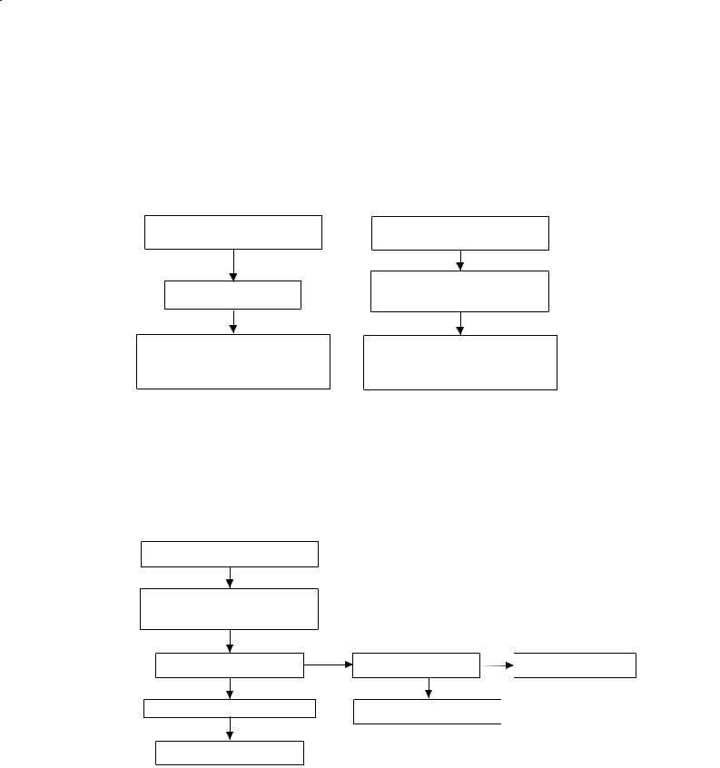
Flash Programming failure (1)
Flash programming doesn't work via panel connector
YES
Check C213, R213
YES
NO
RFC (C664) 13 MHz 800 mV min
NO
Check buffer V660 and VCTCXO G660
If the fault information from prommer is:
a)MCU doesn't boot
b)Serial data line failure
c)Serial clock line failure
connect watchdog disable (WDDIS, J111) line to the ground
OK
NO
VBB (R115, C107 upper side) 2.8 V VXO (C149 upper side ) 2.8 V
YES
J227 master reset (Purx) = º1º (2.8 V)
YES
RfClk (R213 lower side) 13 MHz sine wave
clock signal: 500 mV min
pp
YES
|
See section ºPhone is totally deadº |
|
|||
NO |
|
|
NO |
|
|
|
|
|
|
||
|
J228 sleep clock (SCLK) |
Check sleep |
|||
|
|
|
|
|
|
|
square wave 32 kHz |
||||
|
clock circuitry |
||||
|
|
YES |
|||
|
|
(B101, R154..) |
|||
|
|
|
|
|
|
|
|
|
|
|
|
|
Faulty circuit N100 |
|
|||
|
or overloaded PurX line |
|
|||
Check that following lines are correct: FTX (fbus_tx) line: X001 pin 1 ±±> R215
FRX (fbus_rx) line: X001 pin 2 ±±> R201
FCLK (MBUS) line: X001 pin 3 ±±> R115
Check also pullup and pulldown resistors R115, R201, R215 GND: X001 pin 7 ±±> GND
OK
Enable the selftest function of D200 by connecting
J229 to ground
Connect oscilloscope to testpoint J225 (ExtSysResetX) and switch power on
|
|
NO |
There is a shortcircuit |
Voltage level rises to º1º after power on at testpoint J225 |
|
somewhere in memory control |
|
|
lines or MCU address lines or |
||
|
|
|
|
|
YES |
|
MCU lower (7:0) data lines |
|
|
||
|
|
|
|
There could be open pins in circuits D200 (D220, D240) (open joints may be detectable with microscope)
If not, the PCB or D200 (D220, D240) is faulty.
Original 08/98 |
Page 9 |
NSE±6 |
PAMS |
Disassembly & Troubleshooting Instructions |
Technical Documentation |
Flash Programming failure (2)
Flash programming doesn't work via panel connector
If the fault information is:
External RAM fault
Check control lines of SRAM (D230): RamSelX (J235)..
There could be open joints in SRAM
Flash programming doesn't work via panel connector
If the fault information is: Algorithm file or alias ID don't find, ID is unknown etc.
Check control lines of Flash (D220): ROM1SelX (J234)..
Fault could be open joints in Flash or In upper data lines (15:8)
Flash programming doesn't work via panel connector
If the fault information is:
MCU flash Vpp error
Check connections between X001;10 ±±> R211 upper side
Check components C212, R211
Faulty component D220
Page 10 |
Original 08/98 |
PAMS |
NSE±6 |
|
Technical Documentation |
Disassembly & Troubleshooting Instructions |
|
|
||
Flash Programming failure (3)
Flash programming doesn't work
YES
Check C213, R213
YES
NO
RFC (C664) 13 MHz 800 mV min
NO
Check buffer V660 and VCTCXO G660
If the fault information from prommer is:
a)MCU doesn't boot
b)Serial data line failure
c)Serial clock line failure
connect watchdog disable (WDDIS, J111) line to the ground
|
OK |
|
|
|
|
YES |
|
|
||
|
|
NO |
|
|
|
|
|
|
||
VBB (R115, C107 upper side) 2.8 V |
|
|
VBAT is correct 3.6 V |
|
|
Faulty circuit N100 |
||||
|
|
|
|
|
||||||
|
|
|
|
|||||||
VXO (C149 upper side ) 2.8 V |
|
|
|
|
|
|
|
|
||
|
YES |
NO |
NO |
|||||||
|
||||||||||
|
|
|
|
|
|
|
||||
|
|
|
|
|
J228 sleep clock (SCLK) |
|
|
|||
J227 master reset (Purx) = º1º (2.8 V) |
|
|
|
Check sleep |
||||||
|
|
square wave 32 kHz |
|
|||||||
|
|
|
||||||||
|
|
|
|
|
|
clock circuitry |
||||
|
YES |
|
|
|
YES |
|
||||
|
|
|
|
|
(B101, R154..) |
|||||
|
|
|
|
|
|
|
|
|
|
|
RfClk (R213 lower side) 13 MHz sine wave |
|
|
Faulty circuit N100 |
|
|
|||||
clock signal: 500 mV min |
|
|
|
|
||||||
|
|
or overloaded PurX line |
|
|
||||||
|
pp |
|
|
|
|
|||||
|
YES |
|
|
|
|
|
|
|
|
|
|
|
|
|
|
|
|
|
|
|
|
Check that following lines are correct:
FTX (fbus_tx) line: X001 pin 1 ±±> R215
FRX (fbus_rx) line: X001 pin 2 ±±> R201
FCLK (MBUS) line: X001 pin 3 ±±> R115
Check also pullup and pulldown resistors R115, R201, R215
GND: X001 pin 7 ±±> GND
OK
Enable the selftest function of D200 by connecting testpoint J229 to ground
Connect oscilloscope to testpoint J225
(ExtSysResetX) and switch power on
|
|
NO |
There is a shortcircuit |
|
|
somewhere in memory control |
|
Voltage level rises to º1º after power on at testpoint J225 |
|
||
|
lines or MCU address lines or |
||
|
|
|
|
YES |
MCU lower (7:0) data lines |
|
There could be open pins in circuits D200 (D220, D240) (open joints may be detectable with microscope)
If not, the PCB or D200 (D220, D240) is faulty.
Original 08/98 |
Page 11 |
NSE±6 |
PAMS |
Disassembly & Troubleshooting Instructions |
Technical Documentation |
Flash Programming failure (4)
Flash programming doesn't work
If the fault information is:
External RAM fault
Check control lines of SRAM (D230): RamSelX..
There could be open joints in SRAM
Flash programming doesn't work
YES
If the fault information is:
MCU flash Vpp error
YES
NO
Vpp > 2.8 V (C212)
YES
Check components C212, R211
OK
Faulty component D220
Flash programming doesn't work
If the fault information is:
Algorithm file or alias ID not found,
ID is unknown etc.
Check control lines of Flash (D220):
ROM1SelX (J234)..
Fault could be open joints in Flash or
In upper data lines (15:8)
NO
Vpp > 2.8 V in J221 |
Check regulator N202 |
YES
Check UI connector X303
Page 12 |
Original 08/98 |
Loading...