

DATA SHEET
NPN SILICON RF TWIN TRANSISTOR
µ
PA810TC
NPN SILICON EPITAXIAL TRANSISTOR
(WITH BUILT-IN 2 × 2SC5006)
FLAT-LEAD 6-PIN THIN-TYPE ULTRA SUPER MINIMOLD
DESCRIPTION
The µPA810TC has built-in low-voltage two transistors which are designed to amplify low noise in the VHF band
to the UHF band.
FEATURES
• Low noise: NF = 1.2 dB TYP. @ f = 1 GHz, VCE = 3 V, IC = 7 mA
• High gain: |S21e|2 = 9.0 dB TYP. @ f = 1 GHz, VCE = 3 V, IC = 7 mA
• Flat-lead 6-pin thin-type ultra super minimold
• Built-in 2 transistors (2 × 2SC5006)
ORDERING INFORMATION
Part Number Package Quantity Supplying Form
µ
PA810TC Flat-lead 6-pin Loose products Embossed tape 8 mm wide.
thin-type ultra (50 pcs) Pin 6 (Q1 Base), Pin 5 (Q1 Emitter), Pin 4 (Q2 Emitter) face to
super minimold perforation side of the tape
µ
PA810TC-T1 Taping products
(3 kp/reel)
Remark To order evaluation samples, please contact your local NEC sales office. (Part number for sample order:
µ
PA810TC. Unit sample quantity is 50 pcs.)
.
ABSOLUTE MAXIMUM RATINGS (TA = +25°C)
Parameter Symbol Ratings Unit
Collector to Base Voltage VCBO 20 V
Collector to Emitter Voltage VCEO 12 V
Emitter to Base Voltage VEBO 3V
Collector Current IC 100 mA
Total Power Dissipation PT
Junction Temperature Tj 150 ˚C
Storage Temperature Tstg –65 to +150 ˚C
Note
200 in 1 element mW
230 in 2 elements
Note Mounted on 1.08 cm2 × 1.0 mm glass epoxy substrate.
The information in this document is subject to change without notice. Before using this document, please
confirm that this is the latest version.
Not all devices/types available in every country. Please check with local NEC representative for availability
and additional information.
Document No. P14550EJ1V0DS00 (1st edition)
Date Published November 1999 N CP(K)
Printed in Japan
Caution Electro-static sensitive devices
©
1999
µ
PA810TC
ELECTRICAL CHARACTERISTICS (TA = +25 °C)
Parameter Symbol Conditions MIN. TYP. MAX. Unit
Collector Cutoff Current ICBO VCB = 10 V, IE = 0 – – 1.0
Emitter Cutoff Current IEBO VEB = 1 V, IC = 0 – – 1.0
DC Current Gain hFE VCE = 3 V, IC = 7 mA
Gain Bandwidth Product fT VCE = 3 V, IC = 7 mA, f = 1 GHz 3.0 4.5 – GHz
Feedback Capacitance Cre VCB = 3 V, IE = 0, f = 1 MHz
Insertion Power Gain |S21e|2VCE = 3 V, IC = 7 mA, f = 1 GHz 7.0 9.0 – dB
Noise Figure NF VCE = 3 V, IC = 7 mA, f = 1 GHz – 1.2 2.5 dB
Note 1
Note 2
70 – 140
– 0.7 1.5 pF
Notes 1. Pulse Measurement: PW ≤ 350 µs, Duty Cycle ≤ 2 %
2. Measured with 3-pin bridge, emitter and case should be connected to guard pin of bridge.
hFE CLASSIFICATION
Rank FB
Marking 75
hFE Value 70 to 140
µ
A
µ
A
2 Data Sheet P14550EJ1V0DS00
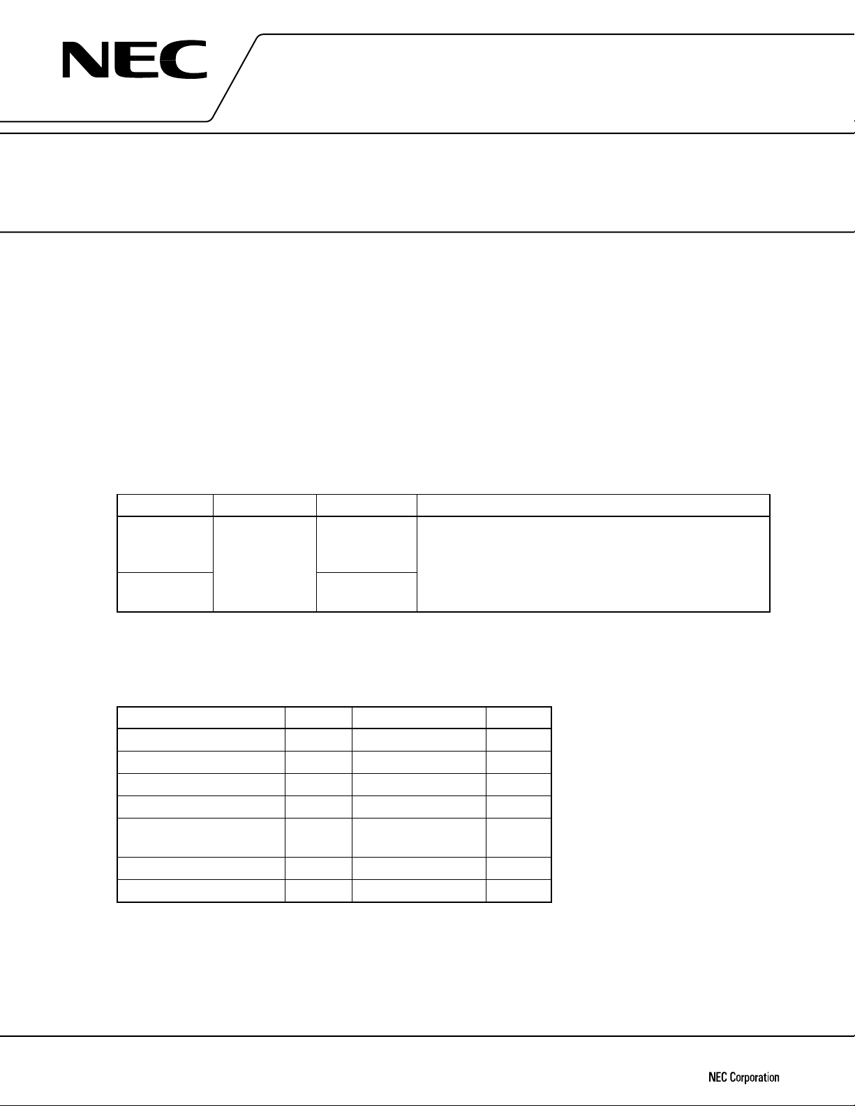
TYPICAL CHARACTERISTICS (TA = +25 °C)
µ
PA810TC
TOTAL POWER DISSIPATION vs.
AMBIENT TEMPERATURE
230
200
(mW)
T
2 Elements in total Free Air
Per
Element
100
Total Power Dissipation P
0
0 50 100 150
Ambient Temperature TA (°C)
COLLECTOR CURRENT vs.
COLLECTOR TO EMITTER VOLTAGE
25
20
(mA)
C
15
IB = 160 A
IB = 140 A
IB = 120 A
10
IB = 100 A
IB = 80 A
5
Collector Current I
IB = 60 A
IB = 40 A
0
0123456
IB = 20 A
Collector to Emitter Voltage VCE (V)
COLLECTOR CURRENT vs. BASE TO
EMITTER VOLTAGE
20
VCE = 3 V
(mA)
C
10
Collector Current I
0
0 0.5 1.0
Base to Emitter Voltage VBE (V)
DC CURRENT GAIN vs.
COLLECTOR CURRENT
1 000
VCE = 3 V
µ
FE
µ
µ
100
µ
µ
µ
DC Current Gain h
µ
µ
10
0.1 1 10 100
Collector Current IC (mA)
GAIN BANDWIDTH PRODUCT vs.
COLLECTOR CURRENT
6.00
VCE = 3 V
f = 1 GHz
5.00
(GHz)
T
4.00
3.00
2.00
1.00
Gain Bandwidth Product f
0.00
1 10 100
Collector Current IC (mA)
INSERTION POWER GAIN vs.
COLLECTOR CURRENT
14.00
VCE = 3 V
f = 1 GHz
12.00
(dB)
2
21e
10.00
8.00
6.00
4.00
Insertion Power Gain S
2.00
1 10 100
Collector Current IC (mA)
Data Sheet P14550EJ1V0DS00 3
µ
PA810TC
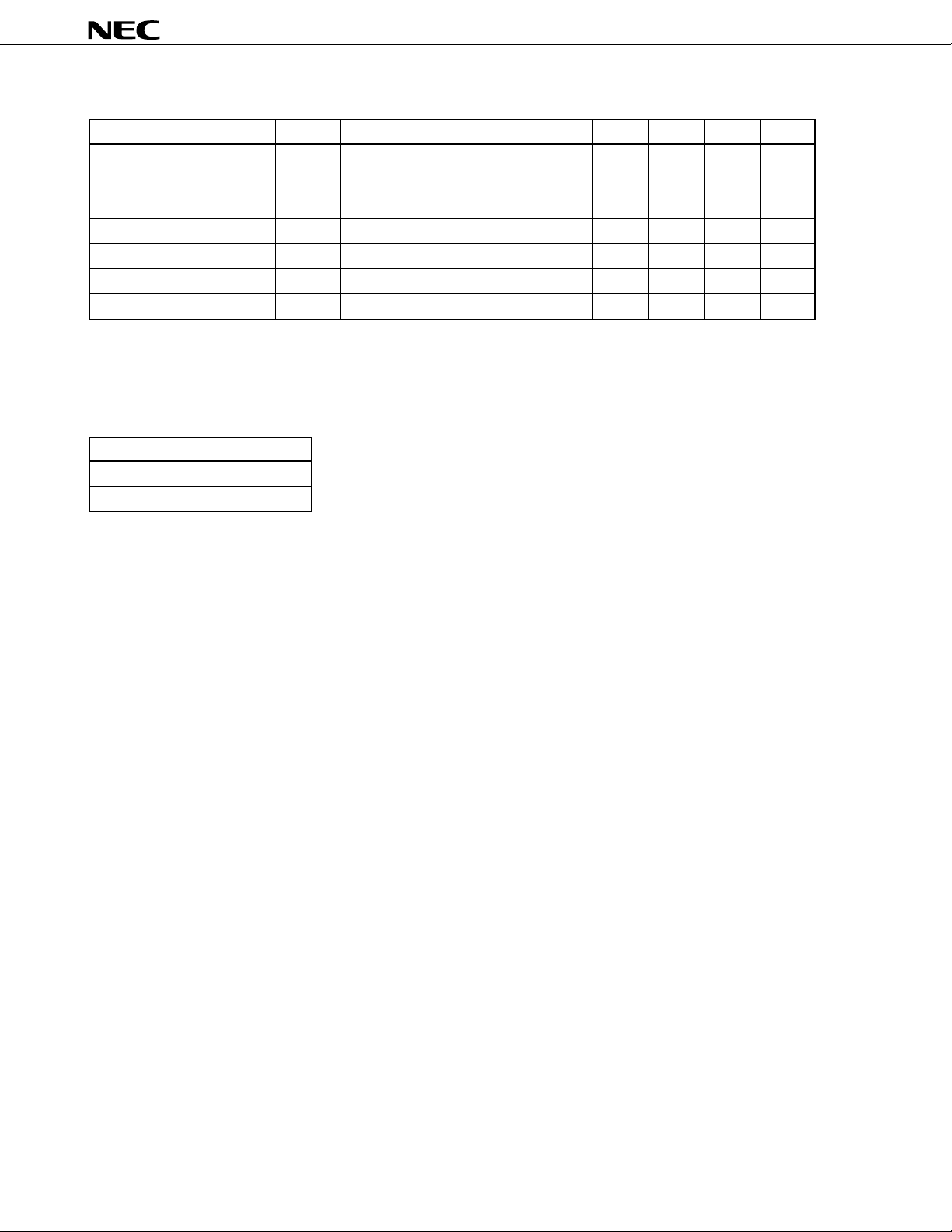
NOISE FIGURE vs. COLLECTOR CURRENT
6.00
VCE = 3 V
f = 1 GHz
5.00
4.00
3.00
2.00
Noise Figure NF (dB)
1.00
0.00
1 10 100
Collector Current IC (mA)
FEEDBACK CAPACITANCE vs.
COLLECTOR TO BASE VOLTAGE
0.900
0.800
(pF)
0.700
re
0.600
0.500
0.400
0.300
0.200
Feedback Capacitance C
0.100
0.000
1 10 100
Collector to Base Voltage VCB (V)
f = 1 MHz
INSERTION POWER GAIN vs. FREQUENCY
25.0
(dB)
2
20.0
21e
15.0
10.0
5.0
Insertion Power Gain S
0.0
0.1 1.0 10.0
Frequency f (GHz)
VCE = 3 V
I
C
= 7 mA
4 Data Sheet P14550EJ1V0DS00

S-PARAMETERS Q1
VCE = 3 V, IC = 1 mA
FREQUENCY S11 S21 S12 S22
GHz MAG. ANG. MAG. ANG. MAG. ANG. MAG. ANG.
0.1 0.949 –30.7 3.885 156.9 0.056 46.5 0.990 –13.3
0.2 0.916 –58.0 3.492 136.7 0.077 53.1 0.942 –26.2
0.3 0.883 –82.5 3.150 118.8 0.107 35.9 0.897 –38.0
0.4 0.835 –106.7 2.819 101.2 0.126 22.2 0.838 –48.3
0.5 0.808 –127.0 2.566 85.6 0.135 7.8 0.786 –57.4
0.6 0.774 –146.3 2.282 71.3 0.145 –2.5 0.747 –65.9
0.7 0.764 –163.4 2.074 57.7 0.155 –13.9 0.713 –73.9
0.8 0.748 –179.2 1.892 45.6 0.153 –24.1 0.684 –82.4
0.9 0.738 165.9 1.730 33.6 0.151 –31.6 0.662 –89.9
1.0 0.729 152.0 1.607 22.3 0.150 –39.8 0.643 –97.9
1.1 0.733 138.9 1.490 11.4 0.146 –48.3 0.625 –106.2
1.2 0.727 126.4 1.394 0.7 0.140 –54.3 0.615 –114.4
1.3 0.733 115.0 1.307 –9.2 0.134 –59.8 0.603 –122.7
1.4 0.732 103.2 1.230 –19.5 0.129 –65.4 0.595 –131.0
1.5 0.737 92.6 1.162 –29.1 0.126 –71.9 0.583 –139.8
1.6 0.739 81.7 1.105 –38.6 0.116 –75.3 0.576 –148.3
1.7 0.744 71.5 1.048 –48.0 0.116 –77.5 0.570 –157.5
1.8 0.746 61.4 1.003 –57.5 0.110 –79.5 0.565 –167.0
1.9 0.752 51.8 0.955 –66.2 0.108 –81.9 0.561 –176.6
2.0 0.752 42.2 0.910 –75.1 0.108 –81.8 0.555 174.3
2.1 0.758 32.8 0.871 –83.6 0.111 –83.7 0.549 164.4
2.2 0.759 23.8 0.832 –92.5 0.112 –82.2 0.545 153.7
2.3 0.767 15.0 0.802 –100.4 0.120 –83.3 0.539 143.2
2.4 0.768 6.0 0.768 –108.8 0.132 –84.4 0.537 132.7
2.5 0.770 –2.3 0.740 –116.5 0.144 –88.2 0.528 121.7
2.6 0.775 –11.0 0.711 –124.6 0.161 –92.7 0.522 110.5
2.7 0.779 –19.0 0.691 –132.1 0.178 –97.7 0.515 99.2
2.8 0.779 –26.7 0.667 –139.8 0.196 –105.0 0.505 88.0
2.9 0.782 –34.4 0.649 –147.6 0.207 –113.2 0.488 77.9
3.0 0.791 –42.1 0.616 –155.5 0.216 –122.8 0.482 69.4
µ
PA810TC
VCE = 3 V, IC = 3 mA
FREQUENCY S11 S21 S12 S22
GHz MAG. ANG. MAG. ANG. MAG. ANG. MAG. ANG.
0.1 0.872 –40.4 9.566 149.6 0.049 43.5 0.952 –20.7
0.2 0.789 –76.2 8.034 126.3 0.068 46.8 0.832 –38.1
0.3 0.735 –105.5 6.761 107.1 0.082 32.8 0.722 –50.9
0.4 0.686 –131.0 5.671 90.2 0.091 19.2 0.630 –61.6
0.5 0.660 –150.8 4.890 75.8 0.098 9.2 0.562 –69.7
0.6 0.636 –169.3 4.198 62.8 0.106 1.4 0.512 –77.2
0.7 0.625 175.0 3.707 51.3 0.107 –7.9 0.476 –83.7
0.8 0.623 160.9 3.325 40.2 0.110 –13.8 0.443 –90.7
0.9 0.617 147.7 2.991 29.8 0.112 –19.4 0.421 –97.9
1.0 0.616 135.7 2.731 19.5 0.111 –24.1 0.400 –104.5
1.1 0.618 123.9 2.513 9.7 0.114 –28.5 0.382 –112.5
1.2 0.614 112.8 2.324 0.2 0.119 –33.8 0.372 –120.0
1.3 0.625 102.4 2.169 –9.2 0.119 –37.1 0.359 –127.7
1.4 0.629 92.2 2.035 –18.3 0.120 –42.1 0.347 –135.5
1.5 0.634 82.5 1.912 –27.3 0.124 –45.3 0.340 –144.2
1.6 0.639 72.6 1.805 –36.6 0.128 –50.3 0.329 –151.8
1.7 0.645 63.5 1.711 –45.3 0.132 –54.1 0.320 –161.2
1.8 0.651 54.2 1.621 –54.3 0.139 –58.5 0.314 –169.5
1.9 0.656 45.4 1.545 –62.8 0.145 –62.5 0.309 –179.4
2.0 0.661 36.5 1.471 –71.5 0.153 –66.8 0.297 172.1
2.1 0.668 27.8 1.409 –79.8 0.156 –72.1 0.293 162.5
2.2 0.672 19.8 1.348 –88.5 0.163 –75.8 0.286 152.4
2.3 0.678 11.3 1.297 –96.7 0.172 –81.3 0.276 141.0
2.4 0.683 2.9 1.243 –105.0 0.183 –86.4 0.274 130.8
2.5 0.691 –4.7 1.202 –113.1 0.194 –92.4 0.268 119.4
2.6 0.698 –12.4 1.158 –121.3 0.208 –98.4 0.263 107.8
2.7 0.701 –19.9 1.111 –129.3 0.218 –104.9 0.258 96.8
2.8 0.714 –27.6 1.067 –137.7 0.231 –113.3 0.255 86.6
2.9 0.722 –34.9 1.026 –145.4 0.233 –121.0 0.248 77.8
3.0 0.736 –42.3 0.983 –152.9 0.234 –129.9 0.261 69.1
Data Sheet P14550EJ1V0DS00 5

VCE = 3 V, IC = 5 mA
FREQUENCY S11 S21 S12 S22
GHz MAG. ANG. MAG. ANG. MAG. ANG. MAG. ANG.
0.1 0.788 –51.6 13.755 144.7 0.031 52.4 0.911 –26.2
0.2 0.712 –90.1 10.866 119.6 0.064 46.6 0.739 –46.1
0.3 0.649 –120.7 8.673 100.1 0.068 30.2 0.607 –59.3
0.4 0.610 –144.4 7.054 84.3 0.078 18.2 0.514 –68.4
0.5 0.596 –164.3 5.936 70.7 0.082 12.2 0.442 –76.0
0.6 0.582 179.5 5.078 58.8 0.090 7.5 0.397 –83.4
0.7 0.571 164.9 4.415 48.0 0.094 –1.4 0.361 –89.4
0.8 0.570 151.3 3.924 37.5 0.098 –6.1 0.335 –95.7
0.9 0.568 139.2 3.531 27.5 0.099 –8.2 0.314 –103.5
1.0 0.574 127.9 3.199 17.9 0.105 –13.6 0.295 –110.0
1.1 0.577 117.2 2.937 8.5 0.113 –18.5 0.280 –117.1
1.2 0.579 106.4 2.708 –0.8 0.118 –24.0 0.265 –124.0
1.3 0.588 96.9 2.523 –9.8 0.120 –28.6 0.258 –132.1
1.4 0.586 86.9 2.353 –18.5 0.127 –32.8 0.246 –140.0
1.5 0.596 77.7 2.210 –27.5 0.131 –37.1 0.237 –148.1
1.6 0.603 68.5 2.079 –36.1 0.139 –43.3 0.225 –156.5
1.7 0.609 59.8 1.974 –44.6 0.148 –47.0 0.219 –166.4
1.8 0.615 50.9 1.872 –53.3 0.154 –51.8 0.210 –174.6
1.9 0.623 42.4 1.779 –61.8 0.160 –58.6 0.202 175.3
2.0 0.626 33.8 1.692 –70.3 0.169 –63.8 0.196 165.5
2.1 0.633 25.4 1.621 –78.7 0.176 –69.2 0.188 155.2
2.2 0.638 17.4 1.548 –87.2 0.184 –75.2 0.181 144.2
2.3 0.648 9.5 1.490 –95.1 0.192 –80.7 0.176 132.7
2.4 0.654 1.5 1.431 –103.4 0.203 –86.9 0.171 120.5
2.5 0.655 –6.1 1.375 –111.0 0.212 –93.4 0.168 108.1
2.6 0.666 –13.8 1.324 –119.4 0.223 –99.8 0.164 96.2
2.7 0.669 –20.8 1.280 –127.2 0.237 –106.9 0.165 84.0
2.8 0.682 –28.3 1.225 –135.5 0.244 –115.0 0.164 73.7
2.9 0.696 –35.4 1.176 –143.2 0.250 –123.5 0.161 65.2
3.0 0.715 –42.9 1.128 –150.7 0.246 –131.7 0.178 56.6
µ
PA810TC
VCE = 3 V, IC = 7 mA
FREQUENCY S11 S21 S12 S22
GHz MAG. ANG. MAG. ANG. MAG. ANG. MAG. ANG.
0.1 0.719 –60.9 18.194 138.9 0.045 46.4 0.866 –32.7
0.2 0.635 –105.8 13.362 112.4 0.051 45.0 0.637 –52.7
0.3 0.579 –134.7 10.199 94.0 0.062 30.2 0.504 –65.7
0.4 0.563 –158.0 8.075 79.1 0.068 23.4 0.414 –74.9
0.5 0.545 –176.3 6.672 66.7 0.074 18.5 0.342 –81.1
0.6 0.538 169.1 5.657 55.5 0.077 13.1 0.312 –87.7
0.7 0.540 155.1 4.904 44.9 0.081 9.9 0.279 –93.2
0.8 0.539 143.2 4.348 35.3 0.087 3.7 0.254 –99.6
0.9 0.543 132.1 3.880 25.6 0.097 –2.0 0.235 –106.7
1.0 0.546 121.6 3.520 16.5 0.105 –5.3 0.220 –113.3
1.1 0.551 111.1 3.225 7.3 0.110 –10.2 0.207 –121.0
1.2 0.554 101.4 2.972 –1.7 0.119 –15.8 0.195 –127.3
1.3 0.561 92.5 2.759 –10.2 0.123 –20.9 0.184 –136.1
1.4 0.564 82.9 2.577 –18.8 0.132 –26.3 0.171 –144.6
1.5 0.575 74.1 2.415 –27.7 0.139 –31.9 0.163 –153.3
1.6 0.582 65.2 2.267 –36.4 0.148 –37.4 0.154 –163.5
1.7 0.588 56.9 2.155 –44.4 0.159 –43.3 0.145 –171.9
1.8 0.594 48.4 2.024 –53.2 0.164 –48.3 0.139 178.9
1.9 0.602 40.2 1.940 –61.3 0.174 –55.2 0.134 166.8
2.0 0.607 31.9 1.838 –69.7 0.182 –60.5 0.125 155.6
2.1 0.616 23.6 1.762 –77.8 0.188 –67.2 0.117 145.2
2.2 0.619 16.0 1.681 –86.2 0.200 –73.3 0.111 129.8
2.3 0.629 8.2 1.616 –94.2 0.207 –79.5 0.110 115.2
2.4 0.633 0.4 1.551 –102.3 0.221 –86.2 0.107 100.7
2.5 0.639 –7.0 1.488 –110.1 0.230 –93.3 0.105 86.1
2.6 0.649 –13.9 1.434 –118.6 0.242 –99.8 0.109 73.3
2.7 0.659 –21.1 1.380 –126.1 0.255 –108.1 0.105 59.7
2.8 0.671 –27.8 1.315 –134.1 0.255 –116.9 0.105 52.2
2.9 0.698 –35.2 1.262 –141.5 0.255 –126.0 0.111 46.6
3.0 0.717 –43.2 1.217 –148.4 0.243 –132.8 0.137 40.2
6 Data Sheet P14550EJ1V0DS00

S-PARAMETERS Q2
VCE = 3 V, IC = 1 mA
FREQUENCY S11 S21 S12 S22
GHz MAG. ANG. MAG. ANG. MAG. ANG. MAG. ANG.
0.1 0.725 –58.0 15.087 138.9 0.039 60.2 0.850 –34.1
0.2 0.618 –99.7 11.136 112.1 0.066 41.7 0.645 –54.8
0.3 0.554 –128.8 8.515 93.3 0.077 31.6 0.508 –68.5
0.4 0.510 –153.2 6.744 78.1 0.088 26.7 0.421 –78.2
0.5 0.488 –170.9 5.601 65.6 0.091 20.7 0.353 –85.5
0.6 0.475 173.4 4.751 53.8 0.106 17.7 0.315 –92.7
0.7 0.471 160.2 4.115 43.5 0.111 10.9 0.288 –99.7
0.8 0.470 147.1 3.661 33.4 0.121 5.4 0.264 –106.4
0.9 0.467 135.4 3.277 23.6 0.130 2.8 0.246 –113.4
1.0 0.467 123.9 2.985 14.3 0.139 –2.9 0.233 –119.4
1.1 0.470 113.7 2.742 5.1 0.151 –8.4 0.219 –127.6
1.2 0.471 103.3 2.536 –4.0 0.161 –13.3 0.214 –134.2
1.3 0.473 94.2 2.365 –12.6 0.170 –18.5 0.207 –141.5
1.4 0.473 84.3 2.223 –21.2 0.181 –23.8 0.199 –148.8
1.5 0.480 75.2 2.088 –30.0 0.193 –30.2 0.195 –157.4
1.6 0.481 66.0 1.984 –38.4 0.204 –36.0 0.189 –165.8
1.7 0.482 57.5 1.885 –46.8 0.217 –40.7 0.188 –174.4
1.8 0.488 48.5 1.796 –55.1 0.228 –47.3 0.180 178.2
1.9 0.489 40.0 1.731 –63.2 0.241 –54.0 0.179 168.5
2.0 0.493 31.3 1.655 –71.6 0.252 –59.7 0.174 160.1
2.1 0.497 22.7 1.598 –79.6 0.263 –66.2 0.168 150.8
2.2 0.500 15.0 1.537 –87.8 0.276 –72.5 0.166 141.5
2.3 0.505 6.7 1.492 –95.5 0.288 –78.6 0.162 130.8
2.4 0.505 –1.6 1.443 –103.5 0.302 –85.2 0.158 121.2
2.5 0.507 –9.7 1.400 –111.1 0.315 –91.6 0.156 110.8
2.6 0.517 –17.6 1.360 –119.4 0.327 –98.1 0.156 99.5
2.7 0.518 –25.6 1.328 –126.7 0.343 –104.6 0.155 88.5
2.8 0.519 –33.5 1.291 –134.2 0.356 –111.8 0.154 78.5
2.9 0.521 –41.5 1.267 –142.0 0.370 –118.3 0.156 67.3
3.0 0.524 –48.6 1.232 –149.3 0.382 –125.4 0.159 57.6
µ
PA810TC
VCE = 3 V, IC = 3 mA
FREQUENCY S11 S21 S12 S22
GHz MAG. ANG. MAG. ANG. MAG. ANG. MAG. ANG.
0.1 0.853 –42.4 8.913 147.9 0.049 45.5 0.949 –24.5
0.2 0.773 –78.7 7.359 123.2 0.083 44.9 0.796 –41.9
0.3 0.695 –108.6 6.081 103.3 0.092 28.0 0.684 –55.5
0.4 0.628 –131.6 5.025 86.5 0.108 18.0 0.593 –66.5
0.5 0.602 –152.3 4.325 72.0 0.112 11.4 0.523 –74.4
0.6 0.576 –170.1 3.701 59.2 0.119 4.5 0.478 –82.8
0.7 0.557 174.3 3.257 47.4 0.122 –1.9 0.442 –90.0
0.8 0.552 160.2 2.905 36.5 0.127 –7.8 0.416 –96.9
0.9 0.545 146.8 2.630 25.8 0.132 –10.4 0.399 –104.3
1.0 0.543 134.7 2.402 15.8 0.132 –15.8 0.380 –111.5
1.1 0.542 123.0 2.215 5.9 0.138 –21.5 0.368 –119.3
1.2 0.540 112.4 2.060 –3.5 0.145 –25.2 0.354 –126.1
1.3 0.543 101.4 1.913 –12.8 0.152 –28.7 0.352 –134.4
1.4 0.546 90.9 1.806 –21.9 0.157 –32.4 0.347 –141.5
1.5 0.550 81.2 1.704 –31.1 0.164 –35.8 0.339 –149.8
1.6 0.549 71.4 1.612 –39.5 0.171 –40.8 0.335 –158.0
1.7 0.553 62.2 1.538 –48.1 0.182 –44.9 0.332 –166.2
1.8 0.557 52.5 1.470 –57.0 0.190 –49.6 0.326 –174.5
1.9 0.559 43.3 1.412 –65.0 0.203 –54.3 0.325 176.3
2.0 0.561 33.9 1.360 –73.7 0.213 –59.6 0.320 168.1
2.1 0.568 25.6 1.303 –81.5 0.224 –65.0 0.315 158.9
2.2 0.567 16.6 1.258 –90.1 0.240 –70.3 0.313 149.6
2.3 0.571 7.9 1.217 –97.8 0.253 –75.8 0.308 140.2
2.4 0.572 –0.6 1.178 –105.9 0.266 –81.6 0.308 130.6
2.5 0.576 –9.2 1.145 –113.6 0.282 –87.6 0.304 120.5
2.6 0.584 –17.7 1.117 –121.5 0.298 –93.7 0.303 110.5
2.7 0.586 –26.1 1.082 –129.0 0.315 –99.8 0.301 100.7
2.8 0.587 –34.2 1.056 –136.8 0.331 –106.5 0.303 90.7
2.9 0.587 –42.4 1.033 –143.9 0.344 –113.0 0.299 80.1
3.0 0.590 –50.4 1.010 –151.3 0.361 –119.5 0.303 70.4
Data Sheet P14550EJ1V0DS00 7

VCE = 3 V, IC = 5 mA
FREQUENCY S11 S21 S12 S22
GHz MAG. ANG. MAG. ANG. MAG. ANG. MAG. ANG.
0.1 0.798 –51.1 12.419 143.0 0.039 25.4 0.905 –31.1
0.2 0.688 –90.5 9.685 116.7 0.071 43.1 0.711 –49.4
0.3 0.613 –120.7 7.637 97.3 0.085 31.9 0.582 –64.1
0.4 0.555 –143.7 6.155 81.4 0.090 22.0 0.482 –74.2
0.5 0.532 –163.5 5.148 68.0 0.101 13.3 0.418 –82.1
0.6 0.516 –179.9 4.399 55.8 0.107 12.7 0.377 –88.9
0.7 0.500 165.1 3.832 45.1 0.110 4.9 0.340 –96.0
0.8 0.499 152.4 3.399 34.6 0.120 1.9 0.317 –103.5
0.9 0.493 139.9 3.066 24.7 0.129 –0.9 0.296 –109.2
1.0 0.493 128.6 2.784 15.0 0.137 –6.9 0.283 –116.5
1.1 0.493 117.5 2.564 5.5 0.144 –12.8 0.272 –124.5
1.2 0.493 107.3 2.377 –3.6 0.153 –16.6 0.263 –130.3
1.3 0.497 97.2 2.217 –12.5 0.160 –22.6 0.256 –138.4
1.4 0.496 87.3 2.078 –21.3 0.172 –26.7 0.248 –146.0
1.5 0.503 77.9 1.966 –30.1 0.184 –32.2 0.244 –153.7
1.6 0.506 68.4 1.856 –38.9 0.194 –37.7 0.238 –162.0
1.7 0.508 59.5 1.767 –47.3 0.205 –42.8 0.237 –171.0
1.8 0.511 50.4 1.687 –55.7 0.215 –48.0 0.232 –178.4
1.9 0.513 41.8 1.623 –63.9 0.227 –54.0 0.223 172.4
2.0 0.515 32.7 1.555 –72.2 0.240 –59.5 0.221 163.5
2.1 0.521 24.3 1.494 –80.2 0.252 –66.1 0.217 155.7
2.2 0.524 16.2 1.445 –88.4 0.264 –71.7 0.213 145.7
2.3 0.526 7.8 1.403 –96.4 0.276 –77.8 0.211 135.9
2.4 0.531 –0.6 1.360 –104.5 0.291 –83.9 0.207 126.3
2.5 0.533 –9.1 1.316 –112.2 0.302 –90.4 0.205 115.9
2.6 0.540 –17.5 1.277 –120.0 0.316 –96.3 0.203 105.5
2.7 0.538 –25.1 1.242 –127.7 0.332 –103.0 0.202 95.6
2.8 0.544 –32.9 1.213 –135.4 0.347 –110.0 0.204 84.8
2.9 0.542 –40.8 1.191 –142.8 0.359 –116.6 0.201 74.2
3.0 0.544 –48.3 1.160 –150.1 0.374 –123.5 0.204 64.2
µ
PA810TC
VCE = 3 V, IC = 7 mA
FREQUENCY S11 S21 S12 S22
GHz MAG. ANG. MAG. ANG. MAG. ANG. MAG. ANG.
0.1 0.725 –58.0 15.087 138.9 0.039 60.2 0.850 –34.1
0.2 0.618 –99.7 11.136 112.1 0.066 41.7 0.645 –54.8
0.3 0.554 –128.8 8.515 93.3 0.077 31.6 0.508 –68.5
0.4 0.510 –153.2 6.744 78.1 0.088 26.7 0.421 –78.2
0.5 0.488 –170.9 5.601 65.6 0.091 20.7 0.353 –85.5
0.6 0.475 173.4 4.751 53.8 0.106 17.7 0.315 –92.7
0.7 0.471 160.2 4.115 43.5 0.111 10.9 0.288 –99.7
0.8 0.470 147.1 3.661 33.4 0.121 5.4 0.264 –106.4
0.9 0.467 135.4 3.277 23.6 0.130 2.8 0.246 –113.4
1.0 0.467 123.9 2.985 14.3 0.139 –2.9 0.233 –119.4
1.1 0.470 113.7 2.742 5.1 0.151 –8.4 0.219 –127.6
1.2 0.471 103.3 2.536 –4.0 0.161 –13.3 0.214 –134.2
1.3 0.473 94.2 2.365 –12.6 0.170 –18.5 0.207 –141.5
1.4 0.473 84.3 2.223 –21.2 0.181 –23.8 0.199 –148.8
1.5 0.480 75.2 2.088 –30.0 0.193 –30.2 0.195 –157.4
1.6 0.481 66.0 1.984 –38.4 0.204 –36.0 0.189 –165.8
1.7 0.482 57.5 1.885 –46.8 0.217 –40.7 0.188 –174.4
1.8 0.488 48.5 1.796 –55.1 0.228 –47.3 0.180 178.2
1.9 0.489 40.0 1.731 –63.2 0.241 –54.0 0.179 168.5
2.0 0.493 31.3 1.655 –71.6 0.252 –59.7 0.174 160.1
2.1 0.497 22.7 1.598 –79.6 0.263 –66.2 0.168 150.8
2.2 0.500 15.0 1.537 –87.8 0.276 –72.5 0.166 141.5
2.3 0.505 6.7 1.492 –95.5 0.288 –78.6 0.162 130.8
2.4 0.505 –1.6 1.443 –103.5 0.302 –85.2 0.158 121.2
2.5 0.507 –9.7 1.400 –111.1 0.315 –91.6 0.156 110.8
2.6 0.517 –17.6 1.360 –119.4 0.327 –98.1 0.156 99.5
2.7 0.518 –25.6 1.328 –126.7 0.343 –104.6 0.155 88.5
2.8 0.519 –33.5 1.291 –134.2 0.356 –111.8 0.154 78.5
2.9 0.521 –41.5 1.267 –142.0 0.370 –118.3 0.156 67.3
3.0 0.524 –48.6 1.232 –149.3 0.382 –125.4 0.159 57.6
8 Data Sheet P14550EJ1V0DS00

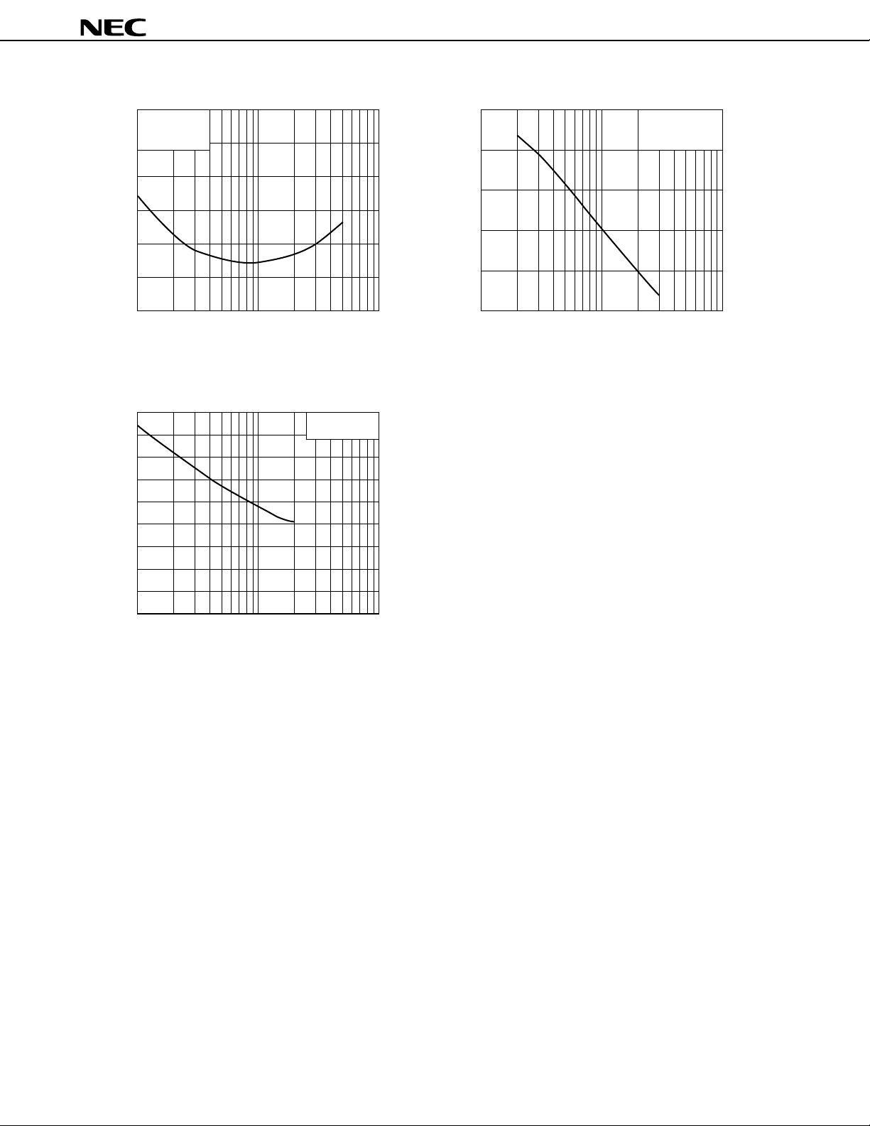
PACKAGE DIMENSIONS
FLAT-LEAD 6 PIN THIN-TYPE ULTRA SUPER MINIMOLD (UNIT: mm)
(Top View)
B1
E1
E2
µ
PA810TC
1.50±0.1
0.96
0.480.48
0.55±0.05
1.50±0.1
1.10±0.1
123
75
+0.1
–0.05
0.20
654
+0.1
–0.05
0.11
PIN CONNECTIONS
1. Collector (Q1)
2. Base (Q2)
3. Collector (Q2)
Q1
C1
6
5
4
Q2
1
2
B2
3
C2
4. Emitter (Q2)
5. Emitter (Q1)
6. Base (Q1)
Data Sheet P14550EJ1V0DS00 9

[MEMO]
µ
PA810TC
10 Data Sheet P14550EJ1V0DS00

[MEMO]
µ
PA810TC
Data Sheet P14550EJ1V0DS00 11

µ
PA810TC
• The information in this document is subject to change without notice. Before using this document, please
confirm that this is the latest version.
• No part of this document may be copied or reproduced in any form or by any means without the prior written
consent of NEC Corporation. NEC Corporation assumes no responsibility for any errors which may appear in
this document.
• NEC Corporation does not assume any liability for infringement of patents, copyrights or other intellectual property
rights of third parties by or arising from use of a device described herein or any other liability arising from use
of such device. No license, either express, implied or otherwise, is granted under any patents, copyrights or other
intellectual property rights of NEC Corporation or others.
• Descriptions of circuits, software, and other related information in this document are provided for illustrative
purposes in semiconductor product operation and application examples. The incorporation of these circuits,
software, and information in the design of the customer's equipment shall be done under the full responsibility
of the customer. NEC Corporation assumes no responsibility for any losses incurred by the customer or third
parties arising from the use of these circuits, software, and information.
• While NEC Corporation has been making continuous effort to enhance the reliability of its semiconductor devices,
the possibility of defects cannot be eliminated entirely. To minimize risks of damage or injury to persons or
property arising from a defect in an NEC semiconductor device, customers must incorporate sufficient safety
measures in its design, such as redundancy, fire-containment, and anti-failure features.
• NEC devices are classified into the following three quality grades:
"Standard", "Special", and "Specific". The Specific quality grade applies only to devices developed based on a
customer designated “quality assurance program“ for a specific application. The recommended applications of
a device depend on its quality grade, as indicated below. Customers must check the quality grade of each device
before using it in a particular application.
Standard: Computers, office equipment, communications equipment, test and measurement equipment,
audio and visual equipment, home electronic appliances, machine tools, personal electronic
equipment and industrial robots
Special: Transportation equipment (automobiles, trains, ships, etc.), traffic control systems, anti-disaster
systems, anti-crime systems, safety equipment and medical equipment (not specifically designed
for life support)
Specific: Aircraft, aerospace equipment, submersible repeaters, nuclear reactor control systems, life
support systems or medical equipment for life support, etc.
The quality grade of NEC devices is "Standard" unless otherwise specified in NEC's Data Sheets or Data Books.
If customers intend to use NEC devices for applications other than those specified for Standard quality grade,
they should contact an NEC sales representative in advance.
M7 98.8
 Loading...