

PRELIMINARY DATA SHEET
SILICON TRANSISTOR
µ
PA809T
MICROWAVE LOW NOISE AMPLIFIER
NPN SILICON EPITAXIAL TRANSISTOR
(WITH BUILT-IN 2 ELEMENTS) MINI MOLD
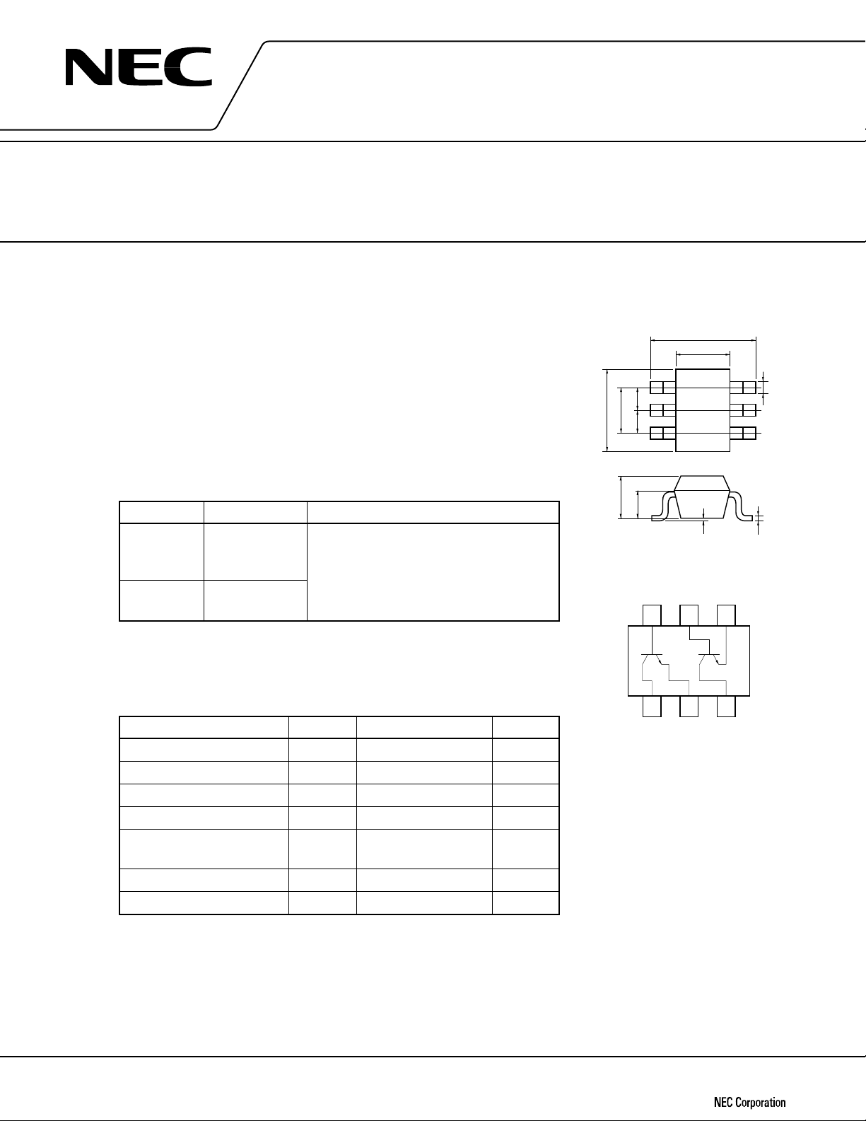
FEATURES PACKAGE DRAWINGS
• Low Voltage Operation, Low Phase Distortion (Unit: mm)
• Low Noise
NF = 1.5 dB TYP. @VCE = 3 V, IC = 7 mA, f = 2 GHz
NF = 1.7 dB TYP. @V
CE = 1 V, IC = 3 mA, f = 2 GHz
• Large Absolute Maximum Collector Current
IC = 100 mA
• A Mini Mold Package Adopted
• Built-in 2 Transistors (2 × 2SC5193)
1.3
2.0±0.2
0.650.65
2.1±0.1
1.25±0.1
123
XY
654
–0
+0.1
0.2
ORDERING INFORMATION
PART NUMBER
µ
PA809T Loose products Embossed tape 8 mm wide. Pin 6 (Q1
µ
PA809T-T1 Taping products
Remark If you require an evaluation sample, please contact an NEC
Sales Representative. (Unit sample quantity is 50 pcs.)
QUANTITY PACKING STYLE
(50 PCS) Base), Pin 5 (Q2 Base), Pin 4 (Q2 Emitter)
face to perforation side of the tape.
(3 KPCS/Reel)
PIN CONFIGURATION (Top View)
ABSOLUTE MAXIMUM RATINGS (TA = 25 °C)
PARAMETER SYMBOL RATING UNIT
Collector to Base Voltage VCBO 9V
Collector to Emitter Voltage VCEO 6V
Emitter to Base Voltage VEBO 2V
Collector Current IC 100 mA
Total Power Dissipation PT 150 in 1 element mW
200 in 2 elements
Junction Temperature Tj 150 ˚C
Storage Temperature Tstg –65 to +150 ˚C
Note
0.7
0.9±0.1
654
1
Q
123
PIN CONNECTIONS
1. Collector (Q1)
2. Emitter (Q1)
3. Collector (Q2)
0~0.1
Q
2
4. Emitter (Q2)
5. Base (Q2)
6. Base (Q1)
+0.1
–0
0.15
Note 110 mW must not be exceeded in 1 element.
This device uses radio frequency technology. Take due precautions to protect it from excessive input levels such as static electricity.
Document No. ID-3643
(O.D. No. ID-9150)
Date Published April 1995 P
Printed in Japan
The information in this document is subject to change without notice.
©
1995
ELECTRICAL CHARACTERISTICS (TA = 25 °C)
PARAMETER SYMBOL CONDITION MIN. TYP. MAX. UNIT
Collector Cutoff Current ICBO VCB = 5 V, IE = 0 0.1
Emitter Cutoff Current IEBO VEB = 1 V, IC = 0 0.1
DC Current Gain hFE VCE = 1 V, IC = 3 mA
Gain Bandwidth Product (1) fT VCE = 1 V, IC = 3 mA, f = 2 GHz 4.0 4.5 GHz
Gain Bandwidth Product (2) fT VCE = 3 V, IC = 20 mA, f = 2 GHz 9.0 GHz
Feed-back Capacitance Cre VCB = 1 V, IE = 0, f = 1 MHz
Insertion Power Gain (1) |S21|
Insertion Power Gain (2) |S21|
Noise Figure (1) NF VCE = 1 V, IC = 3 mA, f = 2 GHz 1.7 2.5 dB
Noise Figure (2) NF VCE = 3 V, IC = 7 mA, f = 2 GHz 1.5 dB
hFE Ratio hFE1/hFE2 VCE = 1 V, IC = 3 mA 0.85
2
VCE = 1 V, IC = 3 mA, f = 2 GHz 2.5 3.5 dB
2
VCE = 3 V, IC = 20 mA, f = 2 GHz 6.5 dB
A smaller value among
hFE of hFE1 = Q1, Q2
A larger value among
hFE of hFE2 = Q1, Q2
Note 1
Note 2
80 160
0.75 0.85 pF
µ
PA809T
µ
A
µ
A
Notes 1. Pulse Measurement: Pw ≤ 350 µs, Duty cycle ≤ 2 %
2. Measured with 3-pin bridge, emitter and case should be connected to guard pin of bridge.
hFE CLASSIFICATION
Rank KB
Marking T88
hFE Value 80 to 160
2
TYPICAL CHARACTERISTICS (TA = 25 °C)
050
Ambient Temperature T
A
(°C)
TOTAL POWER DISSIPATION vs.
AMBIENT TEMPERATURE
Free Air
Total Power Dissipation P
T
(mW)
100 150
100
200
01
2
3
4
5
6
Collector to Emitter Voltage V
CE
(V)
COLLECTOR CURRENT vs.
COLLECTOR TO EMITTER VOLTAGE
Collector Current I
C
(mA)
10
20
30
200 A
µ
180 A
µ
160 A
µ
140 A
µ
120 A
µ
100 A
µ
80 A
µ
60 A
µ
40 A
µ
IB = 20 A
µ
0 0.5
Base to Emitter Voltage V
BE
(V)
COLLECTOR CURRENT vs.
BASE TO EMITTER VOLTAGE
V
CE
= 1 V
Collector Current I
C
(mA)
1
0.01
0.02
0.05
0.1
0.2
0.5
1
2
5
10
20
100
50
0.1 10.2 2 20 5050.5
Collector Current I
C
(mA)
DC Current Gain h
FE
10 100
100
0
200
V
CE
= 1 V
DC CURENT GAIN vs.
COLLECTOR CURRENT
0
Collector Current I
C
(mA)
GAIN BANDWIDTH PRODUCT
vs. COLLECTOR CURRENT
f = 2 GHz
V
CE
= 1 V
Gain Bandwidth Product f
T
(GHz)
35712 10
1357210
5
10
0
5
10
Collector Current I
C
(mA)
INSERTION GAIN vs.
COLLECTOR CURRENT
Insertion Power Gain |S
21e
|
2
(dB)
f = 2 GHz
V
CE
= 1 V
2 Elements in Total
Per Element
µ
PA809T
3

µ
PA809T
3
2
Noise Figure NF (dB)
1
123510
Collector Current lC (mA)
MAXIMUM AVAILABLE GAIN / INSERTION
POWER GAIN vs. FREQUENCY
30
2
l (dB)
21e
20
2
21e
l
IS
NOISE FIGURE vs.
COLLECTOR CURRENT
f = 2 GHz
f = 1 GHz
MAG
VCE = 1 V
7
VCE = 1 V
C
= 5 mA
I
FEED-BACK CAPACITANCE vs.
COLLECTOR TO BASE VOLTAGE
f = 1 MHz
(pF)
re
1.0
0.5
Feed-back Capacitance C
0.1
1520
Collector to Base Voltage V
CB
10
(V)
NOISE FIGURE vs.FREQUENCY
VCE = 1 V
C
= 5 mA
1.5
I
1
10
0
Maximum Available Power Gain MAG (dB)
Insertion Power Gain IS
0.1 0.5 1 5
Frequency f (GHz)
Noise Figure NF (dB)
0.5
0.1 0.5 2
1.0
Frequency f (GHz)
4

S-PARAMETERS
VCE = 1 V, IC = 1 mA, ZO = 50 Ω
FREQUENCY S11 S21 S12 S22
MHz MAG ANG MAG ANG MAG ANG MAG ANG
100.00 0.952 –18.2 3.497 166.0 0.050 74.0 0.979 –8.3
200.00 0.913 –37.9 3.208 150.4 0.101 64.5 0.927 –18.9
300.00 0.871 –55.6 3.048 135.4 0.141 56.5 0.855 –28.2
400.00 0.817 –68.8 2.825 124.1 0.169 49.8 0.803 –33.7
500.00 0.737 –82.6 2.332 114.8 0.184 42.1 0.746 –39.1
600.00 0.657 –93.4 2.236 107.2 0.196 37.7 0.691 –41.0
700.00 0.624 –103.9 2.043 99.0 0.206 33.0 0.639 –45.4
800.00 0.594 –117.9 1.864 91.9 0.208 30.5 0.573 –46.2
900.00 0.560 –127.1 1.715 85.0 0.208 29.0 0.538 –49.5
1000.00 0.544 –137.0 1.593 80.3 0.203 27.8 0.494 –51.7
1100.00 0.527 –145.1 1.458 75.3 0.200 25.6 0.478 –55.7
1200.00 0.534 –154.5 1.391 70.9 0.195 24.4 0.450 –60.1
1300.00 0.554 –163.9 1.258 66.7 0.195 24.1 0.426 –62.4
1400.00 0.566 –169.0 1.200 63.5 0.194 25.6 0.409 –66.3
1500.00 0.547 –175.2 1.185 55.1 0.199 26.0 0.406 –67.7
1600.00 0.523 179.3 1.176 51.3 0.201 29.6 0.392 –72.4
1700.00 0.540 172.6 1.129 48.8 0.198 33.0 0.375 –76.0
1800.00 0.530 165.2 1.109 47.4 0.199 37.3 0.370 –80.9
1900.00 0.559 160.8 1.028 45.2 0.200 40.0 0.365 –87.1
2000.00 0.571 156.2 0.981 43.6 0.203 43.2 0.364 –91.0
VCE = 1 V, IC = 3 mA, ZO = 50 Ω
µ
PA809T
FREQUENCY S11 S21 S12 S22
MHz MAG ANG MAG ANG MAG ANG MAG ANG
100.00 0.864 –29.3 8.784 157.7 0.050 64.3 0.927 –16.5
200.00 0.768 –37.8 7.364 136.9 0.088 56.8 0.797 –34.0
300.00 0.675 –79.1 6.372 139.7 0.115 51.1 0.667 –46.3
400.00 0.584 –94.9 5.374 110.1 0.130 47.2 0.568 –52.1
500.00 0.504 –110.1 4.501 102.3 0.138 44.1 0.485 –55.8
600.00 0.455 –123.0 3.906 96.2 0.148 43.4 0.430 –57.0
700.00 0.428 –134.7 3.298 89.7 0.156 42.3 0.380 –61.3
800.00 0.405 –145.9 2.938 84.1 0.163 42.8 0.321 –63.1
900.00 0.381 –154.2 2.915 79.4 0.171 43.7 0.286 –64.8
1000.00 0.379 –163.1 2.397 75.8 0.178 44.6 0.239 –66.7
1100.00 0.374 –171.9 2.196 72.0 0.184 44.7 0.246 –70.8
1200.00 0.389 –178.5 2.061 68.3 0.190 44.6 0.226 –76.4
1300.00 0.404 174.9 1.916 64.3 0.198 44.2 0.201 –79.4
1400.00 0.414 172.1 1.829 60.6 0.210 44.4 0.184 –83.7
1500.00 0.411 165.7 1.759 55.5 0.225 44.2 0.176 –85.9
1600.00 0.402 161.8 1.680 52.5 0.241 45.3 0.167 –92.5
1700.00 0.417 156.7 1.606 50.1 0.249 48.9 0.159 –97.7
1800.00 0.428 151.2 1.537 49.4 0.259 48.8 0.151 –107.2
1900.00 0.446 148.4 1.458 47.4 0.265 48.7 0.130 –114.4
2000.00 0.457 144.8 1.394 43.8 0.272 48.6 0.155 –120.7
VCE = 1 V, IC = 5 mA, ZO = 50 Ω
FREQUENCY S11 S21 S12 S22
MHz MAG ANG MAG ANG MAG ANG MAG ANG
100.00 0.790 –37.9 12.042 152.3 0.043 67.5 0.886 –23.5
200.00 0.672 –69.2 9.515 129.2 0.079 54.7 0.708 –42.2
300.00 0.564 –91.9 7.780 113.6 0.101 51.0 0.562 –55.7
400.00 0.475 –108.5 3.993 103.8 0.115 49.2 0.456 –61.2
500.00 0.415 –123.8 4.959 97.3 0.124 48.6 0.374 –63.8
600.00 0.383 –137.1 4.268 92.1 0.135 49.0 0.329 –64.4
700.00 0.366 –147.8 3.741 86.2 0.146 48.6 0.289 –69.8
800.00 0.331 –138.3 3.313 81.3 0.156 47.4 0.235 –73.5
900.00 0.332 –166.3 2.927 77.3 0.168 50.2 0.202 –75.2
1000.00 0.335 –174.3 2.677 74.1 0.179 51.1 0.181 –76.6
1100.00 0.337 177.3 2.431 70.7 0.188 50.8 0.175 –81.8
1200.00 0.333 172.0 2.282 67.4 0.197 50.3 0.158 –90.1
1300.00 0.365 166.3 2.124 63.6 0.208 49.5 0.134 –95.4
1400.00 0.375 164.2 2.027 59.9 0.222 48.9 0.120 –101.8
1500.00 0.378 158.6 1.944 55.4 0.240 48.1 0.114 –106.3
1600.00 0.373 155.0 1.850 52.7 0.258 48.4 0.112 –116.2
1700.00 0.387 150.8 1.764 50.6 0.269 49.5 0.107 –128.3
1800.00 0.401 146.1 1.679 50.0 0.279 50.2 0.109 –137.3
1900.00 0.418 143.8 1.603 48.2 0.286 50.1 0.114 –144.5
2000.00 0.429 140.6 1.526 46.7 0.294 49.5 0.125 –150.2
5

VCE = 1 V, IC = 7 mA, ZO = 50 Ω
FREQUENCY S11 S21 S12 S22
MHz MAG ANG MAG ANG MAG ANG MAG ANG
100.00 0.736 –44.1 14.388 148.1 0.041 61.2 0.833 –28.2
200.00 0.603 –77.3 10.890 124.2 0.074 53.6 0.642 –48.4
300.00 0.494 –100.6 8.181 109.3 0.094 51.9 0.497 –62.1
400.00 0.415 –117.8 6.500 100.3 0.108 51.7 0.389 –68.0
500.00 0.369 –133.0 5.307 94.7 0.118 52.1 0.310 –70.2
600.00 0.350 –145.9 4.558 89.8 0.132 52.9 0.271 –70.5
700.00 0.336 –155.9 3.974 84.3 0.144 52.7 0.240 –77.0
800.00 0.324 –166.0 3.500 79.9 0.156 53.1 0.191 –83.3
900.00 0.309 –173.7 3.096 76.3 0.169 53.8 0.158 –85.9
1000.00 0.314 178.7 2.819 73.3 0.183 54.2 0.141 –87.1
1100.00 0.319 171.0 2.583 70.1 0.193 53.7 0.139 –93.2
1200.00 0.335 166.5 2.407 66.9 0.204 52.9 0.128 –104.6
1300.00 0.347 161.6 2.235 63.3 0.215 51.8 0.106 –113.9
1400.00 0.336 159.6 2.137 59.8 0.231 50.8 0.093 –123.2
1500.00 0.362 154.5 2.032 55.5 0.250 49.7 0.093 –129.3
1600.00 0.359 151.2 1.932 52.9 0.268 49.5 0.098 –140.1
1700.00 0.373 147.4 1.845 50.9 0.280 50.4 0.102 –133.9
1800.00 0.388 143.2 1.756 50.5 0.291 50.7 0.110 –161.6
1900.00 0.404 141.0 1.676 48.7 0.299 50.5 0.116 –167.2
2000.00 0.415 138.1 1.597 47.5 0.307 49.6 0.130 –170.3
VCE = 1 V, IC = 10 mA, ZO = 50 Ω
FREQUENCY S11 S21 S12 S22
MHz MAG ANG MAG ANG MAG ANG MAG ANG
100.00 0.676 –49.5 16.485 144.1 0.041 59.8 0.808 –31.3
200.00 0.545 –83.0 11.960 120.0 0.071 53.3 0.588 –53.4
300.00 0.442 –108.8 8.726 105.9 0.090 53.3 0.443 –67.7
400.00 0.372 –126.4 6.820 97.6 0.103 54.1 0.339 –73.9
500.00 0.339 –141.2 5.333 92.6 0.116 54.9 0.263 –76.2
600.00 0.328 –153.6 4.754 88.1 0.130 33.9 0.229 –76.4
700.00 0.318 –162.8 4.124 82.9 0.143 55.4 0.205 –84.2
800.00 0.309 –172.4 3.626 78.7 0.157 55.7 0.162 –93.2
900.00 0.295 –179.8 3.201 75.3 0.171 56.3 0.131 –97.4
1000.00 0.303 173.2 2.922 72.6 0.186 56.4 0.115 –99.3
1100.00 0.310 166.1 2.674 69.6 0.198 55.7 0.118 –105.7
1200.00 0.326 162.2 2.480 66.5 0.209 54.5 0.113 –119.6
1300.00 0.336 157.7 2.312 63.1 0.221 53.1 0.096 –132.9
1400.00 0.345 156.0 2.205 39.5 0.237 51.9 0.089 –144.2
1500.00 0.333 151.3 2.100 55.5 0.257 50.6 0.091 –151.0
1600.00 0.351 148.1 1.989 55.0 0.276 50.2 0.101 –159.3
1700.00 0.360 144.8 1.904 51.0 0.230 50.9 0.111 –171.4
1800.00 0.380 140.9 1.804 50.7 0.300 51.0 0.122 –177.0
1900.00 0.396 139.0 1.724 49.0 0.307 50.7 0.129 178.5
2000.00 0.407 136.0 1.642 47.6 0.315 49.7 0.143 177.0
µ
PA809T
VCE = 3 V, IC = 1 mA, ZO = 50 Ω
FREQUENCY S11 S21 S12 S22
MHz MAG ANG MAG ANG MAG ANG MAG ANG
100.00 1.003 –16.7 3.418 166.9 0.029 74.7 0.989 –3.6
200.00 0.956 –32.7 3.121 154.7 0.078 64.7 0.951 –14.1
300.00 0.938 –48.4 3.082 141.4 0.113 60.2 0.897 –21.7
400.00 0.895 –61.8 2.931 129.6 0.138 53.4 0.857 –26.1
500.00 0.793 –75.1 2.631 120.5 0.130 46.1 0.811 –30.5
600.00 0.700 –83.7 2.365 114.3 0.160 42.9 0.774 –31.5
700.00 0.671 –96.0 2.189 106.3 0.171 38.2 0.735 –35.8
800.00 0.629 –108.8 1.997 98.9 0.172 34.9 0.665 –35.9
900.00 0.581 –117.9 1.837 92.0 0.172 33.9 0.636 –38.4
1000.00 0.554 –127.4 1.706 87.7 0.170 33.3 0.590 –39.3
1100.00 0.535 –135.4 1.570 82.7 0.167 31.4 0.579 –43.2
1200.00 0.531 –145.8 1.510 78.0 0.162 30.6 0.541 –47.1
1300.00 0.540 –156.4 1.359 74.3 0.162 30.5 0.522 –48.3
1400.00 0.542 –161.9 1.299 71.7 0.162 32.5 0.510 –51.5
1500.00 0.527 –168.3 1.278 62.8 0.166 33.5 0.509 –52.6
1600.00 0.497 –174.3 1.272 58.3 0.169 37.6 0.493 –56.2
1700.00 0.512 178.3 1.216 55.8 0.169 41.3 0.476 –58.1
1800.00 0.492 170.4 1.209 54.2 0.171 46.9 0.469 –62.0
1900.00 0.524 165.5 1.119 52.2 0.176 49.9 0.454 –66.3
2000.00 0.534 159.9 1.069 50.4 0.180 33.4 0.454 –69.3
6

VCE = 3 V, IC = 3 mA, ZO = 50 Ω
FREQUENCY S11 S21 S12 S22
MHz MAG ANG MAG ANG MAG ANG MAG ANG
100.00 0.924 –23.0 8.393 160.8 0.031 54.9 0.965 –10.7
200.00 0.830 –46.1 7.259 143.7 0.070 59.2 0.964 –24.0
300.00 0.750 –65.0 6.624 128.1 0.096 55.7 0.760 –34.3
400.00 0.653 –79.4 3.805 116.8 0.111 51.5 0.671 –38.9
500.00 0.548 –93.1 4.720 108.8 0.119 48.5 0.599 –41.3
600.00 0.471 –104.2 4.121 103.1 0.127 47.9 0.555 –41.1
700.00 0.433 –116.2 3.695 96.4 0.136 46.5 0.509 –44.9
800.00 0.397 –128.3 3.302 90.5 0.141 46.3 0.441 –44.6
900.00 0.361 –136.7 2.944 85.5 0.147 47.4 0.409 –43.0
1000.00 0.345 –146.1 2.696 82.0 0.153 48.6 0.378 –44.9
1100.00 0.332 –155.5 2.479 77.9 0.158 48.6 0.368 –48.3
1200.00 0.336 –164.1 2.328 74.3 0.163 48.8 0.338 –52.4
1300.00 0.346 –172.7 2.158 70.3 0.170 48.7 0.314 –52.7
1400.00 0.332 –177.1 2.063 67.1 0.180 49.3 0.300 –54.5
1500.00 0.347 176.5 1.997 61.8 0.194 49.2 0.294 –55.3
1600.00 0.338 171.8 1.906 58.4 0.207 50.6 0.282 –58.8
1700.00 0.349 165.6 1.818 56.0 0.216 52.3 0.262 –60.8
1800.00 0.355 139.2 1.740 55.1 0.225 54.4 0.251 –64.3
1900.00 0.373 155.6 1.650 53.2 0.233 53.1 0.241 –68.3
2000.00 0.387 131.2 1.376 31.6 0.240 55.5 0.239 –72.5
VCE = 3 V, IC = 5 mA, ZO = 50 Ω
FREQUENCY S11 S21 S12 S22
MHz MAG ANG MAG ANG MAG ANG MAG ANG
100.00 0.865 –27.8 11.588 156.9 0.036 49.9 0.938 –13.2
200.00 0.742 –53.4 9.364 137.4 0.066 58.5 0.805 –29.3
300.00 0.637 –73.2 8.312 121.7 0.086 53.0 0.675 –40.3
400.00 0.531 –87.6 6.607 110.7 0.100 53.2 0.576 –44.3
500.00 0.438 –101.3 5.519 103.7 0.109 52.0 0.500 –45.6
600.00 0.376 –113.3 4.799 98.6 0.118 52.5 0.461 –44.5
700.00 0.343 –125.0 4.262 92.5 0.128 52.0 0.418 –48.1
800.00 0.315 –136.9 3.784 87.3 0.135 52.5 0.357 –47.9
900.00 0.286 –145.5 3.354 83.0 0.143 53.5 0.325 –47.4
1000.00 0.276 –154.9 3.048 79.8 0.154 54.4 0.301 –46.6
1100.00 0.268 –164.6 2.812 76.3 0.163 54.4 0.294 –50.1
1200.00 0.276 –172.4 2.613 73.0 0.170 54.2 0.267 –54.7
1300.00 0.286 179.9 2.441 69.4 0.180 53.6 0.243 –54.8
1400.00 0.293 173.9 2.321 63.9 0.192 53.4 0.228 –56.1
1500.00 0.294 169.9 2.232 61.4 0.207 52.8 0.222 –57.0
1600.00 0.290 165.5 2.123 58.3 0.223 53.4 0.211 –61.0
1700.00 0.303 160.1 2.030 56.3 0.234 54.4 0.191 –63.5
1800.00 0.313 154.3 1.932 53.6 0.244 55.8 0.179 –67.5
1900.00 0.330 151.2 1.836 53.8 0.252 56.0 0.171 –71.9
2000.00 0.341 147.2 1.757 52.4 0.259 55.8 0.168 –77.4
µ
PA809T
VCE = 3 V, IC = 7 mA, ZO = 50 Ω
FREQUENCY S11 S21 S12 S22
MHz MAG ANG MAG ANG MAG ANG MAG ANG
100.00 0.811 –32.6 14.032 153.7 0.027 57.0 0.922 –18.2
200.00 0.668 –59.1 11.239 132.2 0.063 56.7 0.752 –33.9
300.00 0.553 –79.0 8.969 116.7 0.081 55.4 0.611 –44.6
400.00 0.449 –93.3 7.293 106.9 0.094 55.4 0.510 –47.9
500.00 0.370 –107.1 6.039 100.6 0.103 55.3 0.435 –48.1
600.00 0.318 –119.6 5.212 93.8 0.114 56.2 0.400 –46.5
700.00 0.290 –131.1 4.581 90.2 0.125 55.8 0.364 –50.1
800.00 0.268 –142.9 4.057 85.5 0.134 56.2 0.305 –50.1
900.00 0.244 –151.8 3.587 81.6 0.145 57.1 0.275 –49.0
1000.00 0.237 –161.2 3.266 78.6 0.157 57.6 0.255 –47.7
1100.00 0.233 –170.9 3.003 75.4 0.167 57.5 0.249 –51.5
1200.00 0.243 –178.1 2.794 72.3 0.173 57.0 0.225 –56.7
1300.00 0.253 174.8 2.596 68.9 0.186 56.1 0.199 –56.7
1400.00 0.261 171.0 2.474 65.4 0.199 55.4 0.185 –37.7
1500.00 0.265 165.4 2.365 61.3 0.216 54.6 0.179 –38.7
1600.00 0.265 161.2 2.253 58.4 0.232 54.7 0.169 –63.3
1700.00 0.277 156.4 2.153 56.5 0.245 55.5 0.149 –66.8
1800.00 0.290 151.1 2.046 56.9 0.233 56.4 0.137 –71.3
1900.00 0.306 148.3 1.943 54.2 0.264 56.4 0.130 –76.7
2000.00 0.318 144.6 1.856 52.8 0.271 53.9 0.128 –83.6
7

VCE = 3 V, IC = 10 mA, ZO = 50 Ω
FREQUENCY S11 S21 S12 S22
MHz MAG ANG MAG ANG MAG ANG MAG ANG
100.00 0.775 –34.3 16.213 130.4 0.031 42.4 0.916 –18.1
200.00 0.609 –63.8 12.257 128.4 0.037 55.3 0.712 –37.2
300.00 0.488 –83.7 9.683 115.4 0.077 56.3 0.569 –47.6
400.00 0.390 –98.0 7.790 104.3 0.091 56.6 0.467 –30.5
500.00 0.321 –111.7 6.396 98.4 0.101 57.6 0.394 –50.4
600.00 0.277 –124.8 5.493 93.8 0.113 58.5 0.362 –48.1
700.00 0.253 –136.0 4.808 88.6 0.125 58.4 0.329 –51.9
800.00 0.236 –147.8 4.252 84.3 0.135 58.4 0.273 –52.2
900.00 0.216 –157.0 3.752 80.7 0.147 59.1 0.242 –50.9
1000.00 0.212 –166.4 3.408 77.8 0.160 59.6 0.224 –49.1
1100.00 0.221 –176.0 3.131 74.8 0.171 59.2 0.220 –53.1
1200.00 0.221 177.3 2.909 71.9 0.180 58.5 0.197 –59.1
1300.00 0.232 170.6 2.711 68.6 0.191 57.3 0.171 –59.2
1400.00 0.240 167.1 2.581 65.2 0.205 56.3 0.157 –60.1
1500.00 0.247 161.8 2.457 61.2 0.222 55.2 0.150 –61.2
1600.00 0.248 158.0 2.335 58.5 0.239 55.2 0.141 –66.8
1700.00 0.261 153.6 2.236 56.6 0.252 53.8 0.121 –71.4
1800.00 0.275 148.5 2.120 56.2 0.263 56.5 0.101 –77.2
1900.00 0.291 146.1 2.019 54.6 0.272 56.4 0.104 –83.3
2000.00 0.302 142.6 1.923 53.2 0.279 56.8 0.104 –91.6
µ
PA809T
8

[MEMO]
µ
PA809T
9

µ
PA809T
No part of this document may be copied or reproduced in any form or by any means without the prior written
consent of NEC Corporation. NEC Corporation assumes no responsibility for any errors which may appear in this
document.
NEC Corporation does not assume any liability for infringement of patents, copyrights or other intellectual
property rights of third parties by or arising from use of a device described herein or any other liability arising
from use of such device. No license, either express, implied or otherwise, is granted under any patents,
copyrights or other intellectual property rights of NEC Corporation or others.
While NEC Corporation has been making continuous effort to enhance the reliability of its semiconductor devices,
the possibility of defects cannot be eliminated entirely. To minimize risks of damage or injury to persons or
property arising from a defect in an NEC semiconductor device, customer must incorporate sufficient safety
measures in its design, such as redundancy, fire-containment, and anti-failure features.
NEC devices are classified into the following three quality grades:
“Standard“, “Special“, and “Specific“. The Specific quality grade applies only to devices developed based on
a customer designated “quality assurance program“ for a specific application. The recommended applications
of a device depend on its quality grade, as indicated below. Customers must check the quality grade of each
device before using it in a particular application.
Standard: Computers, office equipment, communications equipment, test and measurement equipment,
audio and visual equipment, home electronic appliances, machine tools, personal electronic
equipment and industrial robots
Special: Transportation equipment (automobiles, trains, ships, etc.), traffic control systems, anti-disaster
systems, anti-crime systems, safety equipment and medical equipment (not specifically designed
for life support)
Specific: Aircrafts, aerospace equipment, submersible repeaters, nuclear reactor control systems, life
support systems or medical equipment for life support, etc.
The quality grade of NEC devices in “Standard“ unless otherwise specified in NEC's Data Sheets or Data Books.
If customers intend to use NEC devices for applications other than those specified for Standard quality grade,
they should contact NEC Sales Representative in advance.
Anti-radioactive design is not implemented in this product.
10
M4 94.11
 Loading...