DATA SHEET
NPN SILICON RF TWIN TRANSISTOR
µ
PA810TC
NPN SILICON EPITAXIAL TRANSISTOR
(WITH BUILT-IN 2 × 2SC5006)
FLAT-LEAD 6-PIN THIN-TYPE ULTRA SUPER MINIMOLD
DESCRIPTION
The µPA810TC has built-in low-voltage two transistors which are designed to amplify low noise in the VHF band
to the UHF band.
FEATURES
• Low noise: NF = 1.2 dB TYP. @ f = 1 GHz, VCE = 3 V, IC = 7 mA
• High gain: |S21e|2 = 9.0 dB TYP. @ f = 1 GHz, VCE = 3 V, IC = 7 mA
• Flat-lead 6-pin thin-type ultra super minimold
• Built-in 2 transistors (2 × 2SC5006)
ORDERING INFORMATION
Part Number Package Quantity Supplying Form
µ
PA810TC Flat-lead 6-pin Loose products Embossed tape 8 mm wide.
thin-type ultra (50 pcs) Pin 6 (Q1 Base), Pin 5 (Q1 Emitter), Pin 4 (Q2 Emitter) face to
super minimold perforation side of the tape
µ
PA810TC-T1 Taping products
(3 kp/reel)
Remark To order evaluation samples, please contact your local NEC sales office. (Part number for sample order:
µ
PA810TC. Unit sample quantity is 50 pcs.)
.
ABSOLUTE MAXIMUM RATINGS (TA = +25°C)
Parameter Symbol Ratings Unit
Collector to Base Voltage VCBO 20 V
Collector to Emitter Voltage VCEO 12 V
Emitter to Base Voltage VEBO 3V
Collector Current IC 100 mA
Total Power Dissipation PT
Junction Temperature Tj 150 ˚C
Storage Temperature Tstg –65 to +150 ˚C
Note
200 in 1 element mW
230 in 2 elements
Note Mounted on 1.08 cm2 × 1.0 mm glass epoxy substrate.
The information in this document is subject to change without notice. Before using this document, please
confirm that this is the latest version.
Not all devices/types available in every country. Please check with local NEC representative for availability
and additional information.
Document No. P14550EJ1V0DS00 (1st edition)
Date Published November 1999 N CP(K)
Printed in Japan
Caution Electro-static sensitive devices
©
1999

µ
PA810TC
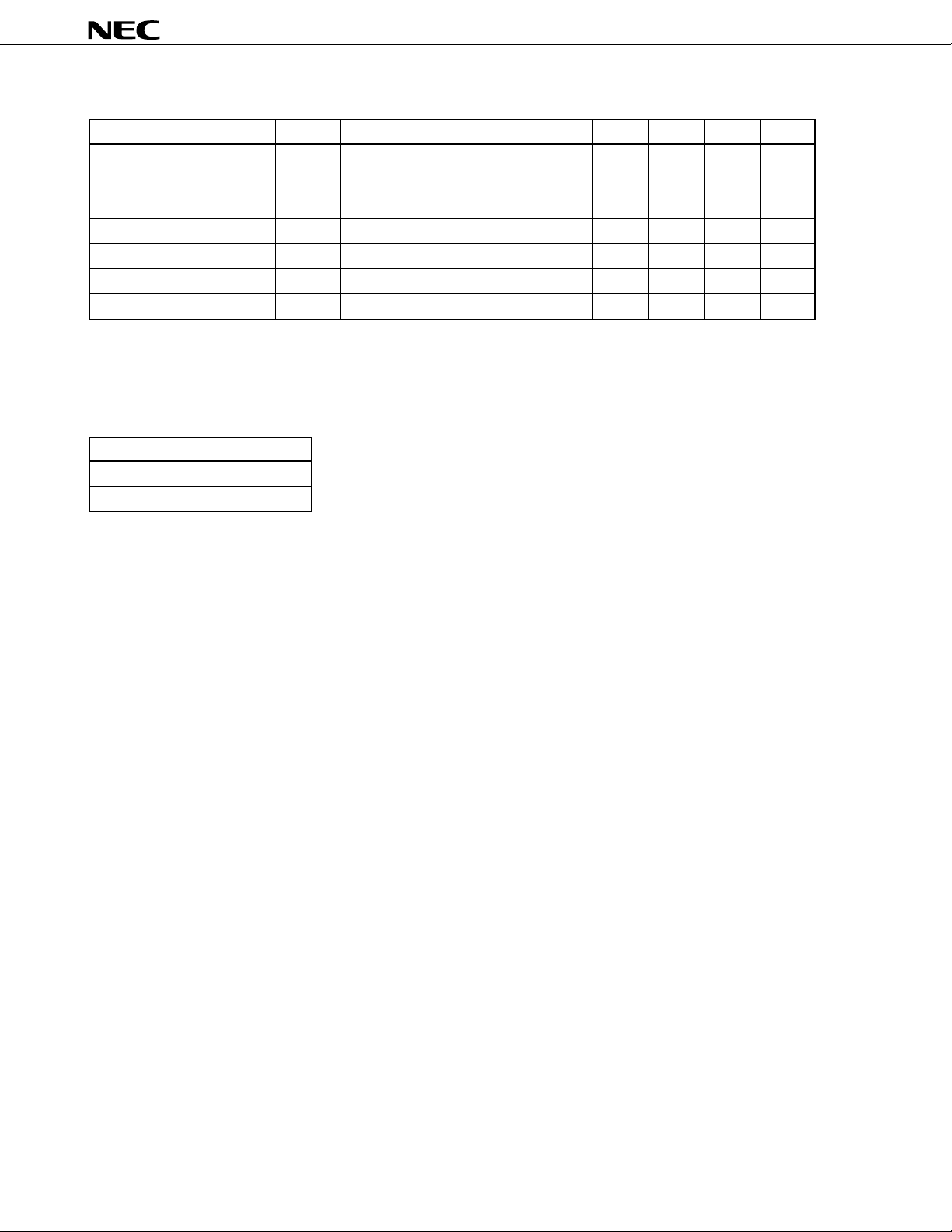
ELECTRICAL CHARACTERISTICS (TA = +25 °C)
Parameter Symbol Conditions MIN. TYP. MAX. Unit
Collector Cutoff Current ICBO VCB = 10 V, IE = 0 – – 1.0
Emitter Cutoff Current IEBO VEB = 1 V, IC = 0 – – 1.0
DC Current Gain hFE VCE = 3 V, IC = 7 mA
Gain Bandwidth Product fT VCE = 3 V, IC = 7 mA, f = 1 GHz 3.0 4.5 – GHz
Feedback Capacitance Cre VCB = 3 V, IE = 0, f = 1 MHz
Insertion Power Gain |S21e|2VCE = 3 V, IC = 7 mA, f = 1 GHz 7.0 9.0 – dB
Noise Figure NF VCE = 3 V, IC = 7 mA, f = 1 GHz – 1.2 2.5 dB
Note 1
Note 2
70 – 140
– 0.7 1.5 pF
Notes 1. Pulse Measurement: PW ≤ 350 µs, Duty Cycle ≤ 2 %
2. Measured with 3-pin bridge, emitter and case should be connected to guard pin of bridge.
hFE CLASSIFICATION
Rank FB
Marking 75
hFE Value 70 to 140
µ
A
µ
A
2 Data Sheet P14550EJ1V0DS00

TYPICAL CHARACTERISTICS (TA = +25 °C)
µ
PA810TC
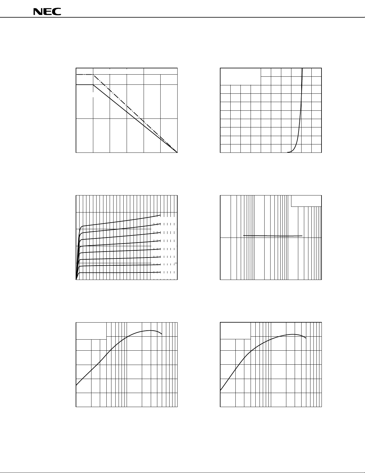
TOTAL POWER DISSIPATION vs.
AMBIENT TEMPERATURE
230
200
(mW)
T
2 Elements in total Free Air
Per
Element
100
Total Power Dissipation P
0
0 50 100 150
Ambient Temperature TA (°C)
COLLECTOR CURRENT vs.
COLLECTOR TO EMITTER VOLTAGE
25
20
(mA)
C
15
IB = 160 A
IB = 140 A
IB = 120 A
10
IB = 100 A
IB = 80 A
5
Collector Current I
IB = 60 A
IB = 40 A
0
0123456
IB = 20 A
Collector to Emitter Voltage VCE (V)
COLLECTOR CURRENT vs. BASE TO
EMITTER VOLTAGE
20
VCE = 3 V
(mA)
C
10
Collector Current I
0
0 0.5 1.0
Base to Emitter Voltage VBE (V)
DC CURRENT GAIN vs.
COLLECTOR CURRENT
1 000
VCE = 3 V
µ
FE
µ
µ
100
µ
µ
µ
DC Current Gain h
µ
µ
10
0.1 1 10 100
Collector Current IC (mA)
GAIN BANDWIDTH PRODUCT vs.
COLLECTOR CURRENT
6.00
VCE = 3 V
f = 1 GHz
5.00
(GHz)
T
4.00
3.00
2.00
1.00
Gain Bandwidth Product f
0.00
1 10 100
Collector Current IC (mA)
INSERTION POWER GAIN vs.
COLLECTOR CURRENT
14.00
VCE = 3 V
f = 1 GHz
12.00
(dB)
2
21e
10.00
8.00
6.00
4.00
Insertion Power Gain S
2.00
1 10 100
Collector Current IC (mA)
Data Sheet P14550EJ1V0DS00 3

µ
PA810TC
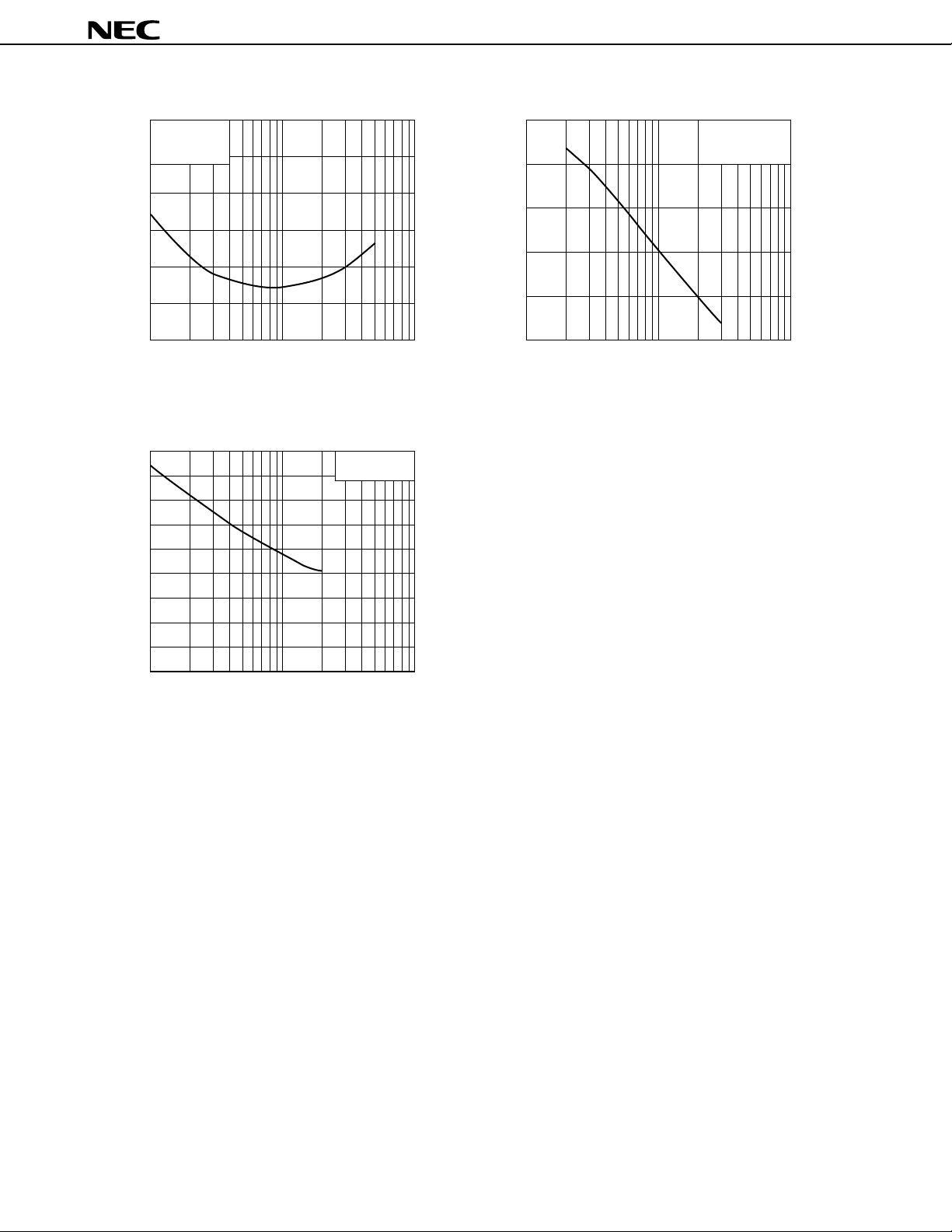
NOISE FIGURE vs. COLLECTOR CURRENT
6.00
VCE = 3 V
f = 1 GHz
5.00
4.00
3.00
2.00
Noise Figure NF (dB)
1.00
0.00
1 10 100
Collector Current IC (mA)
FEEDBACK CAPACITANCE vs.
COLLECTOR TO BASE VOLTAGE
0.900
0.800
(pF)
0.700
re
0.600
0.500
0.400
0.300
0.200
Feedback Capacitance C
0.100
0.000
1 10 100
Collector to Base Voltage VCB (V)
f = 1 MHz
INSERTION POWER GAIN vs. FREQUENCY
25.0
(dB)
2
20.0
21e
15.0
10.0
5.0
Insertion Power Gain S
0.0
0.1 1.0 10.0
Frequency f (GHz)
VCE = 3 V
I
C
= 7 mA
4 Data Sheet P14550EJ1V0DS00
 Loading...