

Motorola MC13055D, MC13055P Datasheet
The MC13055 is intended fo RF data link systems using carrier
frequencies up to 40 MHz and FSK (frequency shift keying) data rates up to
2.0 M Baud (1.0 MHz). This design is similar to the MC3356, except that it
does not include the oscillator/mixer. The IF bandwidth has been increased
and the detector output has been revised to a balanced configuration. The
received signal strength metering circuit has been retained, as has the
versatile data slicer/comparator.
• Input Sensitivity 20 µV @ 40 MHz
• Signal Strength Indicator Linear Over 3 Decades
• Available in Surface Mount Package
• Easy Application, Few Peripheral Components
Order this document by MC13055/D
WIDEBAND
FSK
RECEIVER
SEMICONDUCTOR
TECHNICAL DATA
P SUFFIX
PLASTIC PACKAGE
CASE 648
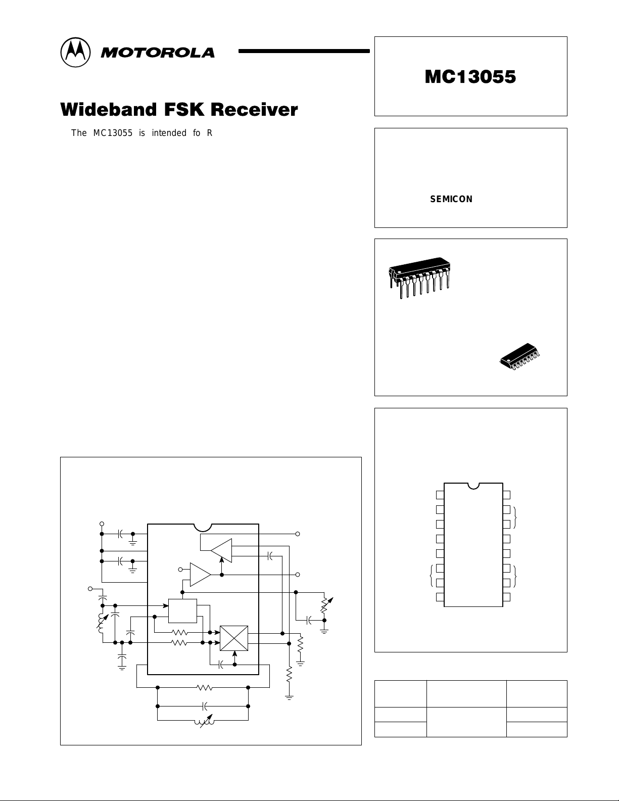
40MHz
IF
Input
Ω
)
(50
Figure 1. Block Diagram and Application Circuit
V
CC
L1
22pF
0.01
0.01
0.01
27pF
0.1
1
2
3
0.8V
4
5
6
7
V
8
CC
–
+
Limiter
1.0k
39pF
L2
16
15
+
14
–
100pF
13
12
11
10
9
Data
Output
Carrier
Detect
68pF
3.9k
5.0k
3.9k
Squelch
Adjust
(meter)
D SUFFIX
PLASTIC PACKAGE
CASE 751B
(SO–16)
PIN CONNECTIONS
Comparator Gnd
Comparator V
CC
IF Ground
IF V
CC
Limiter Input
Limiter Bias
Quad Bias
ORDERING INFORMATION
Device
MC13055D
MC13055P
Temperature Range
1
2
3
4
5
6
7
8
Operating
TA = – 40 to +85°C
16
Data Out
+
15
Comparator
–
14
13
Carrier Detect
12
Meter Drive
11
Detector
10
Out
9
Quad Input
Package
Plastic DIP
SO–16
MOTOROLA ANALOG IC DEVICE DATA
Motorola, Inc. 1996 Rev 2
1
MC13055
MAXIMUM RATINGS
Rating Symbol Value Unit
Power Supply Voltage V
Operating Supply Voltage Range V2, V4 3.0 to 12 Vdc
Junction Temperature T
Operating Ambient Temperature Range T
Storage Temperature Range T
Power Dissipation, Package Rating P
CC(max)
J
A
stg
D
15 Vdc
150 °C
–40 to +85 °C
–65 to +150 °C
1.25 W
ELECTRICAL CHARACTERISTICS (V
Characteristic Conditions Min Typ Max Unit
Total Drain Current 12 + 14 – 20 25 mA
Data Comparator Pull–Down Current I16 – 10 – mA
Meter Drive Slope versus Input I12 4.5 7.0 9.0 µA/dB
Carrier Detect Pull–Down Current I13 – 1.3 – mA
Carrier Detect Pull–Up Current I13 – 500 – µA
Carrier Detect Threshold Voltage V12 690 800 1010 mV
DC Output Current I10, I11 – 430 – µA
Recovered Signal V10 – V11 – 350 – mVrms
Sensitivity for 20 dB S + N/N, BW = 5.0 MHz VIN – 20 – µVrms
S + N/N at Vin = 50 µV V10 – V11 – 30 – dB
Input Impedance @ 40 MHz R
Quadrature Coil Loading R
= 5.0 Vdc, fo = 40 MHz, f
CC
Pin 5, Ground –
in
C
in
in
C
in
= 1.0 MHz, ∆f = ±1.0 MHz, TA = 25°C, test circuit of Figure 2.)
mod
Pin 9 to 8 –
–
–
4.2
4.5
7.6
5.2
–
–
–
–
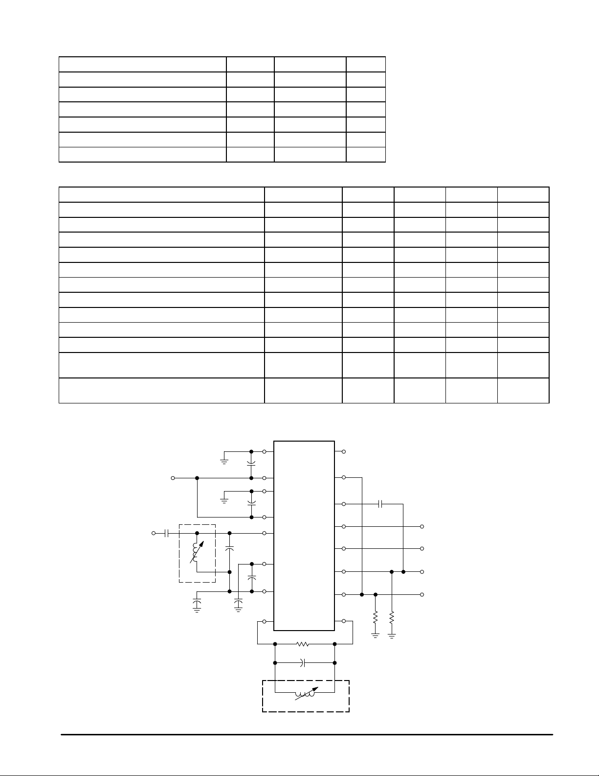
Figure 2. T est Circuit
1
16
kΩ
pF
kΩ
pF
Input
V
CC
22pF
L1
0.01
0.01
27pF
0.010.01
0.1
2
3
4
5
6
7
8
1.0k
39pF
L2
2
15
14
13
12
11
10
100pF
Carrier
Detect Output
Meter Drive
Detector
Output
9
3.9k3.9k
Coils – Shielded
Coilcraft UNI–10/142
L1 Gray 8–1/2 Turns, nominal 300 nH
L2 Black 10–1/2 Turns, nominal 380 nH
MOTOROLA ANALOG IC DEVICE DATA
MC13055
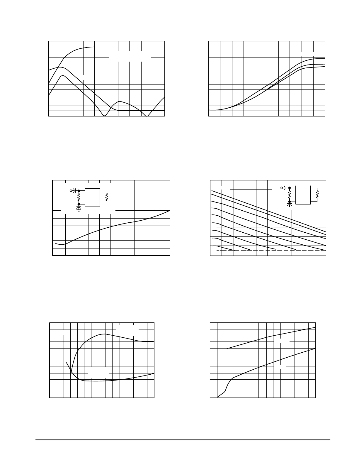
Figure 3. Overall Gain, Noise, AM Rejection Figure 4. Meter Current versus Signal
0
Output f
–10
mod
∆
f = 1.0 MHz
–20
–30
Noise
–40
–50
AMR 1.0 kHz
30%
RELATIVE OUTPUT (dB)
–60
–100
SIGNAL INPUT (dBm)
Figure 5. Untuned Input: Limiting Sensitivity
versus Frequency
–10
–20
–30
–40
–50
–60
–70
–80
, INPUT LIMITING SENSITIVITY (dBm)
–90
IN
V
–100
0
Input
10
0.1
0.1
5
51
7
MC13055
9
20k
8
f, INPUT FREQUENCY (MHz)
= 1.0 MHz
µ
600
500
400
VCC = 5.0 V, 7.0 V
3.0 V
12 V
300
200
l12, METER CURRENT ( A)
100
0–20–60 –40–80
0
–100
0–20–40–60–80
INPUT SIGNAL (dBm)
Figure 6. Untuned Input: Meter Current
versus Frequency
800
Input 0 dBm
700
–10
µ
600
–20
500
–30
–40
400
–50
300
–60
200
–70
l12, METER CURRENT ( Adc)
100
–80
0
10090807060504030200
f, INPUT FREQUENCY (MHz)
Input
0.1
0.1
MC13055
9
20k
8
5
51
7
1009080706050403020100
Figure 7. Limiting Sensitivity and Detuning
versus Supply V oltage
–40
–50
–60
–70
–80
, INPUT LIMITING SENSITIVITY (dBm)
–90
IN
V
40 MHz
Limiting
Sensitivity
VCC, SUPPLY VOLTAGE (Vdc)
Quadrature
Coil Tuning
119.05.0 7.03.00
MOTOROLA ANALOG IC DEVICE DATA
Figure 8. Detector Current and Power Supply
Current versus Supply Voltage
40 3
40.2
40.1
40.0
39.9
1200
µ
1000 50
I10 + I11
800
39.8
l10 + l11, DETECTOR CURRENT ( Adc)
600
400
200
I2 + I4
0
1.0
7.05.03.00
39.7
39.6
39.5
39.4
QUAD COIL TUNING (MHz)
39.3
39.2
15
131.0
VCC, SUPPLY VOLTAGE (Vdc)
60
40
30
20
10
l2 + I4, POWER SUPPLY CURRENT (mA)
0
13 15119.0
3
 Loading...