

SEMICONDUCTOR TECHNICAL DATA
The MC10/100E445 is an integrated 4-bit serial to parallel data
converter. The device is designed to operate for NRZ data rates of up to
2.0Gb/s. The chip generates a divide by 4 and a divide by 8 clock for both
4-bit conversion and a two chip 8-bit conversion function. The conversion
sequence was chosen to convert the first serial bit to Q0, the second to
Q1 etc.
• On-Chip Clock ÷4 and ÷8
• 2.0Gb/s Data Rate Capability
• Differential Clock and Serial Inputs
• V
Output for Single-Ended Input Applications
BB
PARALLEL CONVERTER
4-BIT SERIAL/
• Asynchronous Data Synchronization
• Mode Select to Expand to 8-Bits
• Internal 75kΩ Input Pulldown Resistors
• Extended 100E V
Two selectable serial inputs provide a loopback capability for testing
purposes when the device is used in conjunction with the E446 parallel to
serial converter.
The start bit for conversion can be moved using the SYNC input. A
single pulse applied asynchronously for at least two input clock cycles
shifts the start bit for conversion from Qn to Qn–1. For each additional
shift required an additional pulse must be applied to the SYNC input.
Asserting the SYNC input will force the internal clock dividers to “swallow”
a clock pulse, effectively shifting a bit from the Qn to the Qn–1 output (see
Timing Diagram B).
The MODE input is used to select the conversion mode of the device. With the MODE input LOW, or open, the device will
function as a 4-bit converter. When the mode input is driven HIGH the data on the output will change on every eighth clock cycle
thus allowing for an 8-bit conversion scheme using two E445’s. When cascaded in an 8-bit conversion scheme the devices will
not operate at the 2.0Gb/s data rate of a single device. Refer to the applications section of this data sheet for more information on
cascading the E445.
For lower data rate applications a VBB reference voltage is supplied for single-ended inputs. When operating at clock rates
above 500MHz differential input signals are recommended. For single-ended inputs the VBB pin is tied to the inverting differential
input and bypassed via a 0.01µF capacitor. The VBB provides the switching reference for the input differential amplifier . The V
can also be used to AC couple an input signal, for more information on AC coupling refer to the interfacing section of the design
guide in the ECLinPS data book.
Upon power-up the internal flip-flops will attain a random state. To synchronize multiple E445’s in a system the master reset
must be asserted.
Range of –4.2V to –5.46V
EE
FN SUFFIX
PLASTIC PACKAGE
CASE 776-02
BB
PIN NAMES
Pin Function
SINA, SINA
SINB, SINB
SEL
Q0–Q3
CLK, CLK
CL/4, CL/4
CL/8, CL/8
MODE
SYNCH
Differential Serial Data Input A
Differential Serial Data Input B
Serial Input Selector Pin
Parallel Data Outputs
Differential Clock Inputs
Differential ÷4 Clock Output
Differential ÷8 Clock Output
Conversion Mode 4-Bit/8-Bit
Conversion Synchronizing Input
FUNCTION TABLES
Mode Conversion SEL Serial Input
L
H
8/97
Motorola, Inc. 1997
4-Bit
8-Bit
H
L
1
V
CL/4
NCMODESINASINA
CCO
CCO
19202122232425
18
17
16
15
14
13
12
111098765
Q3V
SOUT
SOUT
V
CC
Q0
Q1
V
CCO
Q2
SYNC
RESET
SINB
26
SINB
27
SEL
28
V
EE
CLK
CLK
V
BB
A
B
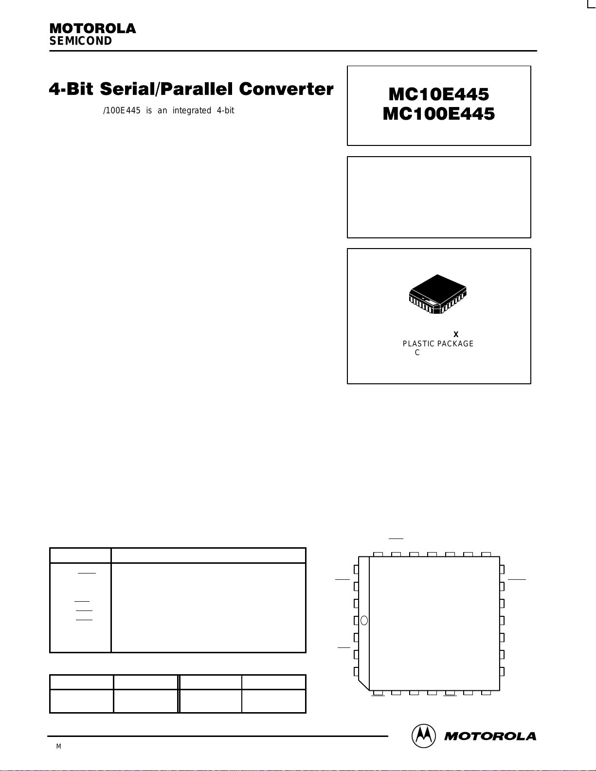
Figure 1. 28–Lead Pinout
1
2
3
4
REV 3
CL/8CL/8
(Top View)
CL/4V
CCO
MC10E445 MC100E445
SINB
SINB
SINA
SINA
SEL
QD
QD Q2QD
QD Q1QD
QD Q0QD
QD
Q3
MODE
CLK
CLK
SYNC
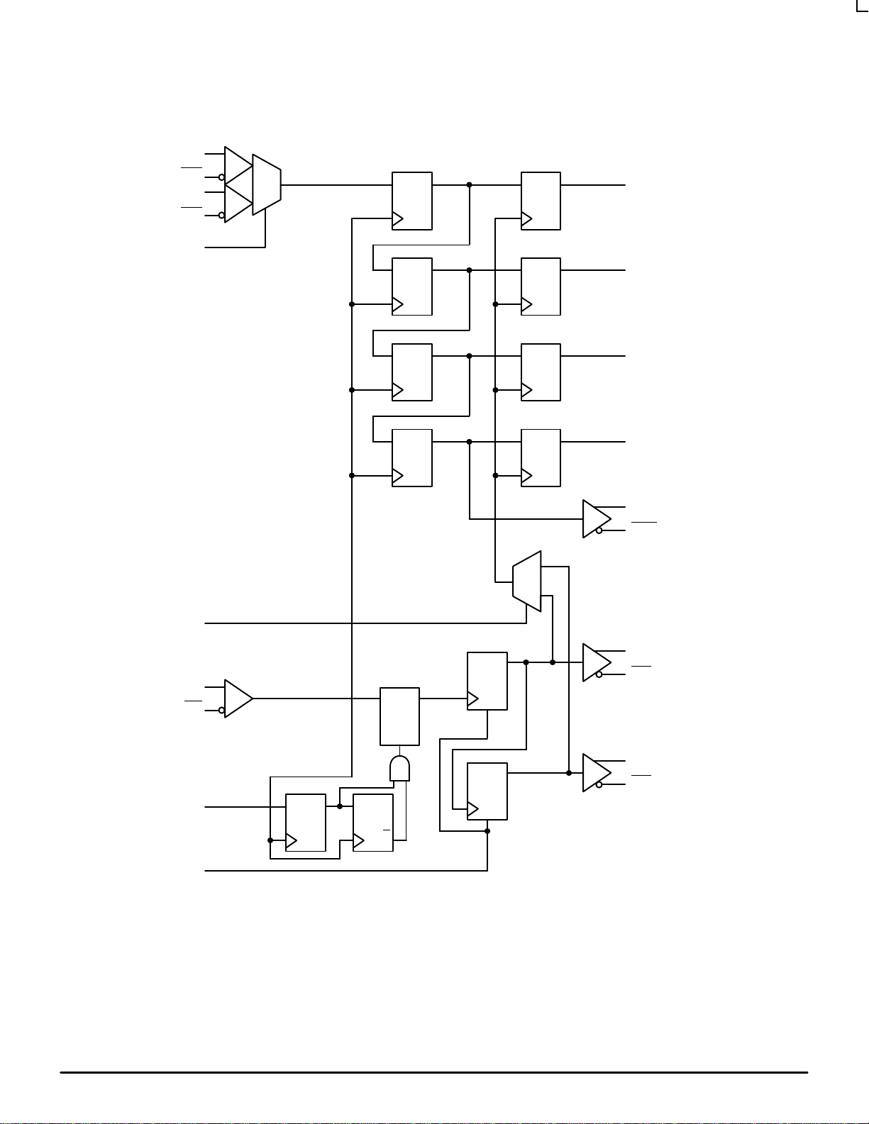
RESET
OutIn
Latch
EN
QD
D
Q
Figure 2. Logic Diagram
SOUT
SOUT
0
1
Out
÷
4
R
Out
÷
2
R
CL/4
CL/4
CL/8
CL/8
MOTOROLA ECLinPS and ECLinPS Lite
2
DL140 — Rev 4
MC10E445 MC100E445
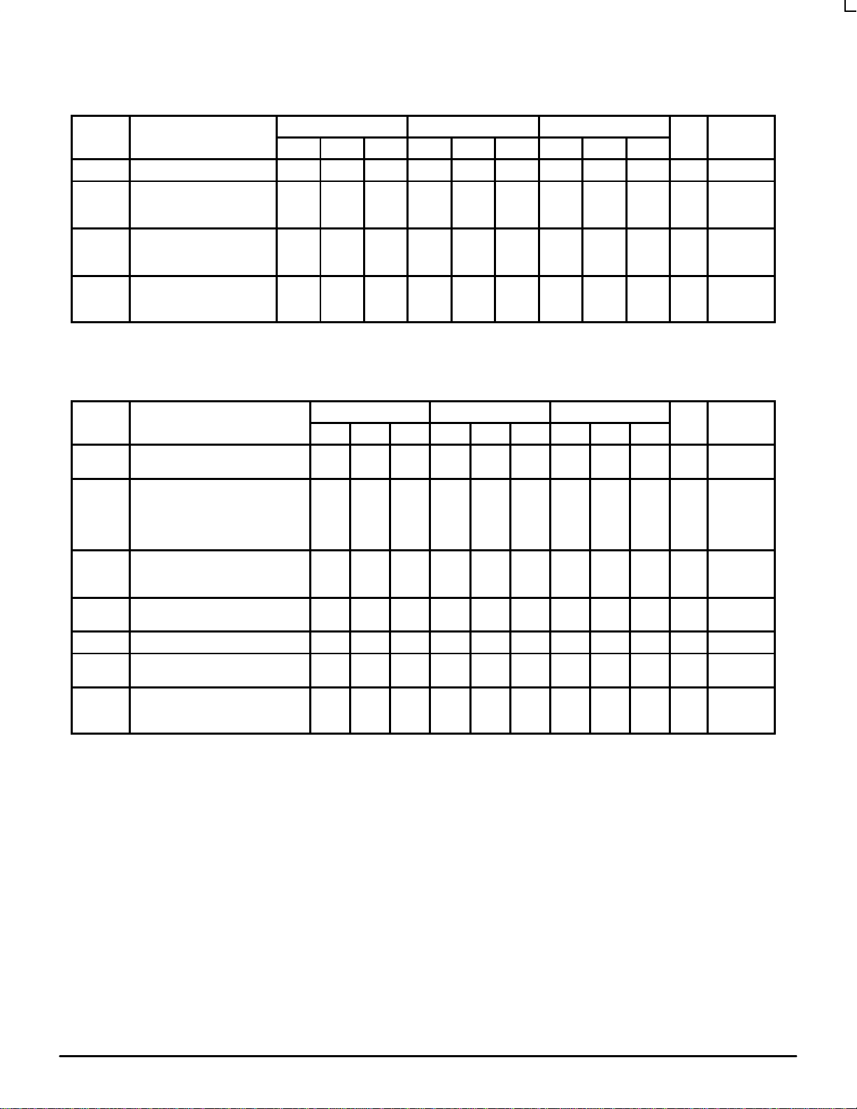
DC CHARACTERISTICS (VEE = VEE(min) to VEE(max); VCC = V
0°C 25°C 85°C
Symbol Characteristic Min Typ Max Min Typ Max Min Typ Max Unit Condition
I
IH
V
OH
V
BB
I
EE
1. The maximum VOH limit was relaxed from standard ECL due to the high frequency output design. All other outputs are specified with the standard
10E and 100E VOH levels.
Input HIGH Current 150 150 150 µA
Ouput HIGH Current
10E (SOUT Only)
100E (SOUT Only)
Output Reference Voltage
10E
100E
Power Supply Current
10E
100E
–1020
–1025
–1.38
–1.38
154
154
–790
–830
–1.27
–1.26
185
185
–980
–1025
–1.35
–1.38
AC CHARACTERISTICS (VEE = VEE(min) to VEE(max); VCC = V
0°C 25°C 85°C
Symbol Characteristic Min Typ Max Min Typ Max Min Typ Max Unit Condition
f
MAX
t
PLH
t
PHL
t
s
t
h
t
RR
t
PW
t
r
t
f
Maximum Conversion Frequency 2.0 2.0 2.0 Gb/s
Propagation Delay to Output
CLK to Q
CLK to SOUT
CLK to CL/4
CLK to CL/8
Setup Time
SINA, SINB
SEL
Hold Time
SINA, SINB, SEL
Reset Recovery Time 500 300 500 300 500 300 ps
Minimum Pulse Width
CLK, MR
Rise/Fall Times
SOUT
Other
1500
1800
975
1325
1325
–200
225
425
2100
1150
1550
1550
350
650
800
1100
1100
–1000–250
450 300 450 300 450 300
400 400 400
100
200
= GND)
CCO
154
154
= GND)
CCO
1500
1800
800
100
200
975
1325
1325
–200
225
425
1100
1100
–1000–250
–760
–830
–1.25
–1.26
185
185
2100
1150
1550
1550
350
650
–910
–1025
–1.31
–1.38
1500
800
1100
1100
–1000–250
100
200
154
177
1800
975
1325
1325
–200
225
425
–670
–830
–1.19
–1.26
185
212
2100
1150
1550
1550
350
650
V
1
1
V
mA
NRZ
ps
ps
ps
ps
ps 20%–80%
DL140 — Rev 4
3 MOTOROLAECLinPS and ECLinPS Lite

MC10E445 MC100E445
CLK
Figure 3. Timing Diagrams
SIN
RESET
Q0
Q1
Q2
Q3
SOUT
CL/4
CL/8
CLK
SIN
RESET
Dn-4 Dn-3 Dn-2 Dn-1 Dn Dn+1 Dn+2 Dn+3
Dn-4
Dn-3
Dn-2
Dn-1
Dn-4 Dn-3 Dn-2 Dn-1 Dn Dn+1 Dn+2 Dn+3
Timing Diagram A. 1:4 Serial to Parallel Conversion
Dn-4 Dn-3 Dn-2 Dn-1 Dn Dn+1 Dn+2 Dn+3
Dn
Dn+1
Dn+2
Dn+3
Dn+4
SYNC
Q0
Q1
Q2
Q3
SOUT
CL/4
CL/8
Dn-4
Dn-3
Dn-2
Dn-1
Dn-4 Dn-3 Dn-2 Dn-1 Dn Dn+1 Dn+2 Dn+3
Dn+1
Dn+2
Dn+3
Dn+4
Timing Diagram B. 1:4 Serial to Parallel Conversion With SYNC Pulse
Dn+4
MOTOROLA ECLinPS and ECLinPS Lite
4
DL140 — Rev 4

APPLICATIONS INFORMATION
MC10E445 MC100E445
The MC10E/100E445 is an integrated 1:4 serial to parallel
converter. The chip is designed to work with the E446 device
to provide both transmission and receiving of a high speed
serial data path. The E445, can convert up to a 2.0Gb/s NRZ
data stream into 4-bit parallel data. The device also provides
a divide by four clock output to be used to synchronize the
parallel data with the rest of the system.
The E445 features multiplexed dual serial inputs to
provide test loop capability when used in conjunction with the
E446. Figure 4 illustrates the loop test architecture. The
architecture allows for the electrical testing of the link without
requiring actual transmission over the serial data path
medium. The SINA serial input of the E445 has an extra
buffer delay and thus should be used as the loop back serial
input.
PARALLEL
DATA
PARALLEL
DATA
SOUT
SOUT
SINA
SINA
SINB
SINB
TO SERIAL
MEDIUM
FROM
SERIAL
MEDIUM
increased. The delay between the two clocks can be
increased until the minimum delay of clock to serial out would
potentially cause a serial bit to be swallowed (Figure 6).
CLOCK
CLOCK
CLOCK
Tpd CLK
to SOUT
SERIAL
INPUT
DATA
E445a
SOUT
SIN
SOUT
SIN
Q3Q7Q2Q6Q1Q5Q0
Q4
PARALLEL OUTPUT DAT A
800ps
1150ps
E445b
SIN
SIN
Q3Q3Q2Q2Q1Q1Q0
Q0
100ps
Figure 4. Loopback T est Architecture
The E445 features a differential serial output and a divide
by 8 clock output to facilitate the cascading of two devices to
build a 1:8 demultiplexer . Figure 5 illustrates the architecture
for a 1:8 demultiplexer using two E445’s; the timing diagram
for this configuration can be found on the following page.
Notice the serial outputs (SOUT) of the lower order converter
feed the serial inputs of the the higher order device. This feed
through of the serial inputs bounds the upper end of the
frequency of operation. The clock to serial output
propagation delay plus the setup time of the serial input pins
must fit into a single clock period for the cascade architecture
to function properly. Using the worst case values for these
two parameters from the data sheet, TPD CLK to SOUT =
1 150ps and tS for SIN = –100ps, yields a minimum period of
1050ps or a clock frequency of 950MHz.
The clock frequency is significantly lower than that of a
single converter, to increase this frequency some games can
be played with the clock input of the higher order E445. By
delaying the clock feeding the second E445 relative to the
clock of the first E445 the frequency of operation can be
Figure 5. Cascaded 1:8 Converter Architecture
With a minimum delay of 800ps on this output the clock for
the lower order E445 cannot be delayed more than 800ps
relative to the clock of the first E445 without potentially
missing a bit of information. Because the setup time on the
serial input pin is negative coincident excursions on the data
and clock inputs of the E445 will result in correct operation.
CLOCK A
CLOCK B
Tpd CLK
to SOUT
800ps
1150ps
Figure 6. Cascade Frequency Limitation
DL140 — Rev 4
5 MOTOROLAECLinPS and ECLinPS Lite

MC10E445 MC100E445
Perhaps the easiest way to delay the second clock relative
to the first is to take advantage of the differential clock inputs
of the E445. By connecting the clock for the second E445 to
the complimentary clock input pin the device will clock a half
a clock period after the first E445 (Figure 7). Utilizing this
simple technique will raise the potential conversion
CLOCK
CLOCK
SERIAL
INPUT
DATA
E445a
SIN
SOUT
SIN
SOUT
Q3Q7Q2Q6Q1Q5Q0
Q4
PARALLEL OUTPUT DATA
E445b
SIN
SIN
Q3Q3Q2Q2Q1Q1Q0
Q0
Figure 7. Extended Frequency 1:8 Demultiplexer
CLK
frequency up to 1.4GHz. The divide by eight clock of the
second E445 should be used to synchronize the parallel data
to the rest of the system as the parallel data of the two E445’s
will no longer be synchronized. This skew problem between
the outputs can be worked around as the parallel information
will be static for eight more clock pulses.
CLOCK A
CLOCK B
Tpd CLK
to SOUT
700ps
(1.4GHz)
800ps
1150ps
100ps
SINa
Q0
Q1
Q2
Q3
Q4 (Q0 a)
Q5 (Q1 a)
Q6 (Q2 a)
Q7 (Q3 a)
SOUTa
SOUTb
CL/4a
CL/4b
CL/8a
CL/8b
Dn-4 Dn-3 Dn-2 Dn-1 Dn Dn+1 Dn+2 Dn+3
Dn-4
Dn-3
Dn-2
Dn-1
Dn
Dn+1
Dn+2
Dn+3
Dn-4 Dn-3 Dn-2 Dn-1 Dn Dn+1 Dn+2 Dn+3
Dn-4 Dn-3 Dn-2 Dn-1 Dn Dn+1
Figure 8. Timing Diagram A. 1:8 Serial to Parallel Conversion
MOTOROLA ECLinPS and ECLinPS Lite
6
DL140 — Rev 4

-L-
28 1
-N-
MC10E445 MC100E445
OUTLINE DIMENSIONS
FN SUFFIX
PLASTIC PLCC PACKAGE
CASE 776–02
ISSUE D
SNSM
0.007 (0.180) T L
Y BRK
B
0.007 (0.180) T L
U
D
Z
-M-
D
W
V
X
VIEW D-D
–M
G1
0.010 (0.250) T L
–M
SNSM
SNSS
–M
Z
C
G
G1
0.010 (0.250) T L
0.007 (0.180) T L
A
0.007 (0.180) T L
R
E
0.004 (0.100)
J
PLANE
SEATING
-T-
VIEW S
SNSS
–M
NOTES:
1. DATUMS -L-, -M-, AND -N- DETERMINED
WHERE TOP OF LEAD SHOULDER EXITS
PLASTIC BODY AT MOLD PARTING LINE.
2. DIM G1, TRUE POSITION TO BE MEASURED
AT DATUM -T-, SEATING PLANE.
3. DIM R AND U DO NOT INCLUDE MOLD FLASH.
ALLOWABLE MOLD FLASH IS 0.010 (0.250)
PER SIDE.
4. DIMENSIONING AND TOLERANCING PER ANSI
Y14.5M, 1982.
5. CONTROLLING DIMENSION: INCH.
6. THE PACKAGE TOP MAY BE SMALLER THAN
THE PACKAGE BOTTOM BY UP TO 0.012
(0.300). DIMENSIONS R AND U ARE
DETERMINED AT THE OUTERMOST
EXTREMES OF THE PLASTIC BODY
EXCLUSIVE OF MOLD FLASH, TIE BAR
BURRS, GATE BURRS AND INTERLEAD
FLASH, BUT INCLUDING ANY MISMATCH
BETWEEN THE TOP AND BOTTOM OF THE
PLASTIC BODY.
7. DIMENSION H DOES NOT INCLUDE DAMBAR
PROTRUSION OR INTRUSION. THE DAMBAR
PROTRUSION(S) SHALL NOT CAUSE THE H
DIMENSION TO BE GREATER THAN 0.037
(0.940). THE DAMBAR INTRUSION(S) SHALL
NOT CAUSE THE H DIMENSION TO BE
SMALLER THAN 0.025 (0.635).
–M
–M
SNSM
SNSM
H
0.007 (0.180) T L
–M
SNSM
K1
K
SNSM
0.007 (0.180) T L
F
–M
VIEW S
INCHES MILLIMETERS
MIN MINMAX MAX
DIM
G1
K1
A
B
C
E
F
G
H
J
K
R
U
V
W
X
Y
Z
0.485
0.485
0.165
0.090
0.013
0.050 BSC
0.026
0.020
0.025
0.450
0.450
0.042
0.042
0.042
—
°
2
0.410
0.040
0.495
0.495
0.180
0.110
0.019
0.032
—
—
0.456
0.456
0.048
0.048
0.056
0.020
10
0.430
—
12.32
12.57
12.32
12.57
4.20
4.57
2.29
2.79
0.33
0.48
1.27 BSC
0.66
0.81
0.51
—
0.64
—
11.43
11.58
11.43
11.58
1.07
1.21
1.07
1.21
1.07
1.42
—
0.50
°
°
2
1.02
10
10.92
—
°
10.42
DL140 — Rev 4
7 MOTOROLAECLinPS and ECLinPS Lite

MC10E445 MC100E445
Motorola reserves the right to make changes without further notice to any products herein. Motorola makes no warranty , representation or guarantee regarding
the suitability of its products for any particular purpose, nor does Motorola assume any liability arising out of the application or use of any product or circuit, and
specifically disclaims any and all liability, including without limitation consequential or incidental damages. “T ypical” parameters which may be provided in Motorola
data sheets and/or specifications can and do vary in different applications and actual performance may vary over time. All operating parameters, including “Typicals”
must be validated for each customer application by customer’s technical experts. Motorola does not convey any license under its patent rights nor the rights of
others. Motorola products are not designed, intended, or authorized for use as components in systems intended for surgical implant into the body, or other
applications intended to support or sustain life, or for any other application in which the failure of the Motorola product could create a situation where personal injury
or death may occur. Should Buyer purchase or use Motorola products for any such unintended or unauthorized application, Buyer shall indemnify and hold Motorola
and its officers, employees, subsidiaries, affiliates, and distributors harmless against all claims, costs, damages, and expenses, and reasonable attorney fees
arising out of, directly or indirectly, any claim of personal injury or death associated with such unintended or unauthorized use, even if such claim alleges that
Motorola was negligent regarding the design or manufacture of the part. Motorola and are registered trademarks of Motorola, Inc. Motorola, Inc. is an Equal
Opportunity/Affirmative Action Employer.
How to reach us:
USA/EUROPE/ Locations Not Listed: Motorola Literature Distribution; JAPAN: Nippon Motorola Ltd.: SPD, Strategic Planning Office, 4–32–1,
P.O. Box 5405, Denver, Colorado 80217. 1–303–675–2140 or 1–800–441–2447 Nishi–Gotanda, Shinagawa–ku, Tokyo 141, Japan. 81–3–5487–8488
Customer Focus Center: 1–800–521–6274
Mfax: RMFAX0@email.sps.mot.com – TOUCHTONE 1–602–244–6609 ASIA/PACIFIC: Motorola Semiconductors H.K. Ltd.; 8B Tai Ping Industrial Park,
Moto rola Fax Bac k System – US & Canada ONLY 1–800–774–1848 51 Ting Kok Road, Tai Po, N.T., Hong Kong. 852–26629298
HOME PAGE: http://motorola.com/sps/
– http://sps.motorola.com/mfax/
◊
MOTOROLA ECLinPS and ECLinPS Lite
8
Mfax is a trademark of Motorola, Inc.
MC10E445/D
DL140 — Rev 4

WWW.ALLDATASHEET.COM
Copyright © Each Manufacturing Company.
All Datasheets cannot be modified without permission.
This datasheet has been download from :
www.AllDataSheet.com
100% Free DataSheet Search Site.
Free Download.
No Register.
Fast Search System.
www.AllDataSheet.com
 Loading...