

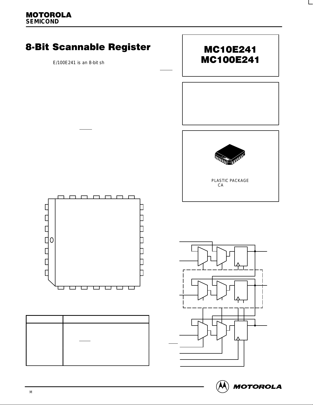
LOGIC DIAGRAM
SEL1
CLK
MR
V
EE
S-IN
D
0
D
1
26
27
28
2
3
4
25 24 23 22 21 20 19
18
17
16
15
14
13
12
115 6 7 8 9 10
SEL0 NC D7D6D5V
CCOQ7
Q
6
Q
5
V
CC
NC
V
CCO
Q
4
Q
3
D2D3D4V
CCOQ0Q1Q2
Q
0
Q1 – Q
6
Q
7
S-IN
D
0
D1 – D
6
D
7
HOLD/LOAD
SHIFT
CLK
MR
BITS 1–6
D
D
D
Q
Q
Q
R
R
R
1
Pinout: 28-Lead PLCC (Top View)
* All VCC and V
CCO
pins are tied together on the die.
SEMICONDUCTOR TECHNICAL DATA
2–1
REV 3
Motorola, Inc. 1996
7/96
The MC10E/100E241 is an 8-bit shiftable register. Unlike a standard
universal shift register such as the E141, the E241 features internal data
feedback organized so that the SHIFT control overrides the HOLD/LOAD
control. This enables the normal operations of HOLD and LOAD to be
toggled with a single control line without the need for external gating. It
also enables switching to scan mode with the single SHIFT control line.
The eight inputs D0– D7 accept parallel input data, while S-IN accepts
serial input data when in shift mode. Data is accepted a set-up time
before the positive-going edge of CLK; shifting is also accomplished on
the positive clock edge. A HIGH on the Master Reset pin (MR)
asynchronously resets all the registers to zero.
• SHIFT overrides HOLD/LOAD Control
• 1000ps Max. CLK to Q
• Asynchronous Master Reset
• Pin-Compatible with E141
• Extended 100E V
EE
Range of – 4.2V to – 5.46V
• 75kΩ Input Pulldown Resistors
PIN NAMES
Pin Function
D0– D
7
Parallel Date Inputs
S-IN Serial Data Inputs
SEL0 SHIFT Control
SEL1 HOLD/LOAD Control
CLK Clock
MR Master Reset
Q0– Q
7
Data Outputs
8-BIT SCANNABLE
REGISTER
FN SUFFIX
PLASTIC PACKAGE
CASE 776-02
MC10E241 MC100E241
MOTOROLA ECLinPS and ECLinPS Lite
DL140 — Rev 4
2–2
DC CHARACTERISTICS (VEE = VEE(min) to VEE(max); VCC = V
CCO
= GND)
0°C 25°C 85°C
Symbol Characteristic min typ max min typ max min typ max Unit Condition
I
IH
Input HIGH Current 150 150 150 µA
I
EE
Power Supply Current MA
10E 125 150 125 150 125 150
100E 125 150 125 150 144 173
AC CHARACTERISTICS (VEE = VEE(min) to VEE(max); VCC = V
CCO
= GND)
0°C 25°C 85°C
Symbol Characteristic min typ max min typ max min typ max Unit Condition
f
SHIFT
Max. Shift Frequency 700 900 700 900 700 900 MHz
t
PLH
Propagation Delay to Output ps
t
PHL
Clk 625 750 975 625 750 975 625 750 975
MR 600 725 975 600 725 975 600 725 975
t
s
Setup Time ps
D 175 25 175 25 175 25
SEL0 (SHIFT) 350 200 350 200 350 200
SEL1 (HOLD/LOAD) 400 250 400 250 400 250
S-IN 125 –100 125 –100 125 –100
t
h
Hold Time ps
D 200 – 25 200 – 25 200 – 25
SEL0 (SHIFT) 100 – 200 100 – 200 100 – 200
SEL1 (HOLD/LOAD) 50 – 250 50 – 250 50 – 250
S-IN 300 100 300 100 300 100
t
RR
Reset Recovery Time 900 600 900 600 900 600 ps
t
PW
Minimum Pulse Width ps
Clk, MR 400 400 400
t
SKEW
Within-Device Skew 60 60 60 ps 1
t
r
Rise/Fall Times ps
t
f
20 - 80% 300 525 800 300 525 800 300 525 800
1. Within-device skew is defined as identical transitions on similar paths through a device.
FUNCTION TABLE
MR SEL0 SEL1 Function
1 X X Outputs LOW
0 1 X Shift Data
0 0 1 Hold Data
0 0 0 Load Data

MC10E241 MC100E241
2–3 MOTOROLAECLinPS and ECLinPS Lite
DL140 — Rev 4
OUTLINE DIMENSIONS
FN SUFFIX
PLASTIC PLCC PACKAGE
CASE 776–02
ISSUE D
0.007 (0.180) T L
–M
SNSM
0.007 (0.180) T L
–M
SNSM
0.007 (0.180) T L
–M
SNSM
0.010 (0.250) T L
–M
SNSS
0.007 (0.180) T L
–M
SNSM
0.010 (0.250) T L
–M
SNSS
0.007 (0.180) T L
–M
SNSM
0.007 (0.180) T L
–M
SNSM
0.004 (0.100)
SEATING
PLANE
-T-
12.32
12.32
4.20
2.29
0.33
0.66
0.51
0.64
11.43
11.43
1.07
1.07
1.07
—
2
°
10.42
1.02
12.57
12.57
4.57
2.79
0.48
0.81
—
—
11.58
11.58
1.21
1.21
1.42
0.50
10
°
10.92
—
1.27 BSC
A
B
C
E
F
G
H
J
K
R
U
V
W
X
Y
Z
G1
K1
MIN MINMAX MAX
INCHES MILLIMETERS
DIM
NOTES:
1. DATUMS -L-, -M-, AND -N- DETERMINED
WHERE TOP OF LEAD SHOULDER EXITS
PLASTIC BODY AT MOLD PARTING LINE.
2. DIM G1, TRUE POSITION TO BE MEASURED
AT DATUM -T-, SEATING PLANE.
3. DIM R AND U DO NOT INCLUDE MOLD FLASH.
ALLOWABLE MOLD FLASH IS 0.010 (0.250)
PER SIDE.
4. DIMENSIONING AND TOLERANCING PER ANSI
Y14.5M, 1982.
5. CONTROLLING DIMENSION: INCH.
6. THE PACKAGE TOP MAY BE SMALLER THAN
THE PACKAGE BOTTOM BY UP TO 0.012
(0.300). DIMENSIONS R AND U ARE
DETERMINED AT THE OUTERMOST
EXTREMES OF THE PLASTIC BODY
EXCLUSIVE OF MOLD FLASH, TIE BAR
BURRS, GATE BURRS AND INTERLEAD
FLASH, BUT INCLUDING ANY MISMATCH
BETWEEN THE TOP AND BOTTOM OF THE
PLASTIC BODY.
7. DIMENSION H DOES NOT INCLUDE DAMBAR
PROTRUSION OR INTRUSION. THE DAMBAR
PROTRUSION(S) SHALL NOT CAUSE THE H
DIMENSION TO BE GREATER THAN 0.037
(0.940). THE DAMBAR INTRUSION(S) SHALL
NOT CAUSE THE H DIMENSION TO BE
SMALLER THAN 0.025 (0.635).
VIEW S
B
U
Z
G1
X
VIEW D-D
H
K
F
VIEW S
G
C
Z
A
R
E
J
0.485
0.485
0.165
0.090
0.013
0.026
0.020
0.025
0.450
0.450
0.042
0.042
0.042
—
2
°
0.410
0.040
0.495
0.495
0.180
0.110
0.019
0.032
—
—
0.456
0.456
0.048
0.048
0.056
0.020
10
°
0.430
—
0.050 BSC
-N-
Y BRK
D
D
W
-M-
-L-
28 1
V
G1
K1

MC10E241 MC100E241
MOTOROLA ECLinPS and ECLinPS Lite
DL140 — Rev 4
2–4
Motorola reserves the right to make changes without further notice to any products herein. Motorola makes no warranty , representation or guarantee regarding
the suitability of its products for any particular purpose, nor does Motorola assume any liability arising out of the application or use of any product or circuit, and
specifically disclaims any and all liability , including without limitation consequential or incidental damages. “Typical” parameters which may be provided in Motorola
data sheets and/or specifications can and do vary in different applications and actual performance may vary over time. All operating parameters, including “Typicals”
must be validated for each customer application by customer’s technical experts. Motorola does not convey any license under its patent rights nor the rights of
others. Motorola products are not designed, intended, or authorized for use as components in systems intended for surgical implant into the body, or other
applications intended to support or sustain life, or for any other application in which the failure of the Motorola product could create a situation where personal injury
or death may occur. Should Buyer purchase or use Motorola products for any such unintended or unauthorized application, Buyer shall indemnify and hold Motorola
and its officers, employees, subsidiaries, affiliates, and distributors harmless against all claims, costs, damages, and expenses, and reasonable attorney fees
arising out of, directly or indirectly, any claim of personal injury or death associated with such unintended or unauthorized use, even if such claim alleges that
Motorola was negligent regarding the design or manufacture of the part. Motorola and are registered trademarks of Motorola, Inc. Motorola, Inc. is an Equal
Opportunity/Affirmative Action Employer.
How to reach us:
USA/EUROPE/Locations Not Listed: Motorola Literature Distribution; JAPAN: Nippon Motorola Ltd.; Tatsumi–SPD–JLDC, 6F Seibu–Butsuryu–Center,
P.O. Box 20912; Phoenix, Arizona 85036. 1–800–441–2447 or 602–303–5454 3–14–2 Tatsumi Koto–Ku, Tokyo 135, Japan. 03–81–3521–8315
MFAX: RMFAX0@email.sps.mot.com – TOUCHTONE 602–244–6609 ASIA/PACIFIC: Motorola Semiconductors H.K. Ltd.; 8B Tai Ping Industrial Park,
INTERNET: http://Design–NET.com 51 Ting Kok Road, Tai Po, N.T., Hong Kong. 852–26629298
MC10E241/D
*MC10E241/D*
◊

WWW.ALLDATASHEET.COM
Copyright © Each Manufacturing Company.
All Datasheets cannot be modified without permission.
This datasheet has been download from :
www.AllDataSheet.com
100% Free DataSheet Search Site.
Free Download.
No Register.
Fast Search System.
www.AllDataSheet.com
 Loading...