


To all our customers
Regarding the change of names mentioned in the document, such as Mitsubishi Electric and Mitsubishi XX, to Renesas Technology Corp.
The semiconductor operations of Hitachi and Mitsubishi Electric were transferred to Renesas Technology Corporation on April 1st 2003. These operations include microcomputer, logic, analog and discrete devices, and memory chips other than DRAMs (flash memory, SRAMs etc.) Accordingly, although Mitsubishi Electric, Mitsubishi Electric Corporation, Mitsubishi Semiconductors, and other Mitsubishi brand names are mentioned in the document, these names have in fact all been changed to Renesas Technology Corp. Thank you for your understanding. Except for our corporate trademark, logo and corporate statement, no changes whatsoever have been made to the contents of the document, and these changes do not constitute any alteration to the contents of the document itself.
Note : Mitsubishi Electric will continue the business operations of high frequency & optical devices and power devices.
Renesas Technology Corp.
Customer Support Dept.
April 1, 2003

MITSUBISHI MICROCOMPUTERS
M37212M4/M8–XXXSP, M37212M6–XXXSP/FP M37212EFSP/FP
SINGLE-CHIP 8-BIT CMOS MICROCOMPUTER for VOLTAGE SYNTHESIZER with ON-SCREEN DISPLAY CONTROLLER
1. DESCRIPTION
The M37212M6-XXXSP/FP, M37212M4/M8-XXXSP are single-chip microcomputers designed with CMOS silicon gate technology. They have a OSD, I2C-BUS interface, and PWM, so it is useful for a channel selection system for TV.
The feature of the M37212EFSP/FP are similar to those of the M37212M6-XXXSP/FP except that these chips have a built-in PROM which can be written electrically. The differences between the
M37212M6-XXXSP/FP and M37212M4/M8-XXXSP are the ROM size and the RAM size as shown below. Accordingly, the following descriptions will be for M37212M6-XXXSP/FP unless otherwise noted.
OSD function |
|
Display characters ................................... |
24 characters 2 lines |
(It is possible to display 3lines or more by software) |
|
Kinds of characters ........................................................ |
256 kinds |
Character display area .............................................. |
12 16 dots |
Kinds of character sizes ..................................................... |
3 kinds |
Kinds of character colors .................................. |
8 colors (R, G, B) |
Coloring unit ................... |
character, character background, raster |
Display position ............................................................................. |
|
Horizontal: 64 levels |
Vertical: 128 levels |
Attribute .............................................................................. |
border |
2. FEATURES |
|
|
●Number of basic instructions ..................................................... |
|
71 |
●Memory size |
|
|
ROM............... ......... |
16K bytes (M37212M4-XXXSP) |
|
|
24K bytes (M37212M6-XXXSP/FP) |
|
|
32K bytes (M37212M8-XXXSP) |
|
|
62K bytes (M37212EFSP/FP) |
|
RAM ......................... |
320 bytes (M37212M4-XXXSP) |
|
|
384 bytes (M37212M6-XXXSP/FP) |
|
|
576 bytes (M37212M8-XXXSP) |
|
|
1280 bytes (M37212EFSP/FP) |
|
(*ROM correction memory included) |
||
●The minimum instruction execution time |
|
|
......................................... 0.5 μs (at 8 MHz oscillation frequency) |
||
●Power source voltage .................................................. |
|
5 V ± 10 % |
●Subroutine nesting |
|
|
maximum 96 levels (M37212M4/M8-XXXSP, M37212M6-XXXSP/FP) |
||
maximum 128 levels (M37212EFSP/FP) |
|
|
●Interrupts ........................................................ |
|
14 types, 14 vectors |
●8-bit timers ................................................................................... |
|
4 |
●Programmable I/O ports |
|
|
(Ports P0, P10–P14, P2, P30, P31, P40, P41) |
............................. 25 |
|
●Input ports (Ports P15–P17, P32–P37, P42) ............................... |
10 |
|
●Output ports (Ports P52–P55, P60–P63) ....................................... |
8 |
|
●12 V withstand ports .................................................................. |
|
12 |
●LED drive ports ............................................................................ |
|
4 |
●Serial I/O ............................................................. |
|
8 - bit 1 channel |
●Multi-master I2C-BUS interface |
............................... |
1 (2 systems) |
●A-D comparator (6-bit resolution) ................................. |
8 channels |
|
●PWM output circuit .......................................... |
|
14 - bit 1, 8 - bit 8 |
●Power dissipation .............................................................. |
|
165 mW |
(at 8 MHz oscillation frequency, VCC=5.5V, at OSD display) |
||
●ROM correction function ................................................. |
|
2 vectors |
Note: Only M37212M8-XXXSP and M37212EFSP/FP have ROM |
||
correction function. |
|
|
3. APPLICATION
TV
Rev. 1.0

MITSUBISHI MICROCOMPUTERS
M37212M4/M8–XXXSP, M37212M6–XXXSP/FP
M37212EFSP/FP
SINGLE-CHIP 8-BIT CMOS MICROCOMPUTER for VOLTAGE SYNTHESIZER with ON-SCREEN DISPLAY CONTROLLER
TABLE OF CONTENTS |
|
1. DESCRIPTION .......................................................................... |
1 |
2. FEAUTURES ............................................................................. |
1 |
3. APPLICATION ............................................................................ |
1 |
4. PIN CONFIGURATION .............................................................. |
3 |
5. FUNCTIONAL BLOCK DIAGRAM ............................................. |
5 |
6. PERFORMANCE OVERVIEW ................................................... |
6 |
7. PIN DESCRIPTION ................................................................... |
8 |
8. FUNCTIONAL DESCRIPTION ................................................. |
12 |
8.1 CENTRAL PROCESSING UNIT (CPU) .................... |
12 |
8.2 MEMORY .................................................................. |
13 |
8.3 INTERRUPTS ........................................................... |
19 |
8.4 TIMERS ..................................................................... |
24 |
8.5 SERIAL I/O ................................................................ |
27 |
8.6 MULTI-MASTER I2C-BUS INTERFACE .................... |
31 |
8.7 PWM OUTPUT CIRCUIT .......................................... |
44 |
8.8 A-D COMPARATOR .................................................. |
49 |
8.9 ROM CORRECTION FUNCTION ............................. |
51 |
8.10 OSD FUNCTIONS ................................................... |
52 |
8.10.1 Display Position ....................................... |
56 |
8.10.2 Character Size ......................................... |
60 |
8.10.3 Clock for OSD .......................................... |
62 |
8.10.4 Memory for OSD ...................................... |
63 |
8.10.5 Color Register .......................................... |
66 |
8.10.6 Border ...................................................... |
68 |
8.10.7 Multiline Display ....................................... |
69 |
8.10.8 OSD Output Pin Control .......................... |
70 |
8.10.9 Raster Coloring Function ......................... |
71 |
8.11. SOFTWARE RUNAWAY DETECT FUNCTION ...... |
72 |
8.12. RESET CIRCUIT .................................................... |
73 |
8.13. CLOCK GENERATING CIRCUIT ........................... |
74 |
8.14. DISPLAY OSCILLATION CIRCUIT ........................ |
75 |
8.15. AUTO-CLEAR CIRCUIT ......................................... |
75 |
8.16. ADDRESSING MODE ............................................ |
75 |
8.17. MACHINE INSTRUCTIONS ................................... |
75 |
9. PROGRAMMING NOTES ........................................................ |
75 |
10. ABSOLUTE MAXIMUM RATINGS ......................................... |
76 |
11. RECOMMENDED OPERATING CONDITIONS ..................... |
76 |
12. ELECTRIC CHARACTERISTICS .......................................... |
77 |
13. A-D COMPARISON CHARACTERISTICS ............................. |
79 |
14. MULTI-MASTER I2C-BUS BUS LINE CHARACTERISTICS ........... |
79 |
15. PROM PROGRAMMING METHOD ....................................... |
80 |
16. DATA REQUIRED FOR MASK ORDERS .............................. |
81 |
17. MASK CONFIRMATION FORM ............................................. |
82 |
18. MARK SPECIFICATION FORM ............................................. |
91 |
19. ONE TIME PROM VERSIONS M37212EFSP/FP MARKING .... |
93 |
20. APPENDIX ............................................................................. |
94 |
21. PACKAGE OUTLINE ........................................................... |
117 |
Rev. 1.0
2
MITSUBISHI MICROCOMPUTERS
M37212M4/M8–XXXSP, M37212M6–XXXSP/FP
M37212EFSP/FP
SINGLE-CHIP 8-BIT CMOS MICROCOMPUTER for VOLTAGE SYNTHESIZER with ON-SCREEN DISPLAY CONTROLLER
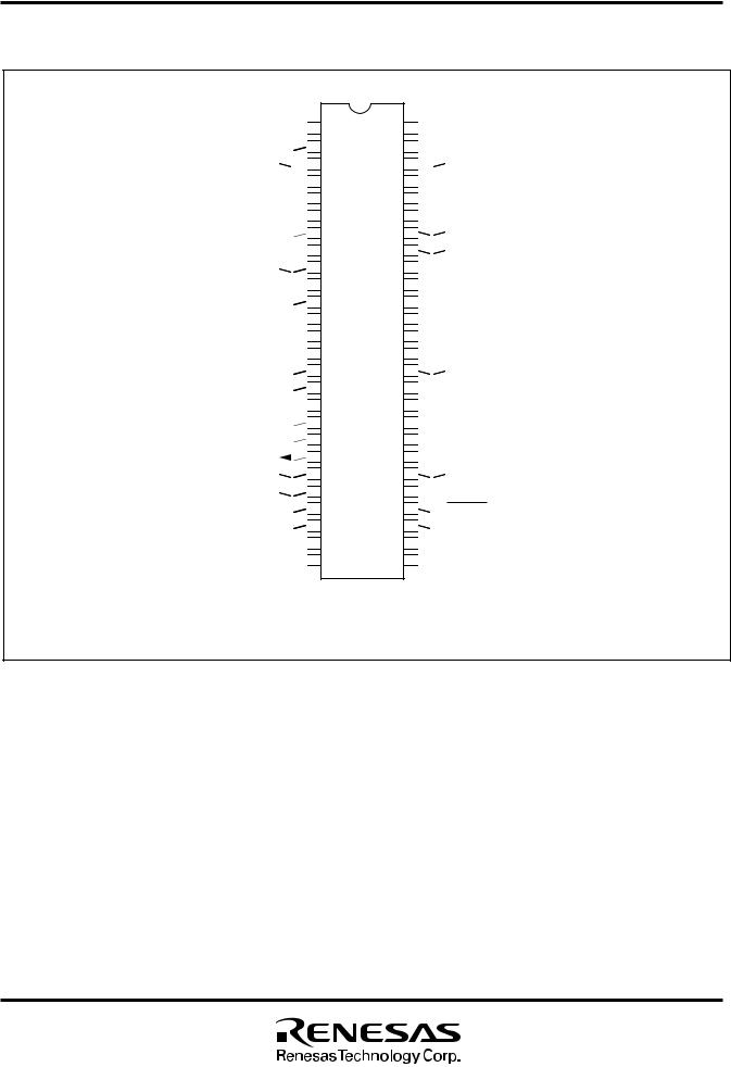
4. PIN CONFIGURATION
HSYNC 
 1
1
VSYNC 
 2
2
P60/PWM0
 3
3
P61/PWM1
 4
4
P62/PWM2
 5
5
P63/PWM3
 6
6
P00/PWM4

 7
7
P01/PWM5

 8
8
P02/PWM6

 9
9
P03/PWM7

 10 P42/SIN/A-D5
 11 P41/SCLK/A-D6

 12
12
P40/SOUT(/IN)/A-D7

 13
13
DA
 14
14
P35/INT2/A-D4 
 15 P34/INT1
 16 P33/TIM3
 17 P32/TIM2
 18
18
P24

 19
19
P25

 20
20
P26

 21
21
P27

 22 CNVSS
 23 XIN
 24
24
XOUT
 25
25
VSS 
 26
26
M37212EFSP XXXSP,-37212M4/M6/M8M
52 
 P52/R
P52/R
51 
 P53/G
P53/G
50 
 P54/B
P54/B
49 
 P55/OUT1
48 

 P20
P20
47 

 P21
P21
46 

 P22
P22
45 

 P23
P23
44 

 P04
P04
43 

 P05
P05
42 

 P06
P06
41 

 P07
P07
40 

 P10/OUT2/A-D8 39

 P11/SCL1
38 

 P12/SCL2
37 

 P13/SDA1
36 

 P14/SDA2
35 
 P15/INT3/A-D1 34
 P16/A-D2
33 
 P17/A-D3
32 

 P30
P30
31 

 P31
P31
30 
 RESET
RESET
29 
 OSC1/P36
28 

 OSC2/P37
27 
 VCC
VCC
Outline 52P4B
Fig. 4.1 Pin Configuration 1 (Top View)
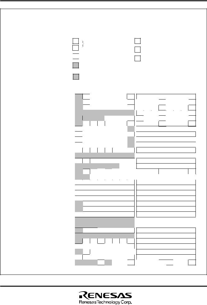
Rev. 1.0
3

MITSUBISHI MICROCOMPUTERS
M37212M4/M8–XXXSP, M37212M6–XXXSP/FP
M37212EFSP/FP
SINGLE-CHIP 8-BIT CMOS MICROCOMPUTER for VOLTAGE SYNTHESIZER with ON-SCREEN DISPLAY CONTROLLER
|
NC |
NC |
NC |
NC |
P22 |
P23 |
P04 |
P05 |
P06 |
P07 |
P10/OUT2/A-D8 |
NC |
P11/SCL1 |
P12/SCL2 |
P13/SDA1 |
P14/SDA2 |
NC |
P15/INT3/A-D1 |
P16/A-D2 |
P17/A-D3 |
NC NC |
NC |
NC |
|
|
|
64 |
63 |
62 |
61 |
60 |
59 |
58 |
57 |
56 |
55 |
54 |
53 |
52 |
51 |
50 |
49 |
48 |
47 |
46 |
45 |
44 |
43 |
42 |
41 |
|
P21 |
65 |
|
|
|
|
|
|
|
|
|
|
|
|
|
|
|
|
|
|
|
|
|
|
40 |
P30 |
NC |
66 |
|
|
|
|
|
|
|
|
|
|
|
|
|
|
|
|
|
|
|
|
|
|
39 |
NC |
P20 |
67 |
|
|
|
|
|
|
|
|
|
|
|
|
|
|
|
|
|
|
|
|
|
|
38 |
P31 |
P55/OUT1 |
68 |
|
|
|
|
|
|
|
|
|
|
|
|
|
|
|
|
|
|
|
|
|
|
37 |
RESET |
P54/B |
69 |
|
|
|
|
|
|
|
|
|
|
|
|
|
|
|
|
|
|
|
|
|
|
36 |
OSC1/P36 |
P53/G |
70 |
|
|
|
|
|
|
|
|
|
|
|
|
|
|
|
|
|
|
|
|
|
|
35 |
OSC2/P37 |
P52/R |
71 |
|
|
|
M37212M6-XXXFP, M37212EFFP |
|
|
|
|
|
34 |
VCC |
|||||||||||||
NC |
72 |
|
|
|
|
|
|
|
|
33 |
NC |
||||||||||||||
NC |
73 |
|
|
|
|
|
|
|
|
|
|
|
|
|
|
|
|
|
|
|
|
|
|
32 |
NC |
HSYNC |
74 |
|
|
|
|
|
|
|
|
|
|
|
|
|
|
|
|
|
|
|
|
|
|
31 |
VSS |
VSYNC |
75 |
|
|
|
|
|
|
|
|
|
|
|
|
|
|
|
|
|
|
|
|
|
|
30 |
XOUT |
P60/PWM0 |
76 |
|
|
|
|
|
|
|
|
|
|
|
|
|
|
|
|
|
|
|
|
|
|
29 |
XIN |
P61/PWM1 |
77 |
|
|
|
|
|
|
|
|
|
|
|
|
|
|
|
|
|
|
|
|
|
|
28 |
CNVSS |
P62/PWM2 |
78 |
|
|
|
|
|
|
|
|
|
|
|
|
|
|
|
|
|
|
|
|
|
|
27 |
P27 |
NC |
|
|
|
|
|
|
|
|
|
|
|
|
|
|
|
|
|
|
|
|
|
|
|
||
79 |
|
|
|
|
|
|
|
|
|
|
|
|
|
|
|
|
|
|
|
|
|
|
26 |
NC |
|
P63/PWM3 |
80 |
|
|
|
|
|
|
|
|
|
|
|
|
|
|
|
|
|
|
|
|
|
|
25 |
NC |
|
1 |
2 |
3 |
4 |
5 |
6 |
7 |
8 |
9 |
10 |
11 |
12 |
13 |
14 |
15 |
16 |
17 |
18 |
19 |
0 |
21 |
22 |
23 |
24 |
|
|
2 |
|
|||||||||||||||||||||||
|
NC |
NC |
NC |
NC |
P00/PWM4 |
P01/PWM5 |
P02/PWM6 |
P03/PWM7 |
NC |
P42/SIN/A-D5 |
P41/SCLK/A-D6 |
P40/SOUT(/IN)/A-D7 |
DA |
P35/INT2/A-D4 |
P34/INT1 |
P33/TIM3 |
P32/TIM2 |
4 |
P25 |
P26 |
NC |
NC |
NC |
NC |
|
|
2 |
|
|||||||||||||||||||||||
|
P |
|
|||||||||||||||||||||||
|
|
|
|||||||||||||||||||||||
|
|
|
|
|
|
|
|
Outline 80P6N-A |
|
|
|
|
|
|
|
|
NC : Unconnected |
||||||||
Fig. 4.2 Pin Configuration 2 (Top View)
Rev. 1.0
4

MITSUBISHI MICROCOMPUTERS
M37212M4/M8–XXXSP, M37212M6–XXXSP/FP
M37212EFSP/FP
SINGLE-CHIP 8-BIT CMOS MICROCOMPUTER for VOLTAGE SYNTHESIZER with ON-SCREEN DISPLAY CONTROLLER
5. FUNCTIONAL BLOCK DIAGRAM
|
|
|
|
|
|
|
|
|
|
|
5 |
|
|
|
|
|
|
|
|
|
|
SYNC |
|
Output ports P60–P63 Output ports P52–P5 |
|
|
|
|
|
|
|
|
|
|
H |
|
|
|
|
|
|
|
|
|
|
|
|
SYNC |
|
|
|
|
|
|
|
|
|
|
|
|
V |
|
|
|
|
|
|
|
|
|
|
|
|
R |
|
|
|
|
|
|
|
|
|
|
|
|
G |
|
|
|
|
|
|
|
|
|
|
|
|
B |
|
|
|
|
|
|
|
|
|
|
|
|
OUT1 |
|
|
|
|
|
|
|
|
|
|
|
|
OUT2 |
|
|
|
Input ports P36,P37 |
input for display Clockdisplayoutputfor |
OSC1 OSC2 |
29 28 |
|
|
circuit P6 (4) P5(4) |
PWM0 |
6 5 4 3 5051524921 |
|
displayOutputfor |
||
|
|
PWM1 |
|
|||||||||
|
|
PWM2 |
|
|||||||||
|
Clock |
|
|
|
|
bit PWM |
PWM3 |
|
|
|
|
|
|
|
|
|
|
PWM4 |
|
|
|
|
|||
|
|
|
|
|
PWM5 |
|
|
|
|
|||
|
|
|
|
|
PWM6 |
|
|
|
|
|||
|
|
|
|
|
|
8- |
PWM7 |
|
|
|
|
|
|
|
|
|
|
|
SI/O(8) |
OUT(/IN) |
S |
|
P40, P41 |
|
|
|
|
|
|
|
|
|
|
|
||||
|
|
|
|
|
|
CLK |
S |
|
|
|||
|
|
|
|
|
|
|
|
|
||||
|
|
|
|
|
|
IN |
S |
|
|
|||
|
|
|
|
|
|
|
|
|
||||
|
|
|
|
|
|
|
|
|
|
|||
|
|
|
|
|
|
|
|
P4 (3) |
1112 13 |
2 |
I/O ports |
|
|
|
|
|
|
|
|
|
|
|
P4 |
|
|
|
|
|
|
|
|
Multi-master |
C-BUS interface |
SCL |
|
Input port |
, P31 |
|
|
|
|
|
|
|
SDA |
|
|
||||
|
|
|
|
|
|
|
|
|
||||
|
|
|
|
|
|
|
2 |
|
|
|
P30 |
|
|
|
|
|
|
|
|
I |
|
|
|
|
|
|
|
VCC VSS CNVSS |
27 26 23 |
|
|
|
|
P3 (6) |
14 15161718 3132 |
DA I/O ports |
Input ports P32–P35 |
|
|
|
|
|
14-bit |
PWM circuit |
INT1 |
||||||
|
|
|
|
INT2 |
||||||||
|
Clock input Clock output Reset input |
|
|
|
|
|
|
INT3 |
4142434410 9 8 7 3334353637383940 2221201945464748 |
|
|
|
|
RESET |
24 25 30 |
|
|
|
|
P0 (8) P1 (8) P2 (8) |
|
|
Input ports P15–P17 I/O port P2 |
||
|
Timing output |
|
Data bus |
A-D |
comparator |
|
I/O port P0 I/O ports P10–P14 |
|||||
|
) |
|
|
|
||||||||
|
( |
|
generating |
|
||||||||
|
XIN XOUT |
Clock |
|
|||||||||
Fig. 5.1 Functional Block Diagram of M37212 |
|
|
|
|
|
|
|
|||||
Rev. 1.0
5

MITSUBISHI MICROCOMPUTERS
M37212M4/M8–XXXSP, M37212M6–XXXSP/FP
M37212EFSP/FP
SINGLE-CHIP 8-BIT CMOS MICROCOMPUTER for VOLTAGE SYNTHESIZER with ON-SCREEN DISPLAY CONTROLLER
6. PERFORMANCE OVERVIEW
Table 6.1 Performance Overview
Parameter |
|
|
Functions |
|
Number of basic instructions |
|
|
|
71 |
|
|
|
|
|
Number of basic instructions |
|
|
|
0.5 μs (the minimum instruction execution time, at 8 MHz oscillation fre |
|
|
|
|
quency) |
Instruction execution time |
|
|
|
8 MHz (maximum) |
Memory size |
ROM |
M37212M4-XXXSP |
16K bytes |
|
|
|
M37212M6-XXXSP/FP |
24K bytes |
|
|
|
|
|
|
|
|
M37212M8-XXXSP |
32K bytes |
|
|
|
|
|
|
|
|
M37212EFSP/FP |
62K bytes |
|
|
|
|
|
|
|
RAM |
M37212M4-XXXSP |
320 bytes |
|
|
|
M37212M6-XXXSP/FP |
384 bytes |
|
|
|
M37212M8-XXXSP |
576 bytes (ROM correction memory included) |
|
|
|
M37212EFSP/FP |
1280 bytes (ROM correction memory included) |
|
|
OSD ROM |
|
8 K bytes |
|
|
|
|
|
|
|
OSD RAM |
|
96 bytes |
|
|
|
|
|
|
Input/Output ports |
P0 |
|
I/O |
8-bit 1 (N-channel open-drain output structure, can be used as PWM |
|
|
|
|
output pins) |
|
P10–P14 |
I/O |
5-bit 1 (CMOS input/output output structure, however, N-channel open- |
|
|
|
|
|
drain output structure, when P11–P14 are used as multi-master I2C-BUS |
|
|
|
|
interface, can be used as OSD output, A-D input, multi-master I2C-BUS |
|
|
|
|
interface) |
|
P15–P17 |
Input |
3-bit 1 (can be used as INT input pin, A-D input pins) |
|
|
|
|
|
|
|
P20–P27 |
I/O |
8-bit 1 (CMOS input/output structure) |
|
|
|
|
|
|
|
P30, P31 |
I/O |
2-bit 1 (CMOS input/output structure) |
|
|
|
|
|
|
|
P32–P37 |
Input |
6-bit 1 (can be used as external clock input pins, INT input pins, OSD |
|
|
|
|
|
display clock I/O pins, A-D input pins) |
|
P40, P41 |
I/O |
2-bit 1 (N-channel open-drain output structure, can be used as serial I/O |
|
|
|
|
|
pins, A-D input pins) |
|
|
|
|
|
|
P42 |
|
Input |
1-bit 1(can be used as serial input pin, A-D input pin) |
|
|
|
|
|
|
P52–P55 |
Output |
4-bit 1 (CMOS output structure, can be used as OSD output pins) |
|
|
|
|
|
|
|
P60–P63 |
Output |
4-bit 1 (N-channel open-drain output structure, can be used as PWM |
|
|
|
|
|
output pins) |
Serial I/O |
|
|
|
8-bit 1 |
Multi-master I2C-BUS interface |
|
|
|
1 (2 systems) |
A-D comparator |
|
|
|
8 channels (6-bit resolution) |
|
|
|
|
|
PWM output circuit |
|
|
|
14-bit 1, 8-bit 8 |
|
|
|
|
|
Timers |
|
|
|
8-bit timer 4 |
Subroutine nesting |
|
|
|
96 levels (maximum) |
Interrupt |
|
|
|
<14 sources> |
|
|
|
|
INT external interrupt 3, Internal timer interrupt 4, Serial I/O interrupt 1, |
|
|
|
|
OSD interrupt 1, Multi-master I2C-BUS interface interrupt 1, f(XIN)/4096 |
|
|
|
|
interrupt 1, VSYNC interrupt 1, BRK interrupt 1, Reset 1 |
Clock generating circuit |
|
|
|
2 built-in circuits (externally connected a ceramic resonator or a quartz- |
|
|
|
|
crystal oscillator) |
|
|
|
|
|
Rev. 1.0
6

MITSUBISHI MICROCOMPUTERS
M37212M4/M8–XXXSP, M37212M6–XXXSP/FP
M37212EFSP/FP
SINGLE-CHIP 8-BIT CMOS MICROCOMPUTER for VOLTAGE SYNTHESIZER with ON-SCREEN DISPLAY CONTROLLER
Table 6.2 Performance Overview (continued)
|
Parameter |
Functions |
|
OSD display |
Number of display characters |
24 characters 2 lines |
|
function |
Dot structure |
12 16 dots |
|
|
|||
|
Kinds of characters |
254 kinds |
|
|
|
|
|
|
Kinds of character sizes |
3 kinds |
|
|
|
|
|
|
Character font coloring |
1 screen: 8 kinds (per character unit) |
|
|
|
|
|
|
Display position |
Horizontal: 64 levels, Vertical: 128 levels |
|
Power source voltage |
5 V ± 10 % |
||
Power dissipation |
|
OSD ON |
165 mW typ. (at oscillation frequency f(XIN) = 8 MHz, fOSC = 8 MHz) |
|
|
OSD OFF |
110 mW typ. (at oscillation frequency f(XIN) = 8 MHz) |
|
|
In stop mode |
1.65 mW (maximum) |
Operating temperature range |
–10 °C to 70 °C |
||
Device structure |
|
|
CMOS silicon gate process |
|
|
|
|
Package |
M37212M4/M6/M8-XXXSP, M37212EFSP |
52-pin plastic molded SDIP |
|
|
|
|
|
|
M37212M6-XXXFP, M37212EFSP |
80-pin plastic molded QFP |
|
|
|
|
|
Rev. 1.0
7

MITSUBISHI MICROCOMPUTERS
M37212M4/M8–XXXSP, M37212M6–XXXSP/FP
|
|
|
M37212EFSP/FP |
|
|
|
|
SINGLE-CHIP 8-BIT CMOS MICROCOMPUTER for VOLTAGE SYNTHESIZER |
|
|
|
|
with ON-SCREEN DISPLAY CONTROLLER |
|
|
|
|
|
|
7. PIN DESCRIPTION |
|
|
||
Table 7.1 Pin Description |
|
|
||
|
|
|
|
|
Pin |
Name |
Input/ |
Functions |
|
Output |
||||
|
|
|
||
VCC, |
Power source |
|
Apply voltage of 5 V ± 10 % to (typical) VCC, and 0 V to VSS. |
|
VSS. |
|
|
|
|
CNVSS |
CNVSS |
|
This is connected to VSS. |
|
______ |
|
|
To enter the reset state, the reset input pin must be kept at a “L” for 2 μs or more (under |
|
RESET |
Reset input |
Input |
||
|
|
|
normal VCC conditions). |
|
|
|
|
If more time is needed for the quartz-crystal oscillator to stabilize, this “L” condition should |
|
|
|
|
be maintained for the required time. |
|
XIN |
Clock input |
Input |
This chip has an internal clock generating circuit. To control generating frequency, an |
|
|
|
|
external ceramic resonator or a quartz-crystal oscillator is connected between pins XIN and |
|
XOUT |
Clock output |
Output |
XOUT. If an external clock is used, the clock source should be connected to the XIN pin and |
|
|
|
|
the XOUT pin should be left open. |
|
|
|
|
|
|
P00/PWM4– |
I/O port P0 |
I/O |
Port P0 is an 8-bit I/O port with direction register allowing each I/O bit to be individually |
|
P03/PWM7, |
|
|
programmed as input or output. At reset, this port is set to input mode. The output structure |
|
P04–P07 |
|
|
is N-channel open-drain output. (See note) |
|
|
PWM output |
Output |
Pins P00–P03 are also used as PWM output pins PWM4–PWM7 respectively. The output |
|
|
|
|
structure is N-channel open-drain output. |
|
|
|
|
|
|
P10/OUT2/ |
I/O port P1 |
I/O |
Port P10–P14 are a 5-bit I/O port and has basically the same functions as port P0. The |
|
A-D8, |
|
|
output structure is CMOS output. |
|
P11/SCL1, |
OSD output |
Output |
Pins P10 is also used as OSD output pin OUT2. The output structure is CMOS output. |
|
P12/SCL2, |
Multi-master |
I/O |
Pins P11–P14 are used as SCL1, SCL2, SDA1 and SDA2 respectively, when multi-master |
|
P13/SDA1, |
I2C-BUS interface |
|
I2C-BUS interface is used. The output structure is N-channel open-drain output. |
|
P14/SDA2, |
Analog input |
Input |
P10 pin is also used as analog input pin A-D8. |
|
|
|
|
|
|
P15/INT3/ |
Input port P1 |
Input |
Port P15–P17 are a 3-bit input port and has basically the same functions as port P0. |
|
A-D1, |
Analog input |
Input |
Pins P15–P17 are also used as analog input pins A-D1 to A-D3 respectively. |
|
P16/A-D2, |
External interrupt |
Input |
P15 pin is also used as INT external interrupt input pin INT3. |
|
P17/A-D3 |
input |
|
|
|
|
|
|
|
|
P20–P27 |
I/O port P2 |
I/O |
Port P2 is an 8-bit I/O port and has basically the same functions as port P0. The output |
|
|
|
|
structure is CMOS output. (See note) |
|
P30, P31 |
I/O port P3 |
I/O |
Ports P30, P31 are a 2-bit I/O port and has basically the same functions as port P0. The |
|
|
|
|
output structure is CMOS output. |
|
|
|
|
|
|
P32/TIM2, |
Input port P3 |
Input |
Ports P32–P37 are a 6-bit input port and has basically the same functions as port P0. |
|
|
|
|
|
|
P33/TIM3, |
External clock input |
Input |
Pins P32, P33 are also used as external clock input pins TIM2, TIM3 respectively. |
|
|
|
|
|
|
P34/INT1, |
External interrupt |
Input |
Pins P34, P35 are also used as INT external interrupt input pins INT1, INT2 respectively. |
|
P35/INT2/ |
input |
|
|
|
|
|
|
||
A-D4, |
Analog input |
Input |
P35 pin is also used as analog input pin A-D4. |
|
P36/OSC1, |
Clock input for |
Input |
P36 pin is also used as OSD display clock input pin OSC1. |
|
P37/OSC2 |
OSD display |
|
|
|
|
|
|
||
|
|
|
|
|
|
Clock output for |
Output |
P37 pin is also used as OSD display clock output pin OSC2. The output structure is CMOS |
|
|
OSD display |
|
output. |
|
|
|
|
|
|
Rev. 1.0
8

MITSUBISHI MICROCOMPUTERS
M37212M4/M8–XXXSP, M37212M6–XXXSP/FP
M37212EFSP/FP
SINGLE-CHIP 8-BIT CMOS MICROCOMPUTER for VOLTAGE SYNTHESIZER with ON-SCREEN DISPLAY CONTROLLER
Table 7.2 Pin Description (continued)
Pin |
Name |
Input/ |
Functions |
|
Output |
||||
|
|
|
||
P40/SOUT(/IN)/ |
I/O port P4 |
I/O |
Ports P40, P41 are a 2-bit I/O port and has basically the same functions as port P0. The |
|
A-D7, |
|
|
output structure is N-channel open-drain output. |
|
P41/SCLK/ |
Serial I/O data |
I/O |
Pin P40 is also used as serial I/O data input/output pin SOUT(/IN). The output structure is N- |
|
A-D6, |
input/output |
|
channel open-drain output. |
|
|
|
|
|
|
|
Serial I/O synchronizing |
I/O |
Pin P41 is also used as serial I/O synchronizing clock input/output pin SCLK. The output |
|
|
clock input/output |
|
structure is N-channel open-drain output. |
|
|
Analog input pin |
Input |
Pin P40, P41 are also used as analog input pins A-D7, A-D6 respectively. |
|
P42/SIN/ |
Input port P4 |
Input |
Port P42 is a 1-bit input port and has basically the same functions as port P0. |
|
|
|
|
|
|
A-D5, |
Serial I/O data |
Input |
Pin P42 is also used as serial I/O data input pin SIN. |
|
|
input |
|
|
|
|
|
|
|
|
|
Analog input |
Input |
Pin P42 is also used as analog input pin A-D5. |
|
P52/R, |
Output port P5 |
Output |
Ports P52–P55 are a 4-bit output port and has basically the same functions as port P0. The |
|
P53/G, |
|
|
output structure is CMOS output. |
|
P54/B, |
OSD output |
Output |
Pins P52–P55 are also used as OSD output pins R, G, B, OUT1 respectively. The output |
|
P55/OUT1 |
|
|
structure is CMOS output. |
|
P60PWM0– |
Output port P6 |
Output |
Ports P60–P63 are a 4-bit I/O port and has basically the same functions as port P0. The |
|
P63/PWM3 |
|
|
output structure is N-channel open-drain output. |
|
|
PWM output |
Output |
Pins P60–P63 are also used as PWM output pins PWM0–PWM3 respectively. The output |
|
|
|
|
structure is N-channel open-drain output. |
|
|
|
|
|
|
HSYNC |
HSYNC input |
Input |
This is a horizontal synchronizing signal input for OSD. |
|
VSYNC |
VSYNC input |
Input |
This is a vertical synchronizing signal input for OSD. |
|
DA |
DA output |
Output |
This is a 14-bit PWM output pin. |
|
|
|
|
|
Note : Port Pi (i = 0 to 3) has the port Pi direction register which can be used to program each bit as an input (“0”) or an output (“1”). The pins programmed as “1” in the direction register are output pins. When pins are programmed as “0,” they are input pins. When pins are programmed as output pins, the output data are written into the port latch and then output. When data is read from the output pins, the output pin level is not read but the data of the port latch is read. This allows a previously-output value to be read correctly even if the output “L” voltage has risen, for example, because a light emitting diode was directly driven. The input pins are in the floating state, so the values of the pins can be read. When data is written into the input pin, it is written only into the port latch, while the pin remains in the floating state.
Rev. 1.0
9
MITSUBISHI MICROCOMPUTERS
M37212M4/M8–XXXSP, M37212M6–XXXSP/FP M37212EFSP/FP
SINGLE-CHIP 8-BIT CMOS MICROCOMPUTER for VOLTAGE SYNTHESIZER with ON-SCREEN DISPLAY CONTROLLER
Port P0
Data bus
Ports P10, P2, P30, P31
Data bus
Ports P40, P41
Data bus
Ports P11–P14
Data bus
I2C-BUS clock
I2C-BUS data
|
N-channel open-drain output |
Direction register |
|
|
Port P0 |
Port latch |
Note : Each port is also used as follows : |
|
P00–P03 : PWM4–PWM7 |
Direction register
CMOS output
Ports P10, P2, P30, P31
Port latch
Note : Port P10 is also used as OUT2/
A-D8.
SIN, SCLK
|
|
|
N-channel open-drain output |
||
Direction register |
|
|
|
|
|
|
|
|
Ports P40, P41 |
||
|
|
|
|||
Port latch |
|
|
Note : Each port is also used as follows : |
||
|
|
||||
|
|
||||
|
|
||||
|
|
P40 |
: SOUT(/IN)/A-D7 |
||
|
|
|
|||
|
|
|
P41 |
: SCLK/A-D6 |
|
SCL1, SCL2,
BSEL0 SDA1, SDA2
BSEL1 
N-channel open-drain output
Direction register
CMOS output
Ports P11–P14
Port latch
Notes 1: Each port is also used as follows : P11 : SCL1
P12 : SCL2
P13 : SDA1
P14 : SDA2
2: The output structure of ports P11– P14 is N-channel open-drain output when using as multi-master I2C- BUS interface (it is the same with ports P40 and P41).
Fig. 7.1 I/O Pin Block Diagram (1)
Rev. 1.0
10

MITSUBISHI MICROCOMPUTERS
M37212M4/M8–XXXSP, M37212M6–XXXSP/FP M37212EFSP/FP
SINGLE-CHIP 8-BIT CMOS MICROCOMPUTER for VOLTAGE SYNTHESIZER with ON-SCREEN DISPLAY CONTROLLER
PortsP16, P17
Data bus
PortsP15, P32–P37, P42
TIM2, TIM3,
INT1,
INT2, SIN, INT3
Data bus 

Ports P60–P63 |
|
Data bus |
Port latch |
D-A, R, G, B, OUT1 , OUT2
Internal circuit 
Ports P16, P17
Note : Each port is also used as follows : P16 : A-D2
P17 : A-D3
Schmidt input
Ports P15, P32–P37, P42
Note : Each port is also used as follows : P15 : INT3/A-D1
P32 : TIM2
P33 : TIM3
P34 : INT1
P35 : INT2/A-D4
P36 : OSC1
P37 : OSC2
P42 : SIN/A-D5
N-chanel open drain output
Ports P60–P63
Note : Each port is also used as follows : P60–P63 : PWM0–PWM3
CMOS output
Ports D-A, R, G, B, OUT1, OUT2
Note : Each pin is also used as follows : R : P52
G : P53
B : P54 OUT1 : P55
OUT2 : P10/A-D8
HSYNC, VSYNC
Schmidt input
Internal circuit |
Ports HSYNC, VSYNC |
Fig. 7.2 I/O Pin Block Diagram (2)
Rev. 1.0
11

MITSUBISHI MICROCOMPUTERS
M37212M4/M8–XXXSP, M37212M6–XXXSP/FP M37212EFSP/FP
SINGLE-CHIP 8-BIT CMOS MICROCOMPUTER for VOLTAGE SYNTHESIZER with ON-SCREEN DISPLAY CONTROLLER
8. FUNCTIONAL DESCRIPTION
8.1 CENTRAL PROCESSING UNIT (CPU)
This microcomputer uses the standard 740 Family instruction set. Refer to the table of 740 Family addressing modes and machine instructions or the SERIES 740 <Software> User’s Manual for details on the instruction set.
Machine-resident 740 Family instructions are as follows:
The FST, SLW instruction cannot be used.
The MUL, DIV, WIT and STP instructions can be used.
8.1.1 CPU Mode Register
The CPU mode register contains the stack page selection bit and internal system clock selection bit. The CPU mode register is allocated at address 00FB16.
CPU Mode Register
b7b6 b5b4b3 b2b1b0 |
|
|
|
|
|
|||||||||
1 |
1 |
1 |
1 |
1 |
|
0 |
0 |
|
|
|
|
|
||
|
CPU mode register (CM) [Address 00FB16] |
|
|
|||||||||||
|
|
|
|
|
|
|
|
|
|
|
|
|
|
|
|
|
|
|
|
|
|
|
B |
Name |
Functions |
After reset |
R W |
||
|
|
|
|
|
|
|
|
|
|
|
|
|
|
|
|
|
|
|
|
|
|
|
0, 1 |
Fix these bits to “0.” |
|
|
Indeterminate R W |
||
|
|
|
|
|
|
|
|
|
|
|
|
|
||
|
|
|
|
|
|
|
|
2 |
Stack page selection |
0: 0 page |
1 |
R W |
||
|
|
|
|
|
|
|
|
|
|
bit (CM2) (See note) |
1: 1 page |
|
|
|
|
|
|
|
|
|
|
|
|
|
|
|
|
|
|
|
|
|
|
|
|
|
|
3 to 7 |
Fix these bits to “1.” |
|
|
Indeterminate R W |
||
|
|
|
|
|
|
|
|
|
|
|
|
|
|
|
Note: This bit is set to “1” after the reset release.
Fig. 8.1.1 CPU Mode Register
Rev. 1.0
12

MITSUBISHI MICROCOMPUTERS
M37212M4/M8–XXXSP, M37212M6–XXXSP/FP M37212EFSP/FP
SINGLE-CHIP 8-BIT CMOS MICROCOMPUTER for VOLTAGE SYNTHESIZER with ON-SCREEN DISPLAY CONTROLLER
8.2 MEMORY
8.2.1 Special Function Register (SFR) Area
The special function register (SFR) area in the zero page contains control registers such as I/O ports and timers.
8.2.2 RAM
RAM is used for data storage and for stack area of subroutine calls and interrupts.
8.2.7 Zero Page
The 256 bytes from addresses 000016 to 00FF16 are called the zero page area. The internal RAM and the special function registers (SFR) are allocated to this area.
The zero page addressing mode can be used to specify memory and register addresses in the zero page area. Access to this area with only 2 bytes is possible in the zero page addressing mode.
8.2.3 ROM
ROM is used for storing user programs as well as the interrupt vector area.
8.2.4 OSD RAM
RAM for display is used for specifying the character codes and colors to display.
8.2.8 Special Page
The 256 bytes from addresses FF0016 to FFFF16 are called the special page area. The special page addressing mode can be used to specify memory addresses in the special page area. Access to this area with only 2 bytes is possible in the special page addressing mode.
8.2.5 OSD ROM |
8.2.9 ROM Correction Memory (RAM) |
This is used as the program area for ROM correction. |
|
ROM for display is used for storing character data. |
|
|
Note: Only M37212M8-XXXSP and M37212EFSP/FP have ROM correction |
8.2.6 Interrupt Vector Area |
memory. |
|
|
The interrupt vector area contains reset and interrupt vectors. |
|
■ M37212M4/M8-XXXSP, M37212M6-XXXSP/FP
|
|
|
|
000016 |
|
1000016 |
|
|
|
|
|
||
|
|
|
|
|
|
OSD ROM |
|
|
|
|
|
|
(8K bytes) |
|
M37212M6- |
00BF16 |
|
|||
|
|
Zero page |
||||
|
XXXSP/FP |
|
00C016 |
SFR area |
11FFF16 |
|
|
RAM |
00FF16 |
||||
|
|
|
||||
|
(384 bytes) |
010016 |
|
|
||
|
|
|
||||
M37212M4- |
|
|
|
|||
XXXSP |
017F16 |
|
|
|||
RAM |
|
|
||||
|
|
|
||||
(320 bytes) |
01BF16 |
|
|
|||
|
|
|
Not used |
||
|
|
|
|
|
Not used |
OSD RAM |
060016 |
|
|
|
|
|
|
|
|||
(96 bytes) |
|
|
|
|
|
(See note) |
06B716 |
|
|
|
|
|
|
|
|
|
|
M37212M6- |
|
Not used |
|
|
|
|
|
|
|
||
XXXSP/FP |
|
|
|
|
|
ROM |
|
A00016 |
|
|
|
(24K bytes) |
|
|
|
||
M37212M4- |
C00016 |
|
|
|
|
|
|
|
|||
|
|
|
|
||
XXXSP |
|
|
|
|
|
ROM |
|
|
|
|
|
(16K bytes) |
|
|
|
|
|
|
|
FF0016 |
|
|
|
|
|
|
|
|
|
|
|
FFDE16 |
|
Special page |
|
|
|
|
|||
|
|
FFFF16 |
Interrupt vector area |
||
|
|
|
1FFFF16 |
|
|
|
|
|
|
||
|
|
|
|
Note: Refer to Table 8.10.3 OSD RAM. |
|
Fig. 8.2.1 Memory Map (M37212M4/M8-XXXSP, M37212M6-XXXSP/FP)
Rev. 1.0
13

MITSUBISHI MICROCOMPUTERS
M37212M4/M8–XXXSP, M37212M6–XXXSP/FP
M37212EFSP/FP
SINGLE-CHIP 8-BIT CMOS MICROCOMPUTER for VOLTAGE SYNTHESIZER with ON-SCREEN DISPLAY CONTROLLER
■ M37212M8-XXXSP, M37212EFSP/FP
|
|
|
|
|
|
|
|
|
|
000016 |
|
1000016 |
|
|||
|
|
|
|
|
|
|
|
|
|
|
|
|||||
|
|
|
|
|
|
|
|
|
|
|
|
|
|
OSD ROM |
||
|
|
|
|
|
|
|
|
|
|
|
00BF16 |
|
|
(8K bytes) |
||
|
|
|
|
|
|
|
|
|
|
|
|
Zero page |
||||
|
|
|
|
|
|
|
|
|
|
|
00C016 |
SFR area |
|
|
11FFF16 |
|
|
|
|
|
|
|
|
|
|
|
|
00FF16 |
|
|
|||
|
|
|
|
|
|
|
|
|
|
|
|
|
|
|
|
|
|
|
|
|
M37212M8- |
|
|
|
|
|
|
|
|||||
|
|
|
|
|
|
010016 |
|
|
|
|
|
|||||
M37212EFSP |
|
|
|
|
|
|||||||||||
|
XXXSP |
|
|
|
|
|
|
|
||||||||
RAM |
|
|
|
|
|
|
|
|
|
|
|
|||||
|
|
|
RAM |
|
|
|
|
|
|
|
|
|
||||
(1280 bytes) |
|
|
|
|
|
|
|
|
|
|
|
|||||
|
(576 bytes) |
|
|
|
01FF16 |
|
|
|
|
|
||||||
|
|
|
|
|
|
|
|
|
|
|
|
|||||
|
|
|
|
|
|
|
|
|
||||||||
|
|
|
|
|
|
|
|
|
|
|
|
|
|
|
|
|
|
|
|
|
|
|
|
|
|
|
|
|
|
|
|
|
|
|
|
|
|
|
|
|
|
|
|
Not used |
|
|
|
|
||
|
|
|
|
|
|
|
|
|
|
|
|
|
|
|
|
|
|
|
|
|
|
|
|
|
|
|
021716 |
|
|
|
|
|
|
|
|
|
|
|
|
|
|
|
|
2 page register |
|
|
|
|
||
|
|
|
|
|
|
|
|
|
|
|
021B16 |
|
|
|
|
|
|
|
|
|
|
|
|
|
|
|
|
|
|
|
|
||
|
|
|
|
|
|
|
|
|
|
|
|
|
|
|
|
|
|
|
|
|
|
|
|
|
|
|
|
|
Not used |
|
|
|
|
|
|
|
|
|
|
|
|
|
|
|
02C016 |
|
|
|
|
|
|
|
|
|
|
|
|
|
|
|
|
|
ROM correction function |
|
|
||
|
|
|
|
|
|
|
|
|
|
|
|
|
|
|
|
|
|
|
|
|
|
|
|
|
|
|
|
02E016 |
|
|
Vector 1: address 02C016 |
|
|
|
|
|
|
|
|
|
|
|
|
|
033F16 |
|
|
Vector 2: address 02E016 |
|
|
|
|
|
|
|
|
|
|
|
|
|
|
|
|
|
|
|
|
|
|
|
|
|
|
|
|
|
|
|
|
|
|
|
|
|
|
|
|
|
|
|
|
|
|
|
05FF16 |
|
|
|
|
Not used |
|
|
|
|
|
|
|
|
|
|
|
|
|
|
|
||
|
|
|
|
OSD RAM |
060016 |
|
|
|
|
|||||||
|
|
|
|
|
|
|
|
|
||||||||
|
|
|
|
|
|
|
|
|
|
|
||||||
|
|
|
|
(96 bytes) |
|
|
|
|
|
|
|
|||||
|
|
|
|
(See note) |
|
|
|
|
|
|
|
|||||
|
|
|
|
|
|
|
|
|
|
|
06B716 |
|
|
|
|
|
|
M37212EFSP |
|
|
Not used |
|
|
|
|
||||||||
|
080016 |
|
|
|
|
|
||||||||||
|
|
ROM |
|
|
|
|
|
|||||||||
|
|
|
|
|
|
|
|
|
||||||||
|
|
(62K bytes) |
|
|
|
|
800016 |
|
|
|
|
|
||||
|
|
|
|
|
|
|
|
|
|
|
|
|
|
|
||
M37212M8-
XXXSP
ROM (32K bytes)
FF0016 |
|
|
FFDE16 |
Special page |
|
FFFF16 |
Interrupt vector area |
|
1FFFF16 |
||
|
||
|
Note: Refer to Table 8.10.3 OSD RAM |
Fig. 8.2.2 Memory Map (M37212M8-XXXSP, M37212EFSP/FP)
Rev. 1.0
14

MITSUBISHI MICROCOMPUTERS
M37212M4/M8–XXXSP, M37212M6–XXXSP/FP
M37212EFSP/FP
SINGLE-CHIP 8-BIT CMOS MICROCOMPUTER for VOLTAGE SYNTHESIZER with ON-SCREEN DISPLAY CONTROLLER
■ SFR area (addresses C016 to DF16)
Address
C016
C116
C216
C316
C416
C516
C616
C716
C816
C916
CA16
CB16
CC16
CD16
CE16
CF16
D016
D116
D216
D316
D416
D516
D616
D716
D816
D916
DA16
DB16
DC16
DD16
DE16
DF16
Register
Port P0 (P0)
Port P0 direction register (D0) Port P1 (P1)
Port P1 direction register (D1) Port P2 (P2)
Port P2 direction register (D2) Port P3 (P3)
Port P3 direction register (D3) Port P4 (P4)
Port P4 direction register (D4) Port P5 (P5)
Port P5 direction register (D5) Port P6 (P6)
DA-H register (DA-H)
DA-L register (DA-L)
PWM0 register (PWM0)
PWM1 register (PWM1)
PWM2 register (PWM2)
PWM3 register (PWM3)
PWM4 register (PWM4)
PWM output control register 1 (PW) PWM output control register 2 (PN) I2C data shift register (S0)
I2C address register (S0D) I2C status register (S1) I2C control register (S1D)
I2C clock control register (S2) Serial I/O mode register (SM) Serial I/O register (SIO)
Bit allocation
:
Function bit
Name :

 : No function bit
0: Fix to this bit to “0” (do not write to “1”)
1: Fix to this bit to “1” (do not write to “0”)
Bit allocation
b7 |
|
|
|
|
|
|
b0 |
|
|
|
|
|
|
|
|
|
|
|
|
|
|
|
|
|
|
|
|
|
|
|
|
|
|
|
|
|
|
|
|
|
|
|
|
|
|
|
|
|
|
|
|
|
|
|
|
|
|
|
|
|
|
|
|
|
|
|
|
|
|
P31D |
P30D |
|
|
|
|
|
|
|
|
|
|
|
|
|
|
P41 |
P40 |
|
|
|
|
|
|
|
|
|
|
|
|
|
|
P41D |
P40D |
|
|
|
|
|
|
|
|
|
|
P55 |
P54 |
P53 |
P52 |
|
|
|
|
P55 |
P54 |
P53 |
P52 |
0 |
0 |
|
|
SEL |
SEL |
SEL |
SEL |
|
|
|
|
|
|
P63 |
P62 |
P61 |
P60 |
|
|
|
|
|
|
|
|
|
|
|
|
1 |
1 |
1 |
1 |
|
|
|
|
|
|
|
|
|
|
|
|
|
|
|
|
|
|
|
|||||
|
|
|
|||||
|
|
|
|||||
|
|
|
|||||
|
|
|
|||||
PW7 |
PW6 |
PW5 |
PW4 |
PW3 |
PW2 |
PW1 |
PW0 |
|
|
|
|
|
|
|
|
|
|
|
PN4 |
PN3 |
PN2 |
PN1 |
PN0 |
D7 |
D6 |
D5 |
D4 |
D3 |
D2 |
D1 |
D0 |
|
|
|
|
|
|
|
|
SAD6 |
SAD5 |
SAD4 |
SAD3 |
SAD2 |
SAD1 |
SAD0RBW |
|
|
|
|
|
|
|
|
|
MST |
TRX |
BB |
PIN |
AL |
AAS |
AD0 LRB |
|
|
|
|
|
|
|
|
|
BSEL1 |
BSEL0 |
10BIT |
ALS |
ESO |
BC2 |
BC1 BC0 |
|
|
|
SAD |
|
|
|
|
|
ACK |
ACK |
FAST |
CCR4 |
CCR3 |
CCR2 |
CCR1 CCR0 |
|
|
BIT |
MODE |
|
|
|
|
|
|
SM6 |
SM5 |
0 |
SM3 |
SM2 |
SM1 SM0 |
|
|
|
|
|
|
|
|
|
|
|
|
|
|
|
|
|
|
|
|
|
|
|
|
|
State immediately after reset
0: “0” immediately after reset
1: “1” immediately after reset
?: Indeterminate immediately after reset
State immediately after reset
|
b7 |
|
|
|
|
|
|
|
b0 |
|
|
|
|
|
|
? |
|
|
|
|
|
|
|
|
|
0016 |
|
|
|
|
||
|
|
|
|
|
? |
|
|
|
|
|
|
|
|
|
0016 |
|
|
|
|
||
|
|
|
|
|
? |
|
|
|
|
|
|
|
|
|
0016 |
|
|
|
|
||
|
|
|
|
|
? |
|
|
|
|
|
|
|
|
|
0016 |
|
|
|
|
||
|
0 |
0 |
0 |
0 |
|
0 |
? |
? |
? |
|
|
0 |
0 |
0 |
0 |
|
0 |
? |
? |
? |
|
|
0 |
0 |
? |
? |
|
? |
? |
0 |
0 |
|
|
|
|
|
0016 |
|
|
|
|
||
|
|
|
|
|
|
|
|
|
|
|
|
|
|
|
0F16 |
|
|
|
|
||
|
|
|
|
0F16 |
|
|
|
|
||
|
|
|
|
|
? |
|
|
|
|
|
|
0 |
0 |
? |
? |
? |
? |
|
? |
|
|
|
|
|
|
|
? |
|
|
|
|
|
?
?
?
?
0016
0016
?
0016
0 0 0 1 0 0 0 ?
0016
0016
0016
?
?
?
Fig. 8.2.3 Memory Map of Special Function Register (SFR) (1)
Rev. 1.0
15
MITSUBISHI MICROCOMPUTERS
M37212M4/M8–XXXSP, M37212M6–XXXSP/FP
M37212EFSP/FP
SINGLE-CHIP 8-BIT CMOS MICROCOMPUTER for VOLTAGE SYNTHESIZER with ON-SCREEN DISPLAY CONTROLLER
■ SFR area (addresses E016 to FF16)
Bit allocation
:
Function bit
Name :

 : No function bit
0 : Fix to this bit to “0” (do not write to “1”)
1 : Fix to this bit to “1” (do not write to “0”)
Address |
Register |
Bit allocation |
|
b7 |
b0 |
E016 |
Horizontal position register (HR) |
E116 |
Vertical position register 1 (CV1) |
E216 |
Vertical position register 2 (CV2) |
E316 |
|
E416 |
Character size register (CS) |
E516 |
Border selection register (MD) |
E616 |
Color register 0 (CO0) |
E716 |
Color register 1 (CO1) |
E816 |
Color register 2 (CO2) |
E916 |
Color register 3 (CO3) |
EA16 |
CRT control register (CC) |
EB16 |
|
EC16 |
CRT port control register (CRTP) |
ED16 |
CRT clock selection register (CK) |
EE16 |
A-D mode register (ADM) |
EF16 |
A-D control register (ADC) |
F016 |
Timer 1 (T1) |
F116 |
Timer 2 (T2) |
F216 |
Timer 3 (T3) |
F316 |
Timer 4 (T4) |
F416 |
Timer 12 mode register (T12M) |
F516 |
Timer 34 mode register (T34M) |
F616 |
PWM5 register (PWM5) |
F716 |
PWM6 register (PWM6) |
F816 |
PWM7 register (PWM7) |
F916 |
Interrupt input polarity register (RE) |
FA16 |
|
FB16 |
CPU mode register (CM) |
FC16 |
Interrupt request register 1 (IREQ1) |
FD16 |
Interrupt request register 2 (IREQ2) |
FE16 |
Interrupt control register 1 (ICON1) |
FF16 |
Interrupt control register 2 (ICON2) |
 HR5 HR4 HR3 HR2 HR1 HR0
CV16 CV15 CV14 CV13 CV12 CV11 CV10
CV26 CV25 CV24 CV23 CV22 CV21 CV20
CS21 CS20 CS11 CS10

 MD20
MD20 MD10
MD10
CO07 CO06 CO05 CO04 CO03 CO02 CO01
CO17 CO16 CO15 CO14 CO13 CO12 CO11
CO27 CO26 CO25 CO24 CO23 CO22 CO21
CO37 CO36 CO35 CO34 CO33 CO32 CO31
CC7 

 CC2 CC1 CC0
OP7 OP6 OP5 OUT1OUT2 R/G/BVSYCHSYC
0 0 0 0 0 0 CK1 CK0
 ADM4
ADM4 ADM2ADM1ADM0
ADC5 ADC4 ADC3 ADC2 ADC1 ADC0
|
|
0 |
T12M4 |
T12M3 |
T12M2 |
|
T12M1 |
T12M0 |
|
|
T34M5 |
T34M4 |
T34M3 |
T34M2 |
|
T34M1 |
T34M0 |
|
|
|
|
|
|
|
|
|
|
|
|
|
|
|
|
|
|
0 |
|
RE5 |
RE4 |
RE3 |
0 |
|
|
|
|
|
|
|
|
|
|
|
|
1 |
1 |
1 |
1 |
1 |
CM2 |
0 |
0 |
|
IT3R IICR VSCR OSDRTM4R TM3R TM2R TM1R
0 
 MCSRK0
 S1R IT2R IT1R
IT3E IICE VSCE OSDE TM4E TM3E TM2E TM1E
0 0 MSE 0 S1E IT2E IT1E
State immediately after reset
0: “0” immediately after reset
1: “1” immediately after reset
?: Indeterminate immediately after reset
State immediately after reset
b7 |
b0 |
0016
0 ? ? ? ? ? ? ?
0 ? ? ? ? ? ? ?
0016
0 0 0 0 ? ? ? ?
0 0 0 0 0 ? 0 ?
0016
0016
0016
0016
0016
0016
0016
0016
0 0 0 ? 0 0 0 0
0016
FF16
0716
FF16
0716
0016
0016
?
?
?
0016
?
FC16
0016
0016
0016
? 0 0  0 0 0 0 0
Fig. 8.2.4 Memory Map of Special Function Register (SFR) (2)
Rev. 1.0
16

MITSUBISHI MICROCOMPUTERS
M37212M4/M8–XXXSP, M37212M6–XXXSP/FP
M37212EFSP/FP
SINGLE-CHIP 8-BIT CMOS MICROCOMPUTER for VOLTAGE SYNTHESIZER with ON-SCREEN DISPLAY CONTROLLER
■ 2 page register area (addresses 21716 to 21B16)
<Bit allocation>
:
Function bit
Name :

 : No function bit
0: Fix to this bit to “0” (do not write to “1”)
1: Fix to this bit to “1” (do not write to “0”)
<State immediately after reset>
0: “0” immediately after reset
1: “1” immediately after reset
?: Indeterminate immediately after reset
Address |
Register |
Bit allocation |
State immediately after reset |
|
|
b7 |
b0 |
b7 |
b0 |
21716
21816
21916
21A16
21B16
ROM correction address 1 (high-order) |
|
|
|
|
|
|
|
|
0016 |
|
ROM correction address 1 |
(low-order) |
|
|
|
|
|
|
|
|
0016 |
ROM correction address 2 |
(high-order) |
|
|
|
|
|
|
|
|
0016 |
ROM correction address 2 |
(low-order) |
|
|
|
|
|
|
|
|
0016 |
ROM correction enable register (RCR) |
|
|
|
|
0 |
0 |
RCR1RCR0 |
|
0016 |
|
Note: Only M37212M8-XXXSP and M37212EFSP/FP have 2 page register.
Fig. 8.2.5 Memory Map of 2 Page Register Area
Rev. 1.0
17

MITSUBISHI MICROCOMPUTERS
M37212M4/M8–XXXSP, M37212M6–XXXSP/FP M37212EFSP/FP
SINGLE-CHIP 8-BIT CMOS MICROCOMPUTER for VOLTAGE SYNTHESIZER with ON-SCREEN DISPLAY CONTROLLER
Register
Processor status register (PS) Program counter (PCH)
Program counter (PCL)
<Bit allocation>
:
Function bit
Name :

 : No function bit
0: Fix to this bit to “0” (do not write to “1”)
1: Fix to this bit to “1” (do not write to “0”)
Bit allocation
b7
<State immediately after reset>
0: “0” immediately after reset
1: “1” immediately after reset
?: Indeterminate immediately after reset
State immediately after reset
b0 |
b7 |
b0 |
N V T B D I Z C ? ? ? ? ? 1 ? ? Contents of address FFFF16
Contents of address FFFE16
Fig. 8.2.6 Internal State of Processor Status Register and Program Counter at Reset
Rev. 1.0
18

|
|
|
|
MITSUBISHI MICROCOMPUTERS |
||
|
M37212M4/M8–XXXSP, M37212M6–XXXSP/FP |
|||||
|
|
|
|
M37212EFSP/FP |
||
|
SINGLE-CHIP 8-BIT CMOS MICROCOMPUTER for VOLTAGE SYNTHESIZER |
|||||
|
|
|
|
with ON-SCREEN DISPLAY CONTROLLER |
||
|
|
|
|
|
|
|
8.3 INTERRUPTS |
|
8.3.1 Interrupt Causes |
||||
Interrupts can be caused by 14 different sources consisting of 4 ex- |
(1) VSYNC, OSD interrupts |
|||||
ternal, 8 internal, 1 software, and reset. Interrupts are vectored inter- |
The VSYNC interrupt is an interrupt request synchronized with |
|||||
rupts with priorities as shown in Table 8.3.1. Reset is also included in |
the vertical sync signal. |
|||||
the table because its operation is similar to an interrupt. |
|
The OSD interrupt occurs after character block display to the |
||||
When an interrupt is accepted, |
|
CRT is completed. |
||||
The contents of the program counter and processor status regis- |
(2) INT1 to INT3 external interrupts |
|||||
ter are automatically stored into the stack. |
|
|||||
The interrupt disable flag I is set to “1” and the corresponding |
The INT1 to INT3 interrupts are external interrupt inputs, the sys- |
|||||
interrupt request bit is set to “0.” |
|
tem detects that the level of a pin changes from LOW to HIGH or |
||||
The jump destination address stored in the vector address enters |
from HIGH to LOW, and generates an interrupt request. The in- |
|||||
the program counter. |
|
put active edge can be selected by bits 3 to 5 of the interrupt |
||||
Other interrupts are disabled when the interrupt disable flag is set to |
input polarity register (address 00F916) : when this bit is “0,” a |
|||||
“1.” |
|
|
change from LOW to HIGH is detected; when it is “1,” a change |
|||
All interrupts except the BRK instruction interrupt have an interrupt |
from HIGH to LOW is detected. Note that both bits are cleared to |
|||||
request bit and an interrupt enable bit. The interrupt request bits are |
“0” at reset. |
|||||
in interrupt request registers 1 and 2 and the interrupt enable bits are |
(3) Timers 1 to 4 interrupts |
|||||
in interrupt control registers 1 and 2. Figures 8.3.2 to 8.3.6 show the |
||||||
interrupt-related registers. |
|
An interrupt is generated by an overflow of timers 1 to 4. |
||||
Interrupts other than the BRK instruction interrupt and reset are ac- |
|
|
|
|
||
cepted when the interrupt enable bit is “1,” interrupt request bit is “1,” |
|
|
|
|
||
and the interrupt disable flag is “0.” The interrupt request bit can be |
|
|
|
|
||
set to “0” by a program, but not set to “1.” The interrupt enable bit can |
|
|
|
|
||
be set to “0” and “1” by a program. |
|
|
|
|
|
|
Reset is treated as a non-maskable interrupt with the highest priority. |
|
|
|
|
||
Figure 8.3.1 shows interrupt control. |
|
|
|
|
|
|
Table 8.3.1 Interrupt Vector Addresses and Priority |
|
|
|
|
|
|
|
|
|
|
|
||
Priority |
Interrupt Source |
Vector Addresses |
Remarks |
|
|
|
|
|
|
|
|
||
1 |
Reset |
FFFF16, FFFE16 |
Non-maskable |
|
||
|
|
|
|
|
|
|
2 |
OSD interrupt |
FFFD16, FFFC16 |
|
|
|
|
|
|
|
|
|
||
3 |
INT2 external interrupt |
FFFB16, FFFA16 |
Active edge selectable |
|
||
|
|
|
|
|
||
4 |
INT1 external interrupt |
FFF916, FFF816 |
Active edge selectable |
|
||
|
|
|
|
|
|
|
5 |
Timer 4 interrupt |
FFF516, FFF416 |
|
|
|
|
|
|
|
|
|
|
|
6 |
f(XIN)/4096 interrupt |
FFF316, FFF216 |
|
|
|
|
|
|
|
|
|
|
|
7 |
VSYNC interrupt |
FFF116, FFF016 |
|
|
|
|
|
|
|
|
|
|
|
8 |
Timer 3 interrupt |
FFEF16, FFEE16 |
|
|
|
|
|
|
|
|
|
|
|
9 |
Timer 2 interrupt |
FFED16, FFEC16 |
|
|
|
|
|
|
|
|
|
|
|
10 |
Timer 1 interrupt |
FFEB16, FFEA16 |
|
|
|
|
|
|
|
|
|
|
|
11 |
Serial I/O interrupt |
FFE916, FFE816 |
|
|
|
|
|
|
|
|
|
|
|
12 |
Multi-master I2C-BUS interface interrupt |
FFE716, FFE616 |
|
|
|
|
13 |
INT3 external interrupt |
FFE516, FFE416 |
Active edge selectable |
|
||
|
|
|
|
|
||
14 |
BRK instruction interrupt |
FFDF16, FFDE16 |
Non-maskable |
|
||
|
|
|
|
|
|
|
Rev. 1.0
19
MITSUBISHI MICROCOMPUTERS
M37212M4/M8–XXXSP, M37212M6–XXXSP/FP M37212EFSP/FP
SINGLE-CHIP 8-BIT CMOS MICROCOMPUTER for VOLTAGE SYNTHESIZER with ON-SCREEN DISPLAY CONTROLLER
(4) Serial I/O interrupt
This is an interrupt request from the clock synchronous serial I/O
function.
(5) f(XIN)/4096 interrupt
The f (XIN)/4096 interrupt occurs regularly with a f(XIN)/4096 pe-
riod. Set bit 0 of PWM output control register 1 to “0.”
(6) Multi-master I2C-BUS interface interrupt
This is an interrupt request related to the multi-master I2C-BUS interface.
(7) BRK instruction interrupt
This software interrupt has the least significant priority. It does not have a corresponding interrupt enable bit, and it is not affected by the interrupt disable flag I (non-maskable).
Interrupt request bit
Interrupt enable bit
Interrupt disable flag I 
BRK instruction 
 Interrupt request
Reset
Fig. 8.3.1 Interrupt Control
Rev. 1.0
20

MITSUBISHI MICROCOMPUTERS
M37212M4/M8–XXXSP, M37212M6–XXXSP/FP
M37212EFSP/FP
SINGLE-CHIP 8-BIT CMOS MICROCOMPUTER for VOLTAGE SYNTHESIZER with ON-SCREEN DISPLAY CONTROLLER
Interrupt Request Register 1
b7b6 b5b4b3 b2b1b0
Interrupt request register 1 (IREQ1) [Address 00FC16]
B |
Name |
|
|
Functions |
After reset |
R W |
|
|
|
|
|
|
|
|
|
0 |
Timer 1 interrupt |
0 |
: No interrupt request issued |
0 |
R |
|
|
|
request bit |
(TM1R) |
1 |
: Interrupt request issued |
|
|
|
|
|
|
|
|
|
|
|
1 |
Timer 2 interrupt |
0 |
: No interrupt request issued |
0 |
R |
|
|
|
request bit |
(TM2R) |
1 |
: Interrupt request issued |
|
|
|
|
|
|
|
|
|
|
|
2 |
Timer 3 interrupt |
0 |
: No interrupt request issued |
0 |
R |
|
|
|
request bit |
(TM3R) |
1 |
: Interrupt request issued |
|
|
|
|
|
|
|
|
|
|
|
3 |
Timer 4 interrupt |
0 |
: No interrupt request issued |
0 |
R |
|
|
|
request bit |
(TM4R) |
1 |
: Interrupt request issued |
|
|
|
|
|
|
|
|
|
|
|
4 |
OSD interrupt request |
0 |
: No interrupt request issued |
0 |
R |
|
|
|
bit (OSDR) |
1 |
: Interrupt request issued |
|
|
|
|
|
|
|
|
|
|
|
|
5 |
VSYNC interrupt |
0 |
: No interrupt request issued |
0 |
R |
|
|
|
request bit |
(VSCR) |
1 |
: Interrupt request issued |
|
|
|
|
|
|
|
|
|
|
|
6 |
Multi-master I2C-BUS interface |
0 |
: No interrupt request issued |
0 |
R |
|
|
|
interrupt request bit (IICR) |
1 |
: Interrupt request issued |
|
|
|
|
|
|
|
|
|
|
|
|
7 |
INT3 external interrupt |
0 |
: No interrupt request issued |
0 |
R |
|
|
|
request bit (IT3R) |
1 |
: Interrupt request issued |
|
|
|
|
: “0” can be set by software, but “1” cannot be set.
Fig. 8.3.2 Interrupt Request Register 1
Interrupt Request Register 2
b7 b6b5b4b3 b2b1b0 |
|
|
|
|
|
|
|
|||||||
0 |
|
|
|
|
|
|
|
Interrupt request register 2 (IREQ2) [Address 00FD16] |
|
|
||||
|
|
|
|
|
|
|
|
|
|
|
|
|
|
|
|
|
|
|
|
|
|
|
B |
Name |
|
Functions |
After reset |
R W |
|
|
|
|
|
|
|
|
|
|
|
|
|
|
|
|
|
|
|
|
|
|
|
|
0 |
INT1 external interrupt |
0 |
: No interrupt request issued |
0 |
R |
|
|
|
|
|
|
|
|
|
|
request bit (IT1R) |
1 |
: Interrupt request issued |
|
|
|
|
|
|
|
|
|
|
|
1 |
INT2 external interrupt |
0 |
: No interrupt request issued |
0 |
R |
|
|
|
|
|
|
|
|
|
|
request bit (IT2R) |
1 |
: Interrupt request issued |
|
|
|
|
|
|
|
|
|
|
|
2 |
Serial I/O interrupt |
0 |
: No interrupt request issued |
0 |
R |
|
|
|
|
|
|
|
|
|
|
request bit (S1R) |
1 |
: Interrupt request issued |
|
|
|
|
|
|
|
|
|
|
|
3 |
Nothing is assigned. This bit is a write disable bit. |
0 |
R |
— |
||
|
|
|
|
|
|
|
|
|
When this bit is read out, the value is “0.” |
|
|
|
||
|
|
|
|
|
|
|
|
4 |
f(XIN)/4096 interrupt |
0 |
: No interrupt request issued |
0 |
R |
|
|
|
|
|
|
|
|
|
|
request bit (MSR) |
1 |
: Interrupt request issued |
|
|
|
|
|
|
|
|
|
|
|
5, 6 |
Nothing is assigned. These bits are write disable bits. |
0 |
R |
— |
||
|
|
|
|
|
|
|
|
|
When these bits are read out, the values are “0.” |
|
|
|
||
|
|
|
|
|
|
|
|
7 |
Fix this bit to “0.” |
|
|
0 |
R |
W |
|
|
|
|
|
|
|
|
|
|
|
|
|
|
|
: “0” can be set by software, but “1” cannot be set.
Fig. 8.3.3 Interrupt Request Register 2
Rev. 1.0
21

MITSUBISHI MICROCOMPUTERS
M37212M4/M8–XXXSP, M37212M6–XXXSP/FP
M37212EFSP/FP
SINGLE-CHIP 8-BIT CMOS MICROCOMPUTER for VOLTAGE SYNTHESIZER with ON-SCREEN DISPLAY CONTROLLER
Interrupt Control Register 1
b7b6 b5b4b3 b2b1b0
Interrupt control register 1 (ICON1) [Address 00FE16]
B |
Name |
|
Functions |
After reset |
R W |
|
|
|
|
|
|
0 |
Timer 1 interrupt |
0 |
: Interrupt disabled |
0 |
R W |
|
enable bit (TM1E) |
1 |
: Interrupt enabled |
|
|
1 |
Timer 2 interrupt |
0 |
: Interrupt disabled |
0 |
R W |
|
enable bit (TM2E) |
1 |
: Interrupt enabled |
|
|
|
|
|
|
|
|
2 |
Timer 3 interrupt |
0 |
: Interrupt disabled |
0 |
R W |
|
enable bit (TM3E) |
1 |
: Interrupt enabled |
|
|
|
|
|
|
|
|
3 |
Timer 4 interrupt |
0 |
: Interrupt disabled |
0 |
R W |
|
enable bit (TM4E) |
1 |
: Interrupt enabled |
|
|
4 |
OSD interrupt enable bit |
0 |
: Interrupt disabled |
0 |
R W |
|
(OSDE) |
1 |
: Interrupt enabled |
|
|
|
|
|
|
|
|
5 |
VSYNC interrupt enable |
0 |
: Interrupt disabled |
0 |
R W |
|
bit (VSCE) |
1 |
: Interrupt enabled |
|
|
|
|
|
|
|
|
6 |
Multi-master I2C-BUS interface |
0 |
: Interrupt disabled |
0 |
R W |
|
interrupt enable bit (IICE) |
1 |
: Interrupt enabled |
|
|
|
|
|
|
|
|
7 |
INT3 external interrupt |
0 |
: Interrupt disabled |
0 |
R W |
|
enable bit (IT3E) |
1 |
: Interrupt enabled |
|
|
Fig. 8.3.4 Interrupt Control Register 1
Interrupt Control Register 2
b7b6 b5b4b3 b2b1b0 |
|
|
|
|
|
|
|
|||||||
|
0 |
0 |
|
0 |
|
|
|
Interrupt control register 2 (ICON2) [Address 00FF16] |
|
|
||||
|
|
|
|
|
|
|
|
|
|
|
|
|
|
|
|
|
|
|
|
|
|
|
B |
Name |
|
Functions |
After reset |
R W |
|
|
|
|
|
|
|
|
|
|
|
|
|
|
|
|
|
|
|
|
|
|
|
|
0 |
INT1 external interrupt |
0 |
: Interrupt disabled |
0 |
R W |
|
|
|
|
|
|
|
|
|
|
enable bit (IT1E) |
1 |
: Interrupt enabled |
|
|
|
|
|
|
|
|
|
|
|
1 |
INT2 external interrupt |
0 |
: Interrupt disabled |
0 |
R W |
|
|
|
|
|
|
|
|
|
|
enable bit (IT2E) |
1 |
: Interrupt enabled |
|
|
|
|
|
|
|
|
|
|
|
2 |
Serial I/O interrupt |
0 |
: Interrupt disabled |
0 |
R |
W |
|
|
|
|
|
|
|
|
|
enable bit (S1E) |
1 |
: Interrupt enabled |
|
|
|
|
|
|
|
|
|
|
|
3 |
Fix this bit to “0.” |
|
|
0 |
R |
W |
|
|
|
|
|
|
|
|
|
|
|
|
|
|
|
|
|
|
|
|
|
|
|
4 |
f(XIN)/4096 interrupt |
0 |
: Interrupt disabled |
0 |
R W |
|
|
|
|
|
|
|
|
|
|
enable bit (MSE) |
1 |
: Interrupt enabled |
|
|
|
|
|
|
|
|
|
|
|
5, 6 |
Fix these bits to “0.” |
|
|
0 |
R W |
|
|
|
|
|
|
|
|
|
|
|
|
|
|
||
|
|
|
|
|
|
|
|
7 |
Nothing is assigned. These bits are write disable bits. When |
indeterminate |
R |
– |
||
|
|
|
|
|
|
|
|
|
these bits are read out, the values are “indeterminate.” |
|
|
|
||
Fig. 8.3.5 Interrupt Control Register 2
Rev. 1.0
22
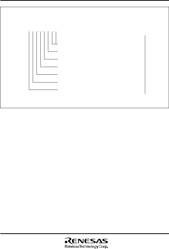
MITSUBISHI MICROCOMPUTERS
M37212M4/M8–XXXSP, M37212M6–XXXSP/FP
M37212EFSP/FP
SINGLE-CHIP 8-BIT CMOS MICROCOMPUTER for VOLTAGE SYNTHESIZER with ON-SCREEN DISPLAY CONTROLLER
Interrupt Input Polarity Register
b7 b6 b5 b4 b3 b2 b1 b0 |
|
|
|
|
|
|
|
|||||||
0 |
|
|
|
|
0 |
|
|
Interrupt input polarity register(RE) [Address 00F916] |
|
|
|
|||
|
|
|
|
|
|
|
|
|
|
|
|
|
|
|
|
|
|
|
|
|
|
|
B |
Name |
|
Functions |
After reset |
R |
W |
|
|
|
|
|
|
|
|
|
|
|
|
|
|
|
|
|
|
|
|
|
|
|
0, 1 |
Nothing is assigned. These bits are write disable bits. |
0 |
R |
— |
||
|
|
|
|
|
|
|
|
|
When these bits are read out, the values are “0.” |
|
|
|
||
|
|
|
|
|
|
|
|
|
|
|
|
|
|
|
|
|
|
|
|
|
|
|
2 |
Fix this bit to “0.” |
|
|
0 |
R |
W |
|
|
|
|
|
|
|
|
|
|
|
|
|
|
|
|
|
|
|
|
|
|
|
3 |
INT1 polarity switch bit |
0 |
: Positive polarity |
0 |
R |
W |
|
|
|
|
|
|
|
|
|
(RE3) |
1 |
: Negative polarity |
|
|
|
|
|
|
|
|
|
|
|
|
|
|
|
|
|
|
|
|
|
|
|
|
|
|
4 |
INT2 polarity switch bit |
0 |
: Positive polarity |
0 |
R |
W |
|
|
|
|
|
|
|
|
|
(RE4) |
1 |
: Negative polarity |
|
|
|
|
|
|
|
|
|
|
|
|
|
|
|
|
|
|
|
|
|
|
|
|
|
|
5 |
INT3 polarity switch bit |
0 |
: Positive polarity |
0 |
R |
W |
|
|
|
|
|
|
|
|
|
(RE5) |
1 |
: Negative polarity |
|
|
|
|
|
|
|
|
|
|
|
|
|
|
|
|
|
|
|
|
|
|
|
|
|
|
6 |
Nothing is assigned. This bit is a write disable bit. |
0 |
R |
— |
||
|
|
|
|
|
|
|
|
|
When this bit is read out, the value is “0.” |
|
|
|
||
|
|
|
|
|
|
|
|
|
|
|
|
|
|
|
|
|
|
|
|
|
|
|
7 |
Fix this bit to “0.” |
|
|
0 |
R |
W |
|
|
|
|
|
|
|
|
|
|
|
|
|
|
|
Fig. 8.3.6 Interrupt Input Polarity Register
Rev. 1.0
23

MITSUBISHI MICROCOMPUTERS
M37212M4/M8–XXXSP, M37212M6–XXXSP/FP M37212EFSP/FP
SINGLE-CHIP 8-BIT CMOS MICROCOMPUTER for VOLTAGE SYNTHESIZER with ON-SCREEN DISPLAY CONTROLLER
8.4 TIMERS
This microcomputer has 4 timers: timers 1 to 4. All timers are 8-bit timers with the 8-bit timer latch. The timer block diagram is shown in Figure 8.4.3.
All of the timers count down and their divide ratio is 1/(n+1), where n is the value of timer latch. By writing a count value to the corresponding timer latch (addresses 00F016 to 00F316 : timers 1 to 4), the value is also set to a timer, simultaneously.
The count value is decremented by 1. The timer interrupt request bit is set to “1” by a timer overflow at the next count pulse, after the count value reaches “0016.”
8.4.1 Timer 1
Timer 1 can select one of the following count sources:
•f(XIN)/16
•f(XIN)/4096
The count source of timer 1 is selected by setting bit 0 of timer 12 mode register 1 (address 00F416).
Timer interrupt request occurs at timer 1 overflow.
At reset, timers 3 and 4 are connected by hardware and “FF16” is automatically set in timer 3; “0716” in timer 4. The f(XIN)/16 is selected as the timer 3 count source. The internal reset is released by timer 4 overflow in this state and the internal clock is connected.
At execution of the STP instruction, timers 3 and 4 are connected by hardware and “FF16” is automatically set in timer 3; “0716” in timer 4. However, the f(XIN)/16 is not selected as the timer 3 count source.
So set both bit 0 of timer 34 mode register (address 00F516) and bit
6 at address 00C716 to “0” before execution of the STP instruction (f(XIN)/16 is selected as the timer 3 count source). The internal STP state is released by timer 4 overflow in this state and the internal clock is connected.
As a result of the above procedure, the program can start under a stable clock.
The timer-related registers is shown in Figures 8.4.1 and 8.4.2.
8.4.2 Timer 2
Timer 2 can select one of the following count sources:
•f(XIN)/16
•Timer 1 overflow signal
•External clock from the TIM2 pin
The count source of timer 2 is selected by setting bits 4 and 1 of timer 12 mode register (address 00F416). When timer 1 overflow signal is a count source for the timer 2, the timer 1 functions as an 8- bit prescaler.
Timer 2 interrupt request occurs at timer 2 overflow.
8.4.3 Timer 3
Timer 3 can select one of the following count sources:
•f(XIN)/16
•External clock from the HSYNC pin
•External clock from the TIM3 pin
The count source of timer 3 is selected by setting bits 5 and 0 of timer 34 mode register (address 00F516).
Timer 3 interrupt request occurs at timer 3 overflow.
8.4.4 Timer 4
Timer 4 can select one of the following count sources:
•f(XIN)/16
•f(XIN)/2
•Timer 3 overflow signal
The count source of timer 3 is selected by setting bits 1 and 4 of timer 34 mode register (address 00F516). When timer 3 overflow signal is a count source for the timer 4, the timer 3 functions as an 8- bit prescaler.
Timer 4 interrupt request occurs at timer 4 overflow.
Rev. 1.0
24
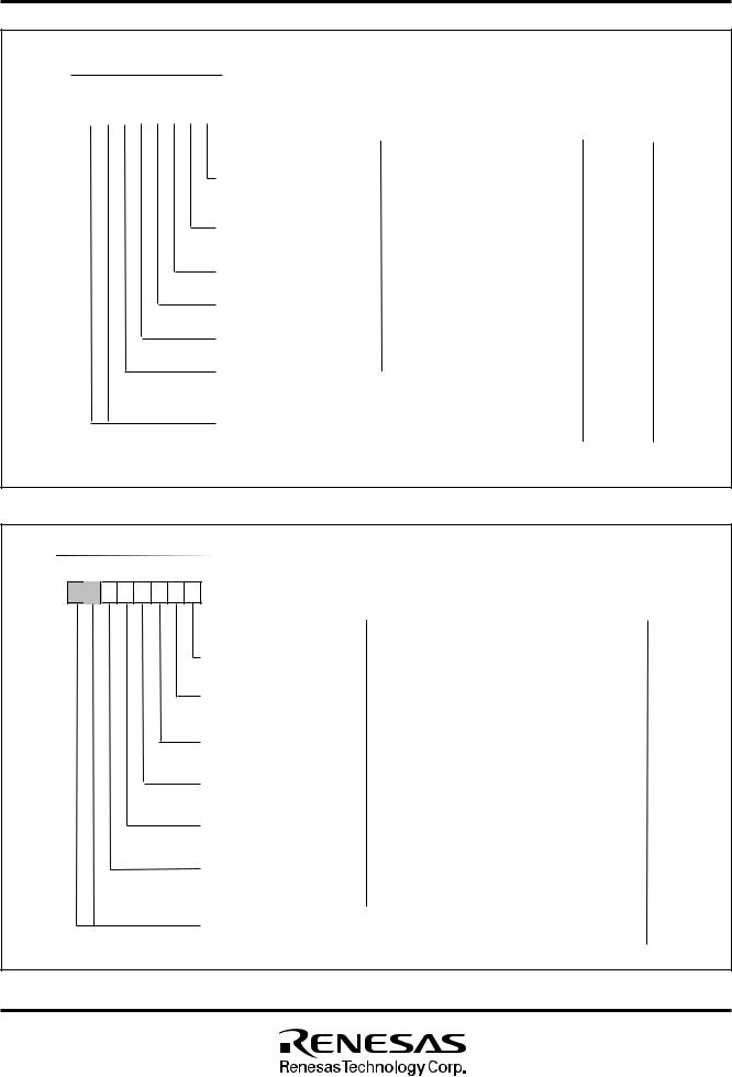
MITSUBISHI MICROCOMPUTERS
M37212M4/M8–XXXSP, M37212M6–XXXSP/FP
M37212EFSP/FP
SINGLE-CHIP 8-BIT CMOS MICROCOMPUTER for VOLTAGE SYNTHESIZER with ON-SCREEN DISPLAY CONTROLLER
Timer 12 Mode Register
b7b6 b5b4b3 b2b1b0 |
|
|
|
|
|
|
|||||||
|
|
0 |
|
|
|
|
|
Timer mode register (T12M) [Address 00F416] |
|
|
|
||
|
|
|
|
|
|
|
|
|
|
|
|
|
|
|
|
|
|
|
|
|
|
B |
Name |
Functions |
After reset |
R |
W |
|
|
|
|
|
|
|
|
|
|
|
|
|
|
|
|
|
|
|
|
|
|
0 |
Timer 1 count source |
0: f(XIN)/16 |
0 |
R |
W |
|
|
|
|
|
|
|
|
|
selection bit 1 (T12M0) |
1: f(XIN)/4096 |
|
|
|
|
|
|
|
|
|
|
|
|
|
|
|
|
|
|
|
|
|
|
|
|
|
1 |
Timer 2 count source |
0: Interrupt clock source |
0 |
R |
W |
|
|
|
|
|
|
|
|
|
selection bit (T12M1) |
1: External clock from TIM2 pin |
|
|
|
|
|
|
|
|
|
|
|
|
|
|
|
|
|
|
|
|
|
|
|
|
|
2 |
Timer 1 count |
0: Count start |
0 |
R |
W |
|
|
|
|
|
|
|
|
|
stop bit (T12M2) |
1: Count stop |
|
|
|
|
|
|
|
|
|
|
|
|
|
|
|
|
|
|
|
|
|
|
|
|
|
3 |
Timer 2 count stop bit |
0: Count start |
0 |
R |
W |
|
|
|
|
|
|
|
|
|
(T12M3) |
1: Count stop |
|
|
|
|
|
|
|
|
|
|
|
|
|
|
|
|
|
|
|
|
|
|
|
|
|
4 |
Timer 2 internal count |
0: f(XIN)/16 |
0 |
R |
W |
|
|
|
|
|
|
|
|
|
source selection bit 2 |
1: Timer 1 overflow |
|
|
|
|
|
|
|
|
|
|
|
|
(T12M4) |
|
|
|
|
|
|
|
|
|
|
|
|
|
|
|
|
|
|
|
|
|
|
|
|
|
|
5 |
Fix this bit to “0.” |
|
0 |
R |
W |
|
|
|
|
|
|
|
|
|
|
|
|
|
|
|
|
|
|
|
|
|
|
6, 7 |
Nothing is assigned. These bits are write disable bits. |
0 |
R |
— |
|
|
|
|
|
|
|
|
|
|
When these bits are read out, the values are “0.” |
|
|
|
|
Fig. 8.4.1 Timer 12 Mode Register
Timer 34 Mode Register
b7b6 b5b4b3 b2b1b0
Timer 34 mode register (T34M) [Address 00F516]
B |
Name |
|
Functions |
After reset |
R |
W |
0 |
Timer 3 count source |
0 |
: f(XIN)/16 |
0 |
R |
W |
|
selection bit (T34M0) |
1 |
: External clock source |
|
|
|
|
|
|
|
|
|
|
1 |
Timer 4 internal |
0 |
: Timer 3 overflow signal |
0 |
R |
W |
|
interrupt count source |
1 |
: f(XIN)/16 |
|
|
|
|
selection bit (T34M1) |
|
|
|
|
|
|
|
|
|
|
|
|
2 |
Timer 3 count stop bit |
0: Count start |
0 |
R |
W |
|
|
(T34M2) |
1: Count stop |
|
|
|
|
|
|
|
|
|
|
|
3 |
Timer 4 count stop bit |
0: Count start |
0 |
R |
W |
|
|
(T34M3) |
1: Count stop |
|
|
|
|
|
|
|
|
|
|
|
4 |
Timer 4 count source |
0: Internal clock source |
0 |
R |
W |
|
|
selection bit (T34M4) |
1: f(XIN)/2 |
|
|
|
|
|
|
|
|
|
|
|
5 |
Timer 3 external count |
0: TIM3 pin input |
0 |
R |
W |
|
|
source selection bit |
1: HSYNC pin input |
|
|
|
|
|
(T34M5) |
|
|
|
|
|
|
|
|
|
|
||
6, 7 |
Nothing is assigned. These bits are write disable bits. |
0 |
R |
— |
||
|
When these bits are read out, the values are “0.” |
|
|
|
||
|
|
|
|
|
|
|
Fig. 8.4.2 Timer 34 Mode Register
Rev. 1.0
25

MITSUBISHI MICROCOMPUTERS
M37212M4/M8–XXXSP, M37212M6–XXXSP/FP M37212EFSP/FP
SINGLE-CHIP 8-BIT CMOS MICROCOMPUTER for VOLTAGE SYNTHESIZER with ON-SCREEN DISPLAY CONTROLLER
Data bus
|
|
|
|
8 |
|
1/4096 |
|
|
Timer 1 latch (8) |
|
|
|
|
|
|
|
|
|
8 |
XIN |
1/2 |
1/8 |
|
Timer 1 (8) |
|
|
|
T12M0 |
|
|
|
|
T12M2 |
8 |
|
|
|
|
|
|
|
|
T12M4 |
|
|
|
|
|
8 |
|
|
|
|
Timer 2 latch (8) |
|
|
|
|
8 |
TIM2 |
|
|
|
Timer 2 (8) |
|
|
|
T12M1 |
|
|
|
|
T12M3 |
8 |
|
|
|
|
|
HSYNC |
|
|
|
8 |
|
|
|
|
FF16 |
TIM3 |
|
|
T34M5 |
Timer 3 latch (8) |
|
|
|
|
8 |
|
|
|
|
Timer 3 (8) |
|
|
|
T34M0 |
|
|
|
|
T34M2 |
8 |
|
|
|
|
|
Selection gate : |
|
|
|
8 |
Connected to black |
|
|
|
|
colored side at reset |
|
|
0716 |
|
|
|
|
T34M1 |
|
|
|
|
|
|
T12M : Timer 12 mode register |
|
|
Timer 4 latch (8) |
|
|
|
|
||
T34M : Timer 34 mode register |
|
|
8 |
|
|
|
|
T34M4 |
Timer 4 (8) |
|
|
|
|
|
|
|
|
T34M3 |
8 |
|
|
|
|
|
Timer 1 interrupt request
Timer 2 interrupt request
Reset
STP instruction
Timer 3 interrupt request
Timer 4 interrupt request
Notes 1: “H” pulse width of external clock inputs TIM2 and TIM3 needs 4 machine cycles or more.
2:When the external clock source is selected, timers 2 and 3 are counted at a rising edge of input signal.
3:In the stop mode or the wait mode, external clock inputs TIM2 and TIM3 cannot be used.
Fig. 8.4.3 Timer Block Diagram
Rev. 1.0
26

MITSUBISHI MICROCOMPUTERS
M37212M4/M8–XXXSP, M37212M6–XXXSP/FP M37212EFSP/FP
SINGLE-CHIP 8-BIT CMOS MICROCOMPUTER for VOLTAGE SYNTHESIZER with ON-SCREEN DISPLAY CONTROLLER
8.5 SERIAL I/O
This microcomputer has a built-in serial I/O which can either transmit or receive 8-bit data serially in the clock synchronous mode.
The serial I/O block diagram is shown in Figure 8.5.1. The synchronous clock I/O pin (SCLK), data output pin (SOUT), and data input pin
(SIN) also functions as port P4.
Bit 3 of the serial I/O mode register (address 00DC16) selects whether the synchronous clock is supplied internally or externally (from the
SCLK pin). When an internal clock is selected, bits 1 and 0 select whether f(XIN) or f(XCIN) is divided by 4, 16, 32, or 64. To use SIN pin for serial I/O, set the corresponding bit of the port P2 direction register (address 00C516) to “0.”
The operation of the serial I/O is described below. The operation of the serial I/O differs depending on the clock source; external clock or internal clock.
|
|
|
|
|
|
|
Data bus |
XIN |
1/2 |
1/2 |
|
Frequency |
|
|
|
|
divider |
|
|
||||
|
|
|
|
1/4 |
1/8 |
1/16 |
|
|
|
|
|
|
|
SM1 |
Selection gate : |
|
|
|
|
SM2 |
|
SM0 |
|
|
|
|
|
|
Connected to black |
||
|
|
Synchronization circuit |
|
|
|
|
|
|
|
|
|
|
|
colored side at reset. |
|
|
|
|
|
|
|
|
SM : Serial I/O mode register |
|
P41 latch |
|
|
|
|
|
|
SCLK |
|
|
|
Serial I/O counter (8) |
|
|
Serial I/O interrupt |
SM3 |
|
|
|
|
request |
||
|
|
|
|
|
|
||
|
|
|
|
|
|
|
|
|
P40 latch |
|
|
|
|
|
|
SOUT(/IN) |
|
SM5 : LSB |
MSB |
|
|
|
|
SM3 |
|
|
|
|
|
|
|
|
|
|
(See note) |
|
|||
SIN |
|
|
Serial I/O shift register (8) |
|
|
|
|
|
|
SM6 |
|
(Address 00DD16) |
|
||
|
|
|
|
|
8 |
|
|
Note : When the data is set in the serial I/O register (address 00DD 16), the register functions as the serial I/O shift register. |
|||||||
Fig. 8.5.1 Serial I/O Block Diagram
Rev. 1.0
27
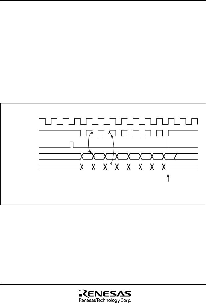
MITSUBISHI MICROCOMPUTERS
M37212M4/M8–XXXSP, M37212M6–XXXSP/FP M37212EFSP/FP
SINGLE-CHIP 8-BIT CMOS MICROCOMPUTER for VOLTAGE SYNTHESIZER with ON-SCREEN DISPLAY CONTROLLER
Internal clock : The serial I/O counter is set to “7” during the write cycle into the serial I/O register (address 00DD16), and the transfer clock goes HIGH forcibly. At each falling edge of the transfer clock after the write cycle, serial data is output from the SOUT pin. Transfer direction can be selected by bit 5 of the serial I/O mode register. At each rising edge of the transfer clock, data is input from the SIN pin and data in the serial I/O register is shifted 1 bit.
After the transfer clock has counted 8 times, the serial I/O counter becomes “0” and the transfer clock stops at HIGH. At this time the interrupt request bit is set to “1.”
External clock : The an external clock is selected as the clock source, the interrupt request is set to “1” after the transfer clock has been counted 8 counts. However, transfer operation does not stop, so the clock should be controlled externally. Use the external clock of 1 MHz or less with a duty cycle of 50%.
The serial I/O timing is shown in Figure 8.5.2. When using an external clock for transfer, the external clock must be held at HIGH for initializing the serial I/O counter. When switching between an internal clock and an external clock, do not switch during transfer. Also, be sure to initialize the serial I/O counter after switching.
Notes 1: On programming, note that the serial I/O counter is set by writing to the serial I/O register with the bit managing instructions, such as SEB and CLB.
2:When an external clock is used as the synchronous clock, write transmit data to the serial I/O register when the transfer clock input level is HIGH.
Synchronous clock
Transfer clock
Serial I/O register
write signal
(See note)
Serial I/O output
SOUT
D0 D1 D2 D3 D4 D5 D6 D7
Serial I/O input
SIN
Interrupt request bit is set to “1”
Note : When an internal clock is selected, the SOUT pin is at high-impedance after transfer is completed.
Fig. 8.5.2 Serial I/O Timing (for LSB first)
Rev. 1.0
28
MITSUBISHI MICROCOMPUTERS
M37212M4/M8–XXXSP, M37212M6–XXXSP/FP
M37212EFSP/FP
SINGLE-CHIP 8-BIT CMOS MICROCOMPUTER for VOLTAGE SYNTHESIZER with ON-SCREEN DISPLAY CONTROLLER
Serial I/O Mode Register
b7b6 b5b4b3 b2b1b0
|
|
|
0 |
|
|
|
|
Serial I/O mode register (SM) [Address 00DC16] |
|
|
|||
|
|
|
|
|
|
|
|
|
|
|
|
|
|
|
|
|
|
|
|
|
|
B |
Name |
|
Functions |
After reset R W |
|
|
|
|
|
|
|
|
|
0, 1 |
Internal synchronous |
b1 |
b0 |
0 |
R W |
|
|
|
|
|
|
|
|
|
clock selection bits |
0 |
0: f(XIN)/4 |
|
|
|
|
|
|
|
|
|
|
|
(SM0, SM1) |
0 |
1: f(XIN)/16 |
|
|
|
|
|
|
|
|
|
|
|
|
1 |
0: f(XIN)/32 |
|
|
|
|
|
|
|
|
|
|
|
|
1 |
1: f(XIN)/64 |
|
|
|
|
|
|
|
|
|
|
2 |
Synchronous clock |
0: External clock |
0 |
R W |
|
|
|
|
|
|
|
|
|
|
selection bit (SM2) |
1: Internal clock |
|
|
|
|
|
|
|
|
|
|
|
3 |
Serial I/O port |
0: P40, P41 |
0 |
R W |
|
|
|
|
|
|
|
|
|
|
selection bit (SM3) |
1: SOUT(/IN), SCLK |
|
|
|
|
|
|
|
|
|
|
|
4 |
Fix this bit to “0.” |
|
|
0 |
R W |
|
|
|
|
|
|
|
|
|
|
||||
|
|
|
|
|
|
|
|
5 |
Transfer direction |
0: LSB first |
0 |
R W |
|
|
|
|
|
|
|
|
|
|
selection bit (SM5) |
1: MSB first |
|
|
|
|
|
|
|
|
|
|
|
6 |
Serial input pin |
0: Input signal from SIN pin. |
0 |
R W |
|
|
|
|
|
|
|
|
|
|
selection bit (SM6) |
1: Input signal from SOUT pin. |
|
|
|
|
|
|
|
|
|
|
|
7 |
Nothing is assigned. This bit is a write disable bit. |
0 |
R — |
||
|
|
|
|
|
|
|
|
|
When this bit is read out, the value is “0.” |
|
|
||
|
|
|
|
|
|
|
|
|
|
|
|
|
|
Fig. 8.5.3 Serial I/O Mode Register
Rev. 1.0
29
 Loading...