


 Loading...
Mitsubishi M37211M2-XXXSP, M37210M4-XXXSP, M37210M3-XXXSP, M37210M3-XXXFP, M37210E4SP Datasheet
...MITSUBISHI MICROCOMPUTERS
M37210M3-XXXSP/FP, M37210M4-XXXSP, M37211M2-XXXSP M37210E4-XXXSP/FP, M37210E4SP/FP
SINGLE-CHIP 8-BIT CMOS MICROCOMPUTER for VOLTAGE SYNTHESIZER with ON-SCREEN DISPLAY CONTROLLER
DESCRIPTION
The M37210M3-XXXSP/FP is a single-chip microcomputer designed with CMOS silicon gate technology. It is housed in a 52-pin shrink plastic molded DIP or a 64-pin plastic molded QFP. This single-chip microcomputer is useful for the channel selection system for TVs because it provides PWM function, OSD display function and so on.
In addition to their simple instruction sets, the ROM, RAM, and I/O addresses are placed on the same memory map to enable easy programming.
The features of the M37210E4-XXXSP/FP and the M37210E4SP/FP are similar to those of the M37210M4-XXXSP except that these chips have a built-in PROM which can be written electrically.
The differences between the M37210M3-XXXSP/FP, the M37210 M4-XXXSP, and the M37211M2-XXXSP are the ROM size, the RAM size, and the PWM outputs as shown below. Accordingly, the following descriptions will be for the M37210M3-XXXSP/FP unless otherwise noted.
Type name |
ROM size |
RAM size |
6-bit PWM outputs |
M37210M3-XXXSP/FP |
12 K bytes |
256 bytes |
8 |
M37210M4-XXXSP |
16 K bytes |
320 bytes |
8 |
M37211M2-XXXSP |
8 K bytes |
192 bytes |
6 |
|
|
|
|
Note : After the reset, set the stack page selection bit which is set “1” to “0” because the internal RAM of the M37211M2-XXXSP is in only the zero page.
FEATURES |
|
|
• Number of basic instructions ..................................................... |
|
69 |
• Memory size ROM ................ |
12 K bytes (M37210M3-XXXSP/FP) |
|
|
16 K bytes (M37210M4-XXXSP) |
|
|
8 K bytes (M37211M2-XXXSP) |
|
RAM ................. |
256 bytes (M37210M3-XXXSP/FP) |
|
|
320 bytes (M37210M4-XXXSP) |
|
|
192 bytes (M37211M2-XXXSP) |
|
ROM for display......................................... |
3 K bytes |
|
RAM for display |
.......................................... |
72 bytes |
• The minimum instruction execution time |
|
|
........................................... 0.5μs (at 8MHz oscillation frequency) |
||
• Power source voltage ..................................................... |
|
5V ± 10% |
• Power dissipation .............................................................. |
|
110mW |
(at 4MHz oscillation frequency, VCC = 5.5V, at CRT display) |
||
• Subroutine nesting ............................................... |
96 levels (Max.) |
|
• Interrupts ....................................................... |
12 types, 12 vectors |
|
• 8-bit timers .................................................................................. |
|
4 |
• Programmable I/O ports |
|
|
(Ports P0, P1, P2, P3, P4) ......................................................... |
|
25 |
• Output ports (ports P5, P6) .......................................................... |
|
8 |
• Output ports (ports P52, P56) ..................................................... |
|
12 |
• 12 V withstand ports .................................................................... |
|
4 |
• Serial I/O ............................................................ |
8-bit 1 channel |
|
• PWM output circuit ............... |
(14-bit 1, 6-bit 8) ... |
M37210M3 |
|
|
M37210M4 |
|
(14-bit 1, 6-bit 6) .... |
M37211M2 |
PIN CONFIGURATION (TOP VIEW)
HSYNC → |
|
|
|
→ P52/R |
1 |
52 |
|||
VSYNC → |
|
|
|
→ P53/G |
2 |
51 |
|||
P60/PWM0 ← |
|
|
|
→ P54/B |
3 |
50 |
|||
P61/PWM1 ← |
|
|
|
→ P55/OUT |
4 |
49 |
|||
P62/PWM2 ← |
|
|
|
↔ P20 |
5 |
48 |
|||
P63/PWM3 ← |
|
|
|
↔ P21 |
6 |
47 |
|||
P00/PWM4 ↔ |
|
|
|
↔ P22 |
7 |
46 |
|||
P01/PWM5 ↔ |
|
|
|
↔ P23 |
8 |
45 |
|||
P02/PWM6 ↔ |
|
|
|
↔ P04 |
9 |
|
44 |
||
P03/PWM7 ↔ |
10 |
-M37211M2 |
-M37210M4 |
-M37210M3 |
43 |
↔ P05 |
|||
P42/SIN/A-D5 → |
|
|
|
|
|
↔ P06 |
|||
11 |
|
|
|
42 |
|||||
P41/SCLK ↔ |
|
|
|
|
|
↔ P07 |
|||
12 |
|
|
|
41 |
|||||
P40/SOUT (/IN) ↔ |
|
|
|
|
|
↔ P10 |
|||
13 |
|
|
|
40 |
|||||
|
→ |
|
XXXSP |
XXXSP |
XXXSP |
|
↔ P13 |
||
P34/INT1 |
16 |
37 |
|||||||
D-A |
← |
14 |
|
|
|
39 |
↔ P11 |
||
P35/INT2/A-D4 → |
15 |
|
|
|
38 |
↔ P12 |
|||
P33/TIM3 → |
|
|
|
|
|
↔ P14 |
|||
|
|
|
|
|
|||||
17 |
|
|
|
36 |
|||||
P32/TIM2 → |
|
|
|
|
|
← P15/A-D1 |
|||
18 |
|
|
|
35 |
|||||
|
↔ |
|
|
|
|
|
← P16/A-D2 |
||
P24 |
19 |
|
|
|
34 |
||||
|
↔ |
|
|
|
|
|
← P17/A-D3 |
||
P25 |
20 |
|
|
|
33 |
||||
|
↔ |
|
|
|
|
|
↔ P30 |
||
P26 |
21 |
|
|
|
32 |
||||
|
↔ |
|
|
|
|
|
↔ P31 |
||
P27 |
22 |
|
|
|
31 |
||||
CNVSS → |
|
|
|
|
|
← |
|
|
|
23 |
|
|
|
30 |
RESET |
||||
XIN → |
|
|
|
|
|
← OSC1 |
|||
24 |
|
|
|
29 |
|||||
XOUT ← |
|
|
|
|
|
→ OSC2 |
|||
25 |
|
|
|
28 |
|||||
|
|
|
|
|
|
|
|
VCC |
|
VSS |
|
26 |
|
|
|
27 |
|
||
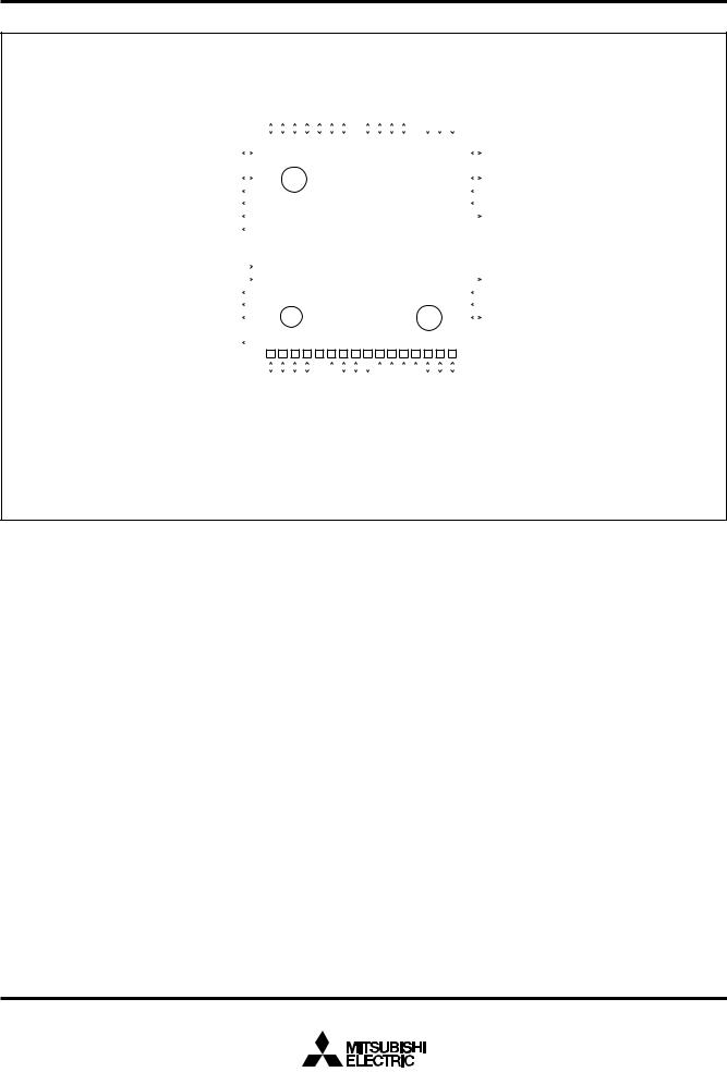
Outline 52P4B
Note : The M37211M2-XXXSP does not have the PWM6 and the PWM7.
• A-D comparator (5-bit resolution) ................................ |
5 channels |
• CRT display function |
|
Display characters ..................................... |
18 characters 2 lines |
|
(16 lines max.) |
Character kinds ................................................................ |
96 kinds |
Dot structure ............................................................. |
12 16 dots |
Character size .................................................................... |
3 kinds |
Character color kinds (It can be specified by the character) |
|
max. 7 kinds (R, G, B) |
|
Raster color (max. 7 kinds) |
|
Display layout |
|
Horizontal ..................................................................... |
64 levels |
Vertical ....................................................................... |
128 levels |
Bordering (horizontal and vertical) |
|
APPLICATION
TV
1
MITSUBISHI MICROCOMPUTERS
M37210M3-XXXSP/FP, M37210M4-XXXSP, M37211M2-XXXSP M37210E4-XXXSP/FP, M37210E4SP/FP
SINGLE-CHIP 8-BIT CMOS MICROCOMPUTER for VOLTAGE SYNTHESIZER with ON-SCREEN DISPLAY CONTROLLER
PIN CONFIGURATION (TOP VIEW)
|
|
|
|
P22 |
P23 |
P04 |
P05 |
P06 |
P07 |
P10 |
NC P11 |
P12 |
P13 |
P14 |
NC P15/A-D1 |
P16/A-D2 |
P17/A-D3 |
|
|
|
|
|
||||||||||||||||||||||||||||||||||
|
|
|
|
|
|
|
|
|
|
|
|
|
|
|
|
|
|
|
|
|
|
|
|
|
|
|
|
|
|
|
|
|
|
|
|
|
|
|
|
|
|
|
|
|
|
|
|
|
|
|
|
|
|
|
|
|
|
|
|
|
|
|
|
|
|
|
|
|
|
|
|
|
|
|
|
|
|
|
|
|
|
|
|
|
|
|
|
|
|
|
|
|
|
|
|
|
|
|
|
|
|
|
|
|
|
|
|
|
|
|
|
|
|
|
|
|
|
|
|
|
|
|
|
|
|
|
|
|
|
|
|
|
|
|
|
|
|
|
|
|
|
|
|
|
|
|
|
|
|
|
|
|
|
|
|
|
|
|
|
|
|
|
|
|
|
|
|
|
|
|
P21 |
|
|
|
48 |
|
47 |
|
46 |
|
45 |
|
44 |
|
43 |
|
42 |
|
41 |
|
40 |
|
39 |
|
38 |
|
37 |
|
36 |
|
35 |
|
34 |
|
33 |
|
|
|
|
P30 |
|||||||||||||||||
|
|
49 |
|
|
|
|
|
|
|
|
|
|
|
|
|
|
|
|
|
|
|
|
|
|
|
|
|
|
|
|
|
|
|
|
|
|
|
|
|
|
|
|
|
|
|
|
|
|
|
32 |
|
|
|
|||
|
|
|
|
|
|
|
|
|
|
|
|
|
|
|
|
|
|
|
|
|
|
|
|
|
|
|
|
|
|
|
|
|
|
|
|
|
|
|
|
|
|
|
|
|
|
|
|
|
||||||||
NC |
|
|
|
|
|
|
|
|
|
|
|
|
|
|
|
|
|
|
|
|
|
|
|
|
|
|
|
|
|
|
|
|
|
|
|
|
|
|
|
|
|
|
|
|
|
|
|
|
|
|
|
|
NC |
|||
50 |
|
|
|
|
|
|
|
|
|
|
|
|
|
|
|
|
|
|
|
|
|
|
|
|
|
|
|
|
|
|
|
|
|
|
|
|
|
|
|
|
|
|
|
|
|
|
|
31 |
||||||||
P20 |
|
|
|
|
|
|
|
|
|
|
|
|
|
|
|
|
|
|
|
|
|
|
|
|
|
|
|
|
|
|
|
|
|
|
|
|
|
|
|
|
|
|
|
|
|
|
|
|
|
|
|
|
|
|
P31 |
|
|
51 |
|
|
|
|
|
|
|
|
|
|
|
|
|
|
|
|
|
|
|
|
|
|
|
|
|
|
|
|
|
|
|
|
|
|
|
|
|
|
|
|
|
|
|
|
|
|
|
30 |
|
||||||
P55 /OUT |
|
|
|
|
|
|
|
|
|
|
|
|
|
|
|
|
|
|
|
|
|
|
|
|
|
|
|
|
|
|
|
|
|
|
|
|
|
|
|
|
|
|
|
|
|
|
|
|
|
|
|
|
|
|
|
|
|
|
|
|
|
|
|
|
|
|
|
|
|
|
|
|
|
|
|
|
|
|
|
|
|
|
|
|
|
|
|
|
|
|
|
|
|
|
|
|
|
|
|
|
|
|
|
|
|
|
|
|
|
|
RESET |
||
|
52 |
|
|
|
|
|
|
|
|
|
|
|
|
|
|
|
|
|
|
|
|
|
|
|
|
|
|
|
|
|
|
|
|
|
|
|
|
|
|
|
|
|
|
|
|
|
|
|
29 |
|
||||||
P54 /B |
|
|
|
|
|
|
|
|
|
|
|
|
|
|
|
|
|
|
|
|
|
|
|
|
|
|
|
|
|
|
|
|
|
|
|
|
|
|
|
|
|
|
|
|
|
|
|
|
|
|
|
|
|
|
OSC1 |
|
|
53 |
|
|
|
|
|
|
|
|
|
|
|
|
|
|
|
|
|
|
|
|
|
|
|
|
|
|
|
|
|
|
|
|
|
|
|
|
|
|
|
|
|
|
|
|
|
|
|
28 |
|
||||||
P53 /G |
|
|
|
|
|
|
|
|
|
|
|
|
|
|
|
|
|
|
|
|
|
|
|
|
|
|
|
|
|
|
|
|
|
|
|
|
|
|
|
|
|
|
|
|
|
|
|
|
|
|
|
|
|
|
OSC2 |
|
|
54 |
|
|
|
|
|
|
|
|
|
|
|
|
|
|
|
|
|
|
|
|
|
|
|
|
|
|
|
|
|
|
|
|
|
|
|
|
|
|
|
|
|
|
|
|
|
|
|
27 |
|
||||||
P52 /R |
|
|
|
|
|
|
|
|
|
|
|
|
|
|
|
|
|
|
|
|
|
|
|
|
|
|
|
|
|
|
|
|
|
|
|
|
|
|
|
|
|
|
|
|
|
|
|
|
|
|
|
|
|
|
Vcc |
|
|
55 |
|
|
|
|
|
|
|
|
|
|
|
|
|
|
|
|
|
|
|
|
|
|
|
|
|
|
|
|
|
|
|
|
|
|
|
|
|
|
|
|
|
|
|
|
|
|
|
26 |
|||||||
NC |
|
|
|
|
|
|
|
|
|
|
|
|
|
|
|
|
|
|
|
|
|
|
|
|
|
|
|
|
|
|
|
|
|
|
|
|
|
|
|
|
|
|
|
|
|
|
|
|
|
|
|
|
NC |
|||
56 |
|
|
|
|
|
|
|
|
|
|
|
M37210M3-XXXFP |
|
|
|
|
|
|
|
|
|
25 |
||||||||||||||||||||||||||||||||||
NC |
|
|
|
|
|
|
|
|
|
|
|
|
|
|
|
|
|
|
|
|
|
|
|
|
|
NC |
||||||||||||||||||||||||||||||
57 |
|
|
|
|
|
|
|
|
|
|
|
|
|
|
|
|
|
|
|
|
24 |
|
|
|
||||||||||||||||||||||||||||||||
|
|
|
|
|
|
|
|
|
|
|
|
|
|
|
|
|
|
|
|
|
|
|
|
|
|
|
|
|
|
|
|
|
|
|
|
|
|
|
|
|
|
|
|
|
|
|
|
|
||||||||
HSYNC |
|
|
|
|
|
|
|
|
|
|
|
|
|
|
|
|
|
|
|
|
|
|
|
|
|
|
|
|
|
|
|
|
|
|
|
|
|
|
|
|
|
|
|
|
|
|
|
|
|
|
|
|
|
|
VSS |
|
|
58 |
|
|
|
|
|
|
|
|
|
|
|
|
|
|
|
|
|
|
|
|
|
|
|
|
|
|
|
|
|
|
|
|
|
|
|
|
|
|
|
|
|
|
|
|
|
|
|
23 |
|||||||
VSYNC |
|
|
|
|
|
|
|
|
|
|
|
|
|
|
|
|
|
|
|
|
|
|
|
|
|
|
|
|
|
|
|
|
|
|
|
|
|
|
|
|
|
|
|
|
|
|
|
|
|
|
|
|
|
|
XOUT |
|
|
59 |
|
|
|
|
|
|
|
|
|
|
|
|
|
|
|
|
|
|
|
|
|
|
|
|
|
|
|
|
|
|
|
|
|
|
|
|
|
|
|
|
|
|
|
|
|
|
|
22 |
|
||||||
P60 /PWM0 |
|
|
|
|
|
|
|
|
|
|
|
|
|
|
|
|
|
|
|
|
|
|
|
|
|
|
|
|
|
|
|
|
|
|
|
|
|
|
|
|
|
|
|
|
|
|
|
|
|
|
|
|
|
|
XIN |
|
|
60 |
|
|
|
|
|
|
|
|
|
|
|
|
|
|
|
|
|
|
|
|
|
|
|
|
|
|
|
|
|
|
|
|
|
|
|
|
|
|
|
|
|
|
|
|
|
|
|
21 |
|
||||||
P61 /PWM1 |
|
|
|
|
|
|
|
|
|
|
|
|
|
|
|
|
|
|
|
|
|
|
|
|
|
|
|
|
|
|
|
|
|
|
|
|
|
|
|
|
|
|
|
|
|
|
|
|
|
|
|
|
|
|
CNVSS |
|
|
61 |
|
|
|
|
|
|
|
|
|
|
|
|
|
|
|
|
|
|
|
|
|
|
|
|
|
|
|
|
|
|
|
|
|
|
|
|
|
|
|
|
|
|
|
|
|
|
|
20 |
|
||||||
P62 /PWM2 |
|
|
|
|
|
|
|
|
|
|
|
|
|
|
|
|
|
|
|
|
|
|
|
|
|
|
|
|
|
|
|
|
|
|
|
|
|
|
|
|
|
|
|
|
|
|
|
|
|
|
|
|
|
|
P27 |
|
|
62 |
|
|
|
|
|
|
|
|
|
|
|
|
|
|
|
|
|
|
|
|
|
|
|
|
|
|
|
|
|
|
|
|
|
|
|
|
|
|
|
|
|
|
|
|
|
|
|
19 |
|
||||||
NC |
|
|
|
|
|
|
|
|
|
|
|
|
|
|
|
|
|
|
|
|
|
|
|
|
|
|
|
|
|
|
|
|
|
|
|
|
|
|
|
|
|
|
|
|
|
|
|
|
|
|
|
|
NC |
|||
63 |
|
|
|
|
|
|
|
|
|
|
|
|
|
|
|
|
|
|
|
|
|
|
|
|
|
|
|
|
|
|
|
|
|
|
|
|
|
|
|
|
|
|
|
|
|
|
|
18 |
||||||||
P63 /PWM3 |
|
|
|
|
|
|
|
|
|
|
|
|
|
|
|
|
|
|
|
|
|
|
|
|
|
|
|
|
|
|
|
|
|
|
|
|
|
|
|
|
|
|
|
|
|
|
|
|
|
|
|
|
|
|
NC |
|
|
64 |
|
|
|
|
|
|
|
|
|
|
|
|
|
|
|
|
|
|
|
|
|
|
|
|
|
|
|
|
|
|
|
|
|
|
|
|
|
|
|
|
|
|
|
|
|
|
|
17 |
|||||||
|
|
|
|
|
|
|
|
|
|
|
|
|
|
|
|
|
|
|
|
|
|
|
|
|
|
|
|
|
|
|
|
|
|
|
|
|
|
|
|
|
|
|
|
|
|
|
|
|
|
|
|
|
|
|
|
|
|
|
|
1 |
2 |
3 |
4 |
5 |
6 |
7 |
8 |
9 |
10 |
11 |
12 |
13 |
14 |
15 |
16 |
|
|
|
|
|
|
||||||||||||||||||||||||||||||||
|
|
|
|
|
|
|
|
|
|
|
|
|
|
|
|
|
|
|
|
|
|
|
|
|
|
|
|
|
|
|
|
|
|
|
|
|
|
|
||||||||||||||||||
|
|
|
|
|
|
|
|
|
|
|
|
|
|
|
|
|
|
|
|
|
|
|
|
|
|
|
|
|
|
|
|
|
|
|
|
|
|
|
|
|||||||||||||||||
|
|
|
|
P00/PWM4 |
P01/PWM5 |
P02/PWM6 |
P03/PWM7 |
NC |
P42/SIN/A-D5 |
P41/SCLK |
P40/SOUT/(/IN) |
D-A |
P35/INT2/A-D4 |
P34/INT1 |
P33/TIM3 |
P32/TIM2 |
P24 |
P25 |
P26 |
|
|
|
|
|
||||||||||||||||||||||||||||||||
Outline 64P6N-A
NC : No connection
2

FUNCTIONAL BLOCK DIAGRAM of M37210M3-XXXSP
Clock |
Clock |
|
(5V) |
(0V) (0V) |
||
input |
output |
Reset input |
||||
VCC |
VSS CNVSS |
|||||
XIN |
XOUT |
RESET |
||||
24 |
25 |
30 |
27 |
26 |
23 |
|
Clock |
|
Data bus |
|
|
|
|
generating |
|
|
|
|
||
circuit |
|
|
|
|
|
|
Timer count source selection circuit
RAM |
Program |
Program |
ROM |
Timer 1 |
|
T1 (8) |
|||||
256bytes |
counter |
counter |
12 K bytes |
||
(Note 2) |
PCH(8) |
PCL(8) |
(Note 3) |
|
|
Address bus |
|
|
|
Timer 2 |
|
|
|
|
T2 (8) |
TIM2
D-A HSYNCYSYNC OSC1 OSC2
14 |
1 |
2 |
29 |
28 |
 14-bit PWM circuit
6-bit PWM circuit
PWM7 |
PWM6 |
PWM5 |
PWM4 |
PWM3 |
PWM2 |
PWM1 |
PWM0 |
8-bit |
|
Processor |
Index |
Index |
Stack |
Timer 3 |
|
arithmetic |
Accumulator |
T3 (8) |
|||||
and logical |
status |
register X |
register Y |
pointer |
|||
A(8) |
|
||||||
unit |
register |
(8) |
(8) |
(8) |
TIM3 |
||
|
PS(8) |
|
|
|
|||
|
|
|
|
|
|
Timer 4
T4 (8)
|
|
|
|
|
|
|
|
|
|
|
|
A-D |
|
|
|
|
Interrupt interval |
|
|
||
|
|
|
|
|
|
|
|
|
|
|
|
compa- |
|
|
|
|
determination |
|
|
||
|
|
|
|
|
|
|
|
|
|
|
|
rator |
|
|
|
|
circuit |
|
|
||
|
P0(8) |
|
|
|
|
|
|
P1(8) |
|
P2(8) |
|
|
INT1 |
|
|
INT1, INT2 |
P4(3) |
||||
|
|
|
|
|
|
|
|
|
|
INT2 |
P3(6) |
|
|||||||||
|
|
|
|
|
|
|
|
|
|
|
|
|
|
|
|
|
|
|
|
||
|
|
|
|
|
|
|
|
|
|
|
|
|
|
5 |
|
|
|
|
|
|
|
|
|
|
|
|
|
A-D1 |
A-D2 |
A-D3 |
|
|
3 |
|
|
|
|
|
|
|
|
|
|
|
|
|
|
|
|
|
|
|
|
|
A-D4 |
|
|
|
A-D5 |
|
|
||||
41 |
42 43 44 |
10 |
9 |
8 |
7 |
33 34 35 |
36 37 38 39 |
40 |
22 21 20 19 45 |
46 47 |
48 |
15 16 17 |
18 31 |
32 |
11 12 |
13 |
|||||
|
|
||||||||||||||||||||
|
I/O port P0 |
|
|
|
|
I/O port P1 |
|
I/O port P2 |
|
|
I/O port P3 |
|
|
I/O port P4 |
|||||||
Notes 1 : The M37211M2-XXXSP does not have PWM outputs of pins 9 and 10. 2 : 320 bytes for M37210M4-XXXSP and 192 bytes for M37211M2-XXXSP 3 : 16 K bytes for M37210M4-XXXSP and 8 K bytes for M37211M2-XXXSP
3
|
|
Control signal |
|
|
|
|
|||
|
|
Instruction decoder |
|
|
|
|
|||
|
|
Instruction |
CRT circuit |
||||||
|
|
|
register |
|
|
|
|
|
|
SI/O(8) |
|
|
|
|
|
|
|
||
SIN |
SCLK |
SOUT |
P6(4) |
|
|
P5(4) |
|
||
|
|
|
|
|
|
||||
|
|
|
|
|
|
OUT |
B |
G |
R |
|
|
6 |
5 |
4 |
3 |
49 50 51 52 |
|||
|
|
Output port P6 |
Video signal output |
||||||
DISPLAY SCREEN-ON with |
VOLTAGE for MICROCOMPUTER CMOS BIT-8 CHIP-SINGLE |
CONTROLLER |
SYNTHESIZER |
XXXSP-M37211M2 XXXSP,-M37210M4 XXXSP/FP,-M37210M3 M37210E4SP/FP XXXSP/FP,-M37210E4 |
MICROCOMPUTERS MITSUBISHI |

MITSUBISHI MICROCOMPUTERS
M37210M3-XXXSP/FP, M37210M4-XXXSP, M37211M2-XXXSP M37210E4-XXXSP/FP, M37210E4SP/FP
|
SINGLE-CHIP 8-BIT CMOS MICROCOMPUTER for VOLTAGE SYNTHESIZER |
|||
|
|
|
|
with ON-SCREEN DISPLAY CONTROLLER |
|
|
|
|
|
FUNCTIONS |
|
|
|
|
|
|
|
|
|
|
Parameter |
|
Functions |
|
Number of basic instructions |
|
|
|
69 |
Instruction execution time |
|
|
|
0.5μs (the minimum instruction execution time, at 8MHz oscillation frequency) |
Clock frequency |
|
|
|
8MHz |
|
M37210M3-XXXSP/FP |
|
ROM |
12 K bytes |
|
|
RAM |
256 bytes |
|
|
|
|
||
Memory size |
M37210M4-XXXSP |
|
ROM |
16 K bytes |
|
RAM |
320 bytes |
||
|
|
|
||
|
M37211M2-XXXSP |
|
ROM |
8 K bytes |
|
|
RAM |
192 bytes |
|
|
|
|
||
|
P0 |
|
I/O |
8-bit 1 (can be used as N-channel open-drain output and PWM4-PWM7)(Note) |
|
P10 – P14 |
|
I/O |
5-bit 1 (CMOS 3-state output) |
|
P15 – P17 |
|
Input |
3-bit 1 (can be used as A-D input) |
|
P2 |
|
I/O |
8-bit 1 (CMOS 3-state output) |
Input/Output ports |
P30, P31 |
|
I/O |
2-bit 1 (CMOS 3-state input/output) |
P32, P35 |
|
Input |
4-bit 1 (can be used as timer input pins, INT input pins and A-D input pins) |
|
|
|
|||
|
P40, P41 |
|
I/O |
2-bit 1 (can be used as N-channel open-drain output and serial I/O function pins) |
|
P42 |
|
Input |
1-bit 1 (can be used as serial I/O and A-D input) |
|
P5 |
|
Output |
4-bit 1 (can be used as R, G, B, OUT pins) |
|
P6 |
|
Output |
4-bit 1 (can be used as N-channel open-drain output and PWM0-PWM3 output pins) |
Serial I/O |
|
|
|
8-bit 1 |
Timers |
|
|
|
8-bit timer 4 |
Subroutine nesting |
|
|
|
96 levels (max.) |
|
|
|
|
Two external interrupts, four internal timer interrupts, |
Interrupt |
|
|
|
one serial I/O interrupt, one CRT interrupt, one f(XIN)/4096 |
|
|
|
|
interrupt, one VSYNC interrupt, BRK instruction |
|
|
|
|
|
Clock generating circuit |
|
|
|
Built-in circuit (externally connected a ceramic resonator or a quartz-crystal oscillator) |
Power source voltage |
|
|
|
5V ± 10% |
|
at CRT display ON |
|
110mW (at 4MHz oscillation frequency, VCC = 5.5V, Typ.) |
|
Power dissipation |
at CRT display OFF |
|
55mW (at 4MHz oscillation frequency, VCC = 5.5V, Typ.) |
|
|
at stop mode |
|
1.65mW (Max.) |
|
Operating temperature range |
|
|
|
−10 to 70°C |
Device structure |
|
|
|
CMOS silicon gate process |
Package |
M37210M3-XXXSP, M37210M4-XXXSP, M37211M2-XXXSP |
52-pin shrink plastic molded DIP |
||
M37210M3-XXXFP |
|
64-pin plastic molded QFP |
||
|
|
|||
|
Number of character |
|
18 characters 2 lines : maximum 16 lines (by software) |
|
|
Character dot construction |
|
12 16 dots |
|
CRT display function |
Kinds of characters |
|
96 kinds |
|
Character size |
|
3 kinds |
||
|
|
|||
|
Kinds of color |
|
7 kinds max, (R, G, B) : can be specified by character unit |
|
|
Display position (horizontal, vertical) |
64 levels (horizontal) 128 levels (vertical) |
||
|
|
|
|
|
Note : The M37211M2-XXXSP can be also used as PWM4 and PWM5.
4

MITSUBISHI MICROCOMPUTERS
M37210M3-XXXSP/FP, M37210M4-XXXSP, M37211M2-XXXSP M37210E4-XXXSP/FP, M37210E4SP/FP
|
|
|
|
|
SINGLE-CHIP 8-BIT CMOS MICROCOMPUTER for VOLTAGE SYNTHESIZER |
|
|
|
|
|
with ON-SCREEN DISPLAY CONTROLLER |
|
|
|
|
|
|
PIN DESCRIPTION |
|
|
|||
|
|
|
|
|
|
|
Pin |
Name |
Input / |
Functions |
|
|
Output |
||||
|
|
|
|
|
|
|
|
|
|
|
|
|
VCC, |
Power source voltage |
|
Apply voltage of 5V ± 10% to VCC, and 0V to VSS. |
|
|
VSS |
|
|
|
|
|
|
|
|
|
|
|
CNVSS |
CNVSS |
|
This is connected to VSS. |
|
|
|
|
Reset input |
Input |
To enter the reset state, the reset input pin must be kept at a “L” for 2μs or more (under nor- |
|
RESET |
||||
|
|
|
|
|
mal VCC conditions). |
|
|
|
|
|
If more time is needed for the crystal oscillator to stabilize, this “L” condition should be main- |
|
|
|
|
|
tained for the required time. |
|
|
|
|
|
|
|
XIN |
Clock input |
Input |
This chip has an internal clock generating circuit. To control generating frequency, an exter- |
|
|
|
|
|
|
nal ceramic resonator or a quartz-crystal oscillator is connected between the XIN and |
|
XOUT |
Clock output |
Output |
XOUT pins. If an external clock is used, the clock source should be connected the XIN pin and |
|
|
|
|
|
|
the XOUT pin should be left open. |
|
φ |
Timing output |
Output |
This is the timing output pin. |
|
|
P00 – P07 |
I/O port P0 |
I/O |
Port P0 is an 8-bit I/O port with directional registers allowing each I/O bit to be individually |
|
|
|
|
|
|
programmed as input or output. At reset, this port is set to input mode. The output structure |
|
|
|
|
|
is CMOS output. |
|
|
|
|
|
The output structure is N-channel open-drain output. When PWM4, PWM5, PWM6 and |
|
|
|
|
|
PWM7 are used, P00, P01, P02 and P03 are in common with PWM output pins of PWM4, |
|
|
|
|
|
PWM5, PWM6 and PWM7. |
|
|
|
|
|
|
|
P11 – P14 |
I/O port P1 |
I/O |
Ports P10, P11, P12, P13 and P14 are 5-bit I/O ports and have basically the same functions |
|
|
|
|
|
|
as port P0. The output structure is CMOS output. |
|
|
|
|
|
|
|
P15 – P17 |
Input port P1 |
Input |
Ports P15, P16 and P17 are 3-bit input ports and they are in common with input pins of A-D |
|
|
|
|
|
|
comparator (A-D1, A-D2 and A-D3). |
|
|
|
|
|
|
|
P20 – P27 |
I/O port P2 |
I/O |
Port P2 is an 8-bit I/O port and has basically the same functions as port P0. |
|
|
|
|
|
|
The output structure is CMOS output. |
|
|
|
|
|
|
|
P30, P31 |
I/O port P3 |
I/O |
Ports P30 and P31 are 2-bit I/O ports and have basically the same functions as port P0. |
|
|
|
|
|
|
The output structure is CMOS output. |
|
|
|
|
|
|
|
P32 – P35 |
Input port P3 |
Input |
Ports P32, P33, P34 and P35 are 4-bit input ports and ports P32 and P33 are in common |
|
|
|
|
|
|
with external clock input pins of timers 2 and 3. Ports P34 and P35 are in common with |
|
|
|
|
|
external interrupt input pins INT1 and INT2. Port P35 is in common with an input pin of A-D |
|
|
|
|
|
comparator (A-D4). |
|
|
|
|
|
|
|
P40, P41 |
I/O port P4 |
I/O |
Ports P40 and P41 are 2-bit I/O ports and have basically the same functions as port P0. |
|
|
|
|
|
|
When serial I/O is used, ports P40 and P41 are in common with SOUT pin and SCLK pin, re- |
|
|
|
|
|
spectively. |
|
|
|
|
|
|
|
P42 |
Input port P4 |
Input |
Port P42 is an 1-bit Input port, and it is common with an input pin of A-D comparator (A-D5) |
|
|
|
|
|
|
and serial input pin (SIN). |
|
|
|
|
|
|
|
P60 – P63 |
Output port P6 |
Output |
Port P6 is an 4-bit output port. The output structure is N-channel open-drain. This port is in |
|
|
|
|
|
|
common with 6-bit PWM output pins PWM0-PWM3. |
|
|
|
|
|
|
|
OSC1, |
Clock input for CRT |
Input |
This is the I/O pins of the clock generating circuit for the CRT display function. |
|
|
OSC2 |
display |
Output |
|
|
|
|
|
Clock output for CRT |
|
|
|
|
|
display |
|
|
|
HSYNC |
HSYNC input |
Input |
This is the horizontal synchronizing signal input for CRT display. |
|
|
|
|
|
|
|
|
VSYNC |
VSYNC input |
Input |
This is the vertical synchronizing signal input for CRT display. |
|
|
|
|
|
|
|
|
R, G, B, |
CRT output |
Output |
This is a 4-bit output pin for CRT display. The output structure is CMOS output. This is in |
|
|
OUT |
|
|
common with port P52 – P55. |
|
|
D-A |
DA Output |
Output |
This is an output pin for 14-bit PWM. |
|
|
|
|
|
|
|
5

MITSUBISHI MICROCOMPUTERS
M37210M3-XXXSP/FP, M37210M4-XXXSP, M37211M2-XXXSP M37210E4-XXXSP/FP, M37210E4SP/FP
SINGLE-CHIP 8-BIT CMOS MICROCOMPUTER for VOLTAGE SYNTHESIZER with ON-SCREEN DISPLAY CONTROLLER
FUNCTIONAL DESCRIPTION
Central Processing Unit (CPU)
The M37210M3-XXXSP/FP uses the standard 740 family instruction set. Refer to the table of 740 family addressing modes and machine instructions or the SERIES 740 áSoftwareñ User’s Manual for details on the instruction set.
Machine-resident 740 family instructions are as follows :
The FST and SLW instruction cannot be used.
The MUL, DIV, WIT, and STP instruction can be used.
CPU Mode Register
The CPU mode register is allocated at address 00FB16. The CPU mode register contains the stack page selection bit.
7 |
|
|
|
|
|
|
|
|
0 |
|
|
|
|
|
||||||
1 |
1 |
1 |
1 |
1 |
|
|
0 |
0 |
CPU mode register |
|||||||||||
|
|
|
|
|
|
|
|
|
|
|
|
|
|
|
|
(CPUM : address 00FB16) |
||||
|
|
|
|
|
|
|
|
|
|
|
|
|
|
|
|
|
|
|
Fix these bits to “002” |
|
|
|
|
|
|
|
|
|
|
|
|
|
|
|
|
|
|
||||
|
|
|
|
|
|
|
|
|
|
|
|
|
|
|
|
|
|
|
Stack page selection bit (Note) |
|
|
|
|
|
|
|
|
|
|
|
|
|
|
|
|
|
|
|
|||
|
|
|
|
|
|
|
|
|
|
|
|
|
|
|
|
0 |
: Zero page |
|||
|
|
|
|
|
|
|
|
|
|
|
|
|
|
|
|
1 |
: 1 page |
|||
|
|
|
|
|
|
|
|
|
|
|
|
|
|
|
|
|
|
|
Fix these bits to “11112” |
|
|
|
|
|
|
|
|
|
|
|
|
|
|
|
|
|
|
|
|
||
Note : Please beware of this bit when programming because it is set to “1” after the reset release.
Especially the internal RAM of the M37211M2-XXXSP is in the zero page, so be sure to set this bit to “0”.
Fig. 1 Structure of CPU mode register
6

MITSUBISHI MICROCOMPUTERS
M37210M3-XXXSP/FP, M37210M4-XXXSP, M37211M2-XXXSP M37210E4-XXXSP/FP, M37210E4SP/FP
SINGLE-CHIP 8-BIT CMOS MICROCOMPUTER for VOLTAGE SYNTHESIZER with ON-SCREEN DISPLAY CONTROLLER
MEMORY
Special Function Register (SFR) Area
The special function register (SFR) area in the zero page contains control registers such as I/O ports and timers.
RAM
RAM is used for data storage and for stack area of subroutine calls and interrupts.
ROM
ROM is used for sroring user programs as well as the interrupt vector area.
RAM for Display
RAM for display is used for specifing the character codes and colors to display.
Interrupt Vector Area
The interrupt vector area contains reset and interrupt vectors.
Zero Page
The 256 bytes from addresses 000016 to 00FF16 are called the zero page area. The internal RAM and the special function registers
(SFR) are allocated to this area.
The zero page addressing mode can be used to specify memory and register addresses in the zero page area. Access to this area with only 2 bytes is possible in the zero page addressing mode.
Special Page
The 256 bytes from addresses FF0016 to FFFF16 are called the special page area. The special page addressing mode can be used to specify memory addresses in the special page area. Access to this area with only 2 bytes is possible in the special page addressing mode.
ROM for Display
ROM for display is used for storing character data.
|
ü |
|
ü |
|
ü |
000016 |
|
|
ï |
|
ï |
||
|
ï |
|
RAM |
|
||
|
ï |
|
ï |
(192 bytes) |
ï |
|
|
ý |
|
ý |
ý |
|
|
|
|
for |
|
|||
|
ï |
|
ï |
ï |
|
|
|
RAM |
M37211M2 |
|
|||
RAM |
ï |
ï |
ï |
00BF16 |
||
þ |
(256 bytes) |
þ |
|
þ |
||
(320 bytes) |
|
|
||||
|
for |
|
|
|
|
|
for |
|
|
|
|
|
|
|
M37210M3 |
|
|
|
|
|
M37210M4 |
ü |
ü |
|
|
|
|
|
|
|
00FF16 |
|||
|
|
|
|
|||
|
ï |
|
ï |
|
|
|
|
|
ï |
|
|
|
|
|
ï |
|
ý |
|
|
|
|
ý |
|
ï |
|
|
|
|
ï |
|
ï |
|
|
|
|
|
þ |
|
|
013F16 |
|
|
ï |
|
|
|
|
|
|
|
|
|
|
|
|
|
þ |
|
|
|
|
017F16 |
|
|
|
|
|
ü |
200016 |
|
|
|
|
|
ï |
|
|
|
|
|
|
|
|
|
|
|
|
|
ï |
|
|
|
RAM for display (Note)ý |
|
|||
|
|
|
|
(72 bytes)ï |
|
|
|
|
|
|
|
ï |
20B116 |
|
|
|
|
|
þ |
|
|
|
|
|
|
ü |
300016 |
|
|
|
|
|
ï |
35FF16 |
|
|
|
|
|
ï |
|
|
|
|
|
|
|
|
|
|
ROM for displayý |
|
|||
|
|
|
|
(3 K bytes)ï |
380016 |
|
|
|
|
|
|
ï |
3DFF16 |
|
|
|
|
|
þ |
|
|
|
|
|
|
|
|
|
ü |
|
|
|
|
C00016 |
|
|
|
|
|
|
|
|
ï |
|
|
|
|
D00016 |
|
ï |
|
ü |
|
|
|
|
ï |
|
|
|
|
|
|
ï |
|
ï |
|
ü |
|
|
ï |
|
ï |
|
E00016 |
|
|
ï |
|
ï |
|
ï |
|
|
|
|
|
|||
|
ï |
|
ï |
|
ï |
|
ROM |
ï |
|
ï |
|
ï |
|
ï |
|
ï |
|
ï |
|
|
(16 K bytes) |
ï |
|
|
|
||
ROM |
ï |
|
ï |
|
||
|
ý |
|
|
|||
for |
(12 K bytes) ï |
ROM |
ï |
|
||
ï |
|
|||||
M37210M4 |
for |
ý |
(8 K bytes) |
ï |
|
|
ï |
FF0016 |
|||||
|
ï |
M37210M3 |
ï |
for |
ý |
|
|
ï |
ï |
|
|||
|
ï |
|
M37211M2 |
|
||
|
|
ï |
ï |
|
||
|
ï |
|
|
|
||
|
|
ï |
|
ï |
|
|
|
ï |
|
|
|
||
|
ï |
|
ï |
|
ï |
|
|
ï |
|
ï |
|
ï |
|
|
ï |
|
ï |
|
ï FFDE16 |
|
|
ï |
|
ï |
|
ï |
FFFF16 |
|
þ |
|
þ |
|
þ |
|
|
|
|
|
|||
Fig. 2 Memory map
ü
ï
ï
ï
ýï Zero page
ï
SFR area ï
þ
Not used
Not used
Not used
Not used
ü
ï
ï
ï
ýSpecial page
ï
ï
Interrupt vector area ï
þ
Note : Refer to Table 6. Contents of CRT display RAM
7

MITSUBISHI MICROCOMPUTERS
M37210M3-XXXSP/FP, M37210M4-XXXSP, M37211M2-XXXSP M37210E4-XXXSP/FP, M37210E4SP/FP
SINGLE-CHIP 8-BIT CMOS MICROCOMPUTER for VOLTAGE SYNTHESIZER with ON-SCREEN DISPLAY CONTROLLER
00C016 |
Port P0 |
00E016 |
Horizontal position register |
00C116 |
Port P0 directional register |
00E116 |
Vertical position register 1 (block 1) |
00C216 |
Port P1 |
00E216 |
Vertical position register 2 (block 2) |
00C316 |
Port P1 directional register |
00E316 |
|
00C416 |
Port P2 |
00E416 |
Character size register |
00C516 |
Port P2 directional register |
00E516 |
Border selection register |
00C616 |
Port P3 |
00E616 |
Color register 0 |
00C716 |
Port P3 directional register |
00E716 |
Color register 1 |
00C816 |
Port P4 |
00E816 |
Color register 2 |
00C916 |
Port P4 directional register |
00E916 |
Color register 3 |
00CA16 |
Port P5 |
00EA16 |
CRT control register |
00CB16 |
Port P5 control register |
00EB16 |
|
00CC16 |
Port P6 |
00EC16 |
CRT port control register |
00CD16 |
Port P6 directional register |
00ED16 |
|
00CE16 |
14DA-H register |
00EE16 |
A-D mode register |
00CF16 |
14DA-L register |
00EF16 |
A-D control register |
00D016 |
PWM0 register |
00F016 |
Timer 1 |
00D116 |
PWM1 register |
00F116 |
Timer 2 |
00D216 |
PWM2 register |
00F216 |
Timer 3 |
00D316 |
PWM3 register |
00F316 |
Timer 4 |
00D416 |
PWM4 register |
00F416 |
Timer 12 mode register |
00D516 |
PWM output control register 1 |
00F516 |
Timer 34 mode register |
00D616 |
PWM output control register 2 |
00F616 |
PWM5 register |
00D716 |
Interrupt Interval determination register |
00F716 |
PWM6 register (Note) |
00D816 |
Interrupt Interval determination control register |
00F816 |
PWM7 register (Note) |
00D916 |
|
00F916 |
|
00DA16 |
|
00FA16 |
|
00DB16 |
|
00FB16 |
CPU mode register |
00DC16 |
Serial I/O mode register |
00FC16 |
Interrupt request register 1 |
00DD16 |
Serial I/O register |
00FD16 |
Interrupt request register 2 |
00DE16 |
|
00FE16 |
Interrupt control register1 |
00DF16 |
|
00FF16 |
Interrupt control register2 |
Note : The M37211M2-XXXSP dose not have this register
Fig. 3 Memory map of special function register (SFR )
8

MITSUBISHI MICROCOMPUTERS
M37210M3-XXXSP/FP, M37210M4-XXXSP, M37211M2-XXXSP M37210E4-XXXSP/FP, M37210E4SP/FP
SINGLE-CHIP 8-BIT CMOS MICROCOMPUTER for VOLTAGE SYNTHESIZER with ON-SCREEN DISPLAY CONTROLLER
INTERRUPTS
Interrupts can be caused by 12 different sources consisting of 3 external, 7 internal, 1 software, and reset.
Interrupts are vectored interrupts with priorities shown in Table 1. Reset is also included in the table because its operation is similar to an interrupt.
When an interrupt is accepted, the registers are pushed, interrupt disable flag I is set, and the program jumps to the address specified in the vector table. The interrupt request bit is cleared automatically. The reset can never be disabled. Other interrupts are disabled when the interrupt disable flag is set.
Table 1. Interrupt vector addresses and priority
All interrupts except the BRK instruction interrupt have an interrupt request bit and an interrupt enable bit. The interrupt request bits are in interrupt request registers 1 and 2 and the interrupt enable bits are in interrupt control registers 1 and 2. Figure 4 shows the structure of the interrupt request registers 1 and 2 and interrupt control registers
1 and 2.
Interrupts other than the BRK instruction interrupt and reset are accepted when the interrupt enable bit is “1”, interrupt request bit is “1”, and the interrupt disable flag is “0”. The interrupt request bit can be reset with a program, but not set. The interrupt enable bit can be set and reset with a program.
Reset is treated as a non-maskable interrupt with the highest priority. Figure 5 shows interrupts control.
Interrupt sources |
Priority |
Vector addresses |
Remarks |
|
|
|
|
|
|
Reset |
1 |
FFFF16, |
FFFE16 |
Non-maskable |
|
|
|
|
|
CRT interrupt |
2 |
FFFD16, |
FFFC16 |
|
|
|
|
|
|
INT2 interrupt |
3 |
FFFB16, |
FFFA16 |
Active edge selectable |
|
|
|
|
|
INT1 interrupt |
4 |
FFF916, |
FFF816 |
Active edge selectable |
|
|
|
|
|
Timer 4 interrupt |
5 |
FFF516, |
FFF416 |
|
|
|
|
|
|
f(XIN)/4096 interrupt |
6 |
FFF316, |
FFF216 |
|
|
|
|
|
|
VSYNC interrupt |
7 |
FFF116, |
FFF016 |
Active edge selectable |
|
|
|
|
|
Timer 3 interrupt |
8 |
FFEF16, |
FFEE16 |
|
|
|
|
|
|
Timer 2 interrupt |
9 |
FFED16, |
FFEC16 |
|
|
|
|
|
|
Timer 1 interrupt |
10 |
FFEB16, |
FFEA16 |
|
|
|
|
|
|
Serial I/O interrupt |
11 |
FFE916, |
FFE816 |
|
|
|
|
|
|
BRK instruction interrupt |
12 |
FFDF16, |
FFDE16 |
Non-maskable software interrupt |
|
|
|
|
|
9

MITSUBISHI MICROCOMPUTERS
M37210M3-XXXSP/FP, M37210M4-XXXSP, M37211M2-XXXSP M37210E4-XXXSP/FP, M37210E4SP/FP
SINGLE-CHIP 8-BIT CMOS MICROCOMPUTER for VOLTAGE SYNTHESIZER with ON-SCREEN DISPLAY CONTROLLER
7 |
0 |
7 |
0 |
||||||||||||||
0 |
0 |
|
|
|
|
|
|
|
|
|
|
|
|
||
|
|
|
|
|
|
|
|
|
|
|
|
|
|
|
|
|
|
|
|
|
|
|
|
|
|
|
|
|
|
|
|
|
|
|
|
|
|
|
|
|
|
|
|
|
|
|
|
|
|
|
|
|
|
|
|
|
|
|
|
|
|
|
|
|
|
|
|
|
|
|
|
|
|
|
|
|
|
|
|
|
|
|
|
|
|
|
|
|
|
|
|
|
|
|
|
|
|
|
|
|
|
|
|
|
|
|
|
|
|
|
|
|
7 |
|
|
|
0 |
|
|
|
||||||||||
Interrupt request register 1 |
0 |
|
|
|
|
|
|
|
|
|
|
|
|
|
Interrupt request register 2 |
|||
(IREQ1 : address 00FC16) |
|
|
|
|
|
|
|
|
|
|
|
|
|
|
|
|
|
(IREQ2 : address 00FD16) |
Timer 1 interrupt request bit |
|
|
|
|
|
|
|
|
|
|
|
|
|
|
|
|
|
INT1 interrupt request bit |
|
|
|
|
|
|
|
|
|
|
|
|
|
|
|
|
|||
Timer 2 interrupt request bit |
|
|
|
|
|
|
|
|
|
|
|
|
|
|
|
|
|
INT2 interrupt request bit |
|
|
|
|
|
|
|
|
|
|
|
|
|
|
|
|
|||
Timer 3 interrupt request bit |
|
|
|
|
|
|
|
|
|
|
|
|
|
|
|
|
|
Serial I/O1 interrupt request bit |
|
|
|
|
|
|
|
|
|
|
|
|
|
|
|
|
|||
Timer 4 interrupt request bit |
|
|
|
|
|
|
|
|
|
|
|
|
|
|
|
|
|
|
CRT interrupt request bit |
|
|
|
|
|
|
|
|
|
|
|
|
|
|
|
|
|
f(XIN)/4096 interrupt request bit |
|
|
|
|
|
|
|
|
|
|
|
|
|
|
|
|
|||
VSYNC interrupt request bit |
|
|
|
|
|
|
|
|
|
|
|
|
|
|
|
|
|
Fix this bit to “0” |
|
|
|
|
|
|
|
|
|
|
|
|
|
|
|
|
|
|
|
|
|
|
|
|
|
|
|
0 : No interrupt request issued |
||||||||||
|
|
|
|
|
|
|
|
1 : Interrupt request issued |
||||||||||
|
7 |
|
|
|
0 |
|
|
|
||||||||||
Interrupt control register 1 |
0 |
0 |
0 |
|
|
|
|
|
|
|
|
|
|
Interrupt control register 2 |
||||
(ICON1 : address 00FE16) |
|
|
|
|
|
|
|
|
|
|
|
|
|
|
|
(ICON2 : address 00FF16) |
||
Timer 1 interrupt enable bit |
|
|
|
|
|
|
|
|
|
|
|
|
|
|
|
|
|
INT1 interrupt enable bit |
|
|
|
|
|
|
|
|
|
|
|
|
|
|
|
|
|||
Timer 2 interrupt enable bit |
|
|
|
|
|
|
|
|
|
|
|
|
|
|
|
|
|
INT2 interrupt enable bit |
|
|
|
|
|
|
|
|
|
|
|
|
|
|
|
|
|||
Timer 3 interrupt enable bit |
|
|
|
|
|
|
|
|
|
|
|
|
|
|
|
|
|
Serial I/O1 interrupt enable bit |
|
|
|
|
|
|
|
|
|
|
|
|
|
|
|
|
|||
Timer 4 interrupt enable bit |
|
|
|
|
|
|
|
|
|
|
|
|
|
|
|
|
|
Fix this bit to “0” |
|
|
|
|
|
|
|
|
|
|
|
|
|
|
|
|
|||
CRT interrupt enable bit |
|
|
|
|
|
|
|
|
|
|
|
|
|
|
|
|
|
f(XIN)/4096 interrupt enable bit |
|
|
|
|
|
|
|
|
|
|
|
|
|
|
|
|
|||
VSYNC interrupt enable bit |
|
|
|
|
|
|
|
|
|
|
|
|
|
|
|
|
|
Fix these bits to “0” |
|
|
|
|
|
|
|
|
|
|
|
|
|
|
|
|
|
||
Fix these bits to “0” |
|
|
|
|
|
|
|
|
|
|
|
|
|
|
|
|
|
|
|
|
|
|
|
|
|
|
0 : Interrupt disabled |
||||||||||
|
|
|
|
|
|
|
|
1 : Interrupt enabled |
||||||||||
Fig. 4 Structure of interrupt-related registers
Interrupt request bit
Interrupt enable bit
Interrupt disable flag (I) 
BRK instruction |
interrupt request |
reset |
|
Fig. 5 Interrupt control
10
MITSUBISHI MICROCOMPUTERS
M37210M3-XXXSP/FP, M37210M4-XXXSP, M37211M2-XXXSP M37210E4-XXXSP/FP, M37210E4SP/FP
SINGLE-CHIP 8-BIT CMOS MICROCOMPUTER for VOLTAGE SYNTHESIZER with ON-SCREEN DISPLAY CONTROLLER
TIMERS
The M37210M3-XXXSP has 4 timers: timer 1, timer 2, timer 3 and timer 4. All timers are 8-bit timers with the 8-bit timer latch. The timer block diagram is shown in Figure 7.
All of the timers count down and their divide ratio is 1/(n+1), where n is the value of timer latch. The value is set to a timer at the same time by writing a count value to the corresponding timer latch (addresses 00F016 to 00F316 : timers 1 to 4).
The count value is decremented by 1. The timer interrupt request bit is set to “1” by an timer overflow at the next count pulse after the count value reaches “0016.”
(1) Timer 1
Timer 1 can select one of the following count sources:
•f(XIN)/16
•f(XIN)/4096
The count source of timer 1 is selected by setting bit 0 of the timer 12 mode register (address 00F416).
Timer 1 interrupt request occurs at timer 1 overflow.
(2) Timer 2
Timer 2 can select one of the following count sources:
•f(XIN)/16
•Timer 1 overflow signal
•External clock from the P32/TIM2 pin
The count source of timer 2 is selected by setting bits 4 and 1 of the timer 12 mode register (address 00F416). When timer 1 overflow signal is a count source for the timer 2, the timer 1 functions as an 8- bit prescaler.
Timer 2 interrupt request occurs at timer 2 overflow.
(3) Timer 3
Timer 3 can select one of the following count sources:
•f(XIN)/16
•External clock from the P33/TIM3 pin and the HSYNC pin
The count source of timer 3 is selected by setting bits 5 and 0 of the timer 34 mode register (address 00F516).
Timer 3 interrupt request occurs at timer 3 overflow.
(4) Timer 4
Timer 4 can select one of the following count sources:
•f(XIN)/16
•f(XIN)/2
•Timer 3 overflow signal
The count source of timer 3 is selected by setting bits 4 and 1 of the timer 34 mode register 2 (address 00F516). When timer 3 overflow signal is a count source for the timer 4, the timer 3 functions as an 8- bit prescaler.
Timer 4 interrupt request occurs at timer 4 overflow.
At reset, timers 3 and 4 are connected by hardware and “FF16” is automatically set in timer 3; “0716” in timer 4. The f(XIN)/16 is selected as the timer 3 count source. The internal reset is released by timer 4 overflow at these state, the internal clock is connected .
At execution of the STP instruction, timers 3 and 4 are connected by hardware and “FF16” is automatically set in timer 3; “0716” in timer 4. However, the f(XIN)16 is not selected as the timer 3 count source. So
set bit 0 of the timer 34 mode register (address 00F516) to “0” before the execution of the STP instruction (f(XIN)16 is selected as the timer 3 count source). The internal STP state is released by timer 4 overflow at these state, the internal clock is connected .
Because of this, the program starts with stable clock.
The structure of timer-related registers is shown in Figure 6.
7 |
0 |
Timer 12 mode register (TM12MR : address 00F416 )
Timer 1 count source selection bit 0 : f (XIN ) /16
1 : 1024μs clock
Timer 2 count source selection bit 0 : Internal clock source
1 : External clock source from P32/TIM2 pin
Timer 1 count stop bit 0 : Operation
1 : Stop
Timer 2 count stop bit 0 : Operation
1 : stop
Timer 2 internal count source selection bit
0 : f (XIN ) /16
1 : Timer 1 overflow signal Fix this bit to “0”
7 |
0 |
Timer 34 mode register (TM34MR : address 00F516 )
Timer 3 count source selection bit 0 : f (XIN ) /16
1 : External clock source (bits)
Timer 4 internal count source selection bit
0 : Timer 3 overflow signal
1 : f (XIN ) /16
Timer 3 count stop bit 0 : Operation
1 : Stop
Timer 4 count stop bit 0 : Operation
1 : Stop
Timer 4 count source selection bit 0 : Internal clock source
1 : f (XIN ) /2
Timer 3 external count source selection bit
0 : P33 /TIM3 pin input
1 : HSYNC pin input
Fig. 6 Structure of timer-related registers
11
MITSUBISHI MICROCOMPUTERS
M37210M3-XXXSP/FP, M37210M4-XXXSP, M37211M2-XXXSP M37210E4-XXXSP/FP, M37210E4SP/FP
SINGLE-CHIP 8-BIT CMOS MICROCOMPUTER for VOLTAGE SYNTHESIZER with ON-SCREEN DISPLAY CONTROLLER
Data bus
|
|
|
8 |
|
|
1/4096 |
Timer 1 latch (8) |
|
|
8 |
|
|
|
|
|
XIN |
1/2 |
1/8 |
Timer 1 (8) |
|
|
T12M0 |
|
|
|
T12M2 |
8 |
|
|
T12M4 |
|
|
|
|
8 |
|
|
|
Timer 2 latch (8) |
|
|
|
8 |
P32/TIM2 |
D.F. |
|
Timer 2 (8) |
|
|
T12M1 |
|
|
|
T12M3 |
8 |
HSYNC |
|
|
8 |
|
|
|
|
|
|
|
FF16 |
P33/TIM3 |
D.F. |
T34M5 |
Timer 3 latch (8) |
|
|
|
8 |
|
|
T34M0 |
Timer 3 (8) |
|
|
|
|
|
|
T34M2 |
8 |
|
|
|
8 |
|
|
T34M1 |
0716 |
|
|
|
|
|
|
|
Timer 4 latch (8) |
|
|
|
8 |
|
|
T34M4 |
Timer 4 (8) |
|
|
|
|
ü |
ü |
T34M3 |
8 |
|
|||
ï |
ï |
|
|
ï |
ï |
|
|
ï |
Selection gate : Connected to black ï |
|
|
ï |
colored side at reset. ï |
|
|
þ |
þ |
|
|
T12M : Timer 12 mode register
T34M : Timer 34 mode register
Notes 1 : “H” pulse width of external clock inputs TIM2 and TIM3 needs 4 machine cycles or more.
2 : When the external clock source is selected, timers 2 and 3 are counted at a rising edge of input signal. 3 : In the stop mode or the wait mode, external clock inputs TIM2 and TIM3 cannot be used.
Timer 1 interrupt request
Timer 2 interrupt request
Reset
STP instruction
Timer 3 interrupt request
Timer 4 interrupt request
Fig. 7 Timer block diagram
12

MITSUBISHI MICROCOMPUTERS
M37210M3-XXXSP/FP, M37210M4-XXXSP, M37211M2-XXXSP M37210E4-XXXSP/FP, M37210E4SP/FP
SINGLE-CHIP 8-BIT CMOS MICROCOMPUTER for VOLTAGE SYNTHESIZER with ON-SCREEN DISPLAY CONTROLLER
SERIAL I/O
M37210M3-XXXSP has a serial I/O.
A block diagram of the serial I/O is shown in Figure 8.
Synchronous input/output clock (SCLK), and the serial I/O pins (SOUT,
SIN) are used as port P4. The serial I/O mode registers (address
00DC16) are 8-bit registers. Bits 0, 1 and 2 of these registers are used to select a synchronous clock source.
Bit 3 decides whether parts of P4 will be used as a serial I/O or not.
To use P42 as a serial input, set the directional register bit which corresponds to P42 to “0”. For more information on the directional register, refer to the I/O pin section.
The serial I/O function is discussed below. The function of the serial
I/O differs depending on the clock source ; external clock or internal clock.
Data bus
XIN |
1/2 |
1/2 |
Frequency |
|
divider |
||||
|
|
|
|
1/4 |
1/8 |
1/16 |
|
|
|
SM1 |
|
SM2 |
|
SM0 |
|
Synchronization |
|
|
|
circuit |
|
|
|
P41 latch |
|
|
P41/SCLK |
Serial I/O counter (8) |
|
|
|
SM3 |
|
|
|
P40 latch |
|
|
SM5 : LSB↔MSB
P40/SOUT
|
|
|
|
|
SM3 |
|
|
|||
P42/SIN |
|
|
|
|
|
|
|
Serial I/O shift register (8) |
|
|
|
|
|
SM6 |
|
|
|||||
|
|
|
|
|
|
|
|
|||
|
|
|
(address 00DD16) |
|
||||||
|
|
|
|
|
|
|
|
|
|
|
ü |
|
|
|
|
|
|
|
8 |
|
|
|
|
|
|
|
|
|
ü |
|
||
ï |
|
|
|
|
|
|
|
|
ï |
|
ï |
|
|
|
|
|
|
Selection gate : Connected to black |
ï |
|
|
|
|
|
|
|
|
|
||||
ï |
|
|
|
|
|
|
ï |
|
||
ï |
|
|
|
|
|
|
colored side at reset. ï |
|
||
þ |
|
|
|
|
|
|
|
þ |
|
|
Serial I/O interrupt request
Fig. 8 Serial I/O block diagram
13
MITSUBISHI MICROCOMPUTERS
M37210M3-XXXSP/FP, M37210M4-XXXSP, M37211M2-XXXSP M37210E4-XXXSP/FP, M37210E4SP/FP
SINGLE-CHIP 8-BIT CMOS MICROCOMPUTER for VOLTAGE SYNTHESIZER with ON-SCREEN DISPLAY CONTROLLER
The serial I/O counter is set to 7 when data is stored in the serial I/O register. At each falling edge of the transfer clock, serial data is output to SOUT. During the rising edge of this clock, data can be input from SIN and the data in the serial I/O register will be shifted 1 bit.
Transfer direction can be selected by bit 5 of serial I/O mode register.
After the transfer clock has counted 8 times, the serial I/O register will be empty and the transfer clock will remain at a high level. At this time the interrupt request bit will be set.
External clockIf an external clock is used, the interrupt request will be sent after the transfer clock has counted 8 times but transfer clock will not stop.
Due to this reason, the external clock must be controlled from the outside. The external clock should not exceed 1MHz at a duty cycle
of 50%. The timing diagram is shown in Figure 9. When using an external clock for transfer, the external clock must be held at “H” level when the serial I/O counter is initialized. When switching between the internal clock and external clock, the switching must not be performed during transfer. Also, the serial I/O counter must be initialized after switching.
Notes 1: On programming, note that the serial I/O counter is set by writing to the serial I/O register with the bit managing instructions as SEB and CLB instructions.
2:When an external clock is used as the synchronizing clock, write transmit data to the serial I/O register at “H” of the transfer clock input level.
Sync. clock
Transfer clock
Serial I/O register |
|
|
|
|
|
|
|
|
|
|
|
write signal |
|
|
|
|
|
|
|
|
|
|
|
|
|
|
|
|
|
|
|
|
(Note 1) |
||
Serial I/O output |
|
|
|
|
|
|
|
||||
|
|
|
|
|
|
|
|
||||
|
|
|
D0 |
D1 |
D2 |
D3 |
D4 |
D5 |
D6 |
D7 |
|
SOUT |
|
|
|
|
|
|
|
|
|||
Serial I/O input |
|
|
|
|
|
|
|
|
|||
SIN |
|
|
|
|
|
|
|
|
|||
|
|
|
|
|
|
|
|
|
|
||
|
|
|
|
|
|
|
|
|
|
|
|
Notes 1 : If internal clock is selected, the Sout pin is at high impedance after transfer is completed. |
|
Interrupt request bit set |
|||||||||
|
|
|
|
||||||||
2 : When an external clock is used as the synchronous clock, write the transmit data to the |
|
|
|
|
|||||||
serial I/O shift register at “H” of the transfer clock input level. |
|
|
|
|
|
|
|
||||
Fig. 9 Serial I/O timing (for LSB first)
14

MITSUBISHI MICROCOMPUTERS
M37210M3-XXXSP/FP, M37210M4-XXXSP, M37211M2-XXXSP M37210E4-XXXSP/FP, M37210E4SP/FP
SINGLE-CHIP 8-BIT CMOS MICROCOMPUTER for VOLTAGE SYNTHESIZER with ON-SCREEN DISPLAY CONTROLLER
7 |
|
|
0 |
|
|
|
|
|
|
||||||||||||
|
|
|
|
|
|
|
|
|
|
|
|
|
|
|
|
Serial l/O mode register |
|||||
|
|
|
|
|
|
|
|
|
|
|
|
|
|
|
|
(SM : address 00DC16) |
|||||
|
|
|
|
|
|
|
|
|
|
|
|
|
|
|
|
|
|
|
Internal synchronous clock |
||
|
|
|
|
|
|
|
|
|
|
|
|
|
|
|
|
|
|||||
|
|
|
|
|
|
|
|
|
|
|
|
|
|
|
|
|
|
|
selection bits |
||
|
|
|
|
|
|
|
|
00 |
: f (XIN) /4 |
||||||||||||
|
|
|
|
|
|
|
|
01 |
: f (XIN) /16 |
||||||||||||
|
|
|
|
|
|
|
|
10 |
: f (XIN) /32 |
||||||||||||
|
|
|
|
|
|
|
|
11 |
: f (XIN) /64 |
||||||||||||
|
|
|
|
|
|
|
|
|
|
|
|
|
|
|
|
|
|
|
Synchronous clock selection bit |
||
|
|
|
|
|
|
|
|
|
|
|
|
|
|
|
|
|
|
||||
|
|
|
|
|
|
|
0 |
: External clock |
|||||||||||||
|
|
|
|
|
|
|
1 |
: Internal clock |
|||||||||||||
|
|
|
|
|
|
|
|
|
|
|
|
|
|
|
|
|
|
|
Serial l/O port selection bit |
||
|
|
|
|
|
|
|
|
|
|
|
|
|
|
|
|
|
|
|
|||
|
|
|
|
|
|
0 |
: |
P40, P41 |
|||||||||||||
|
|
|
|
|
|
1 |
: SOUT1,SCLK signal output pins |
||||||||||||||
|
|
|
|
|
|
|
|
|
|
|
|
|
|
|
|
|
|
|
Fix this bit to “0” |
||
|
|
|
|
|
|
|
|
|
|
|
|
|
|
|
|
|
|
|
|||
|
|
|
|
|
|
|
|
|
|
|
|
|
|
|
|
|
|
|
Transfer direction selection bit |
||
|
|
|
|
|
|
|
|
|
|
|
|
|
|
|
|
|
|
|
|||
|
|
|
|
0 |
: LSB first |
||||||||||||||||
|
|
|
|
1 |
: MSB first |
||||||||||||||||
|
|
|
|
|
|
|
|
|
|
|
|
|
|
|
|
|
|
|
Serial input pin selection bit |
||
|
|
|
|
|
|
|
|
|
|
|
|
|
|
|
|
|
|
|
|||
|
|
|
|
0 |
: Input from SIN pin |
||||||||||||||||
|
|
|
|
1 |
: Input from SOUT pin |
||||||||||||||||
|
|
|
|
|
|
|
|
|
|
|
|
|
|
|
|
|
|
|
|
||
Fig. 10 |
Structure of serial I/O mode register |
||||||||||||||||||||
Serial I/O common transmission/reception mode.
Write 1 to bit 6 of serial I/O mode register, and signals SIN and SOUT switch internal to be able to serial data transmission/reception.
Figure 11 shows signals on serial I/O common transmission/reception mode.
Note : Receive the serial data after writing “FF16” to the serial I/O register.
P41/SCLK |
clock1 |
Input or output |
The transmission mode |
P40/SOUT (/IN) |
|
“1” |
|
SM6 |
Serial I/O shift register |
|
|
“0” |
The reception mode |
P42/SIN |
Port P42 data |
Fig. 11 Signals on serial I/O common transmission/reception mode
15

MITSUBISHI MICROCOMPUTERS
M37210M3-XXXSP/FP, M37210M4-XXXSP, M37211M2-XXXSP M37210E4-XXXSP/FP, M37210E4SP/FP
SINGLE-CHIP 8-BIT CMOS MICROCOMPUTER for VOLTAGE SYNTHESIZER with ON-SCREEN DISPLAY CONTROLLER
PWM OUTPUT CIRCUIT
(1) Introduction
The M37210M3-XXXSP/FP and M37210M4-XXXSP are equipped with one 14-bit PWM (DA) and eight 6-bit PWMs
(PWM0-PWM7), and the M37211M2-XXXSP is equipped with six 6-bit PWMs (PWM0-PWM5). The 14-bit resolution gives DA the minimum resolution bit width of 500ns (for f(XIN) = 4MHz) and a repeat period of 8192μs. PWM0-PWM7 have a 6-bit resolution with minimum resolution bit width of 16ms and repeat period of 1024μs.
Block diagram of the PWM is shown in Figure 16.
The PWM timing generator section applies individual control signals to DA and PWM0-7 using clock input XIN divided by 2 as a reference signal.
(2) Data Setting
The output pins PWM0-3 are in common with port P6 and PWM4-7 are in common with port P00-P03.
For PWM output, each PWM output selection bit (bit 1 to 7 of PWM output control register 1, bit 0, 1 of PWM output control register 2, should be set. When DA is used for output, first set the higher 8-bit of the DA-H register (address 00CE16), then the lower 6-bit of the DA-L register (address 00CF16).
When one of the PWM0-7 is used for output, set the 6-bit in the PWM0-7 register (address 00D016 to 00D416, 00F616 to 00F816), respectively.
within one period in the circuit internal section. Refer to Figure 13 (a).
Six different pulses can be output from the PWM.
These can be selected by bits 0 through 5. Depending on the content of the 6-bit PWM latch, pulses from 5 to 0 are selected.
The PWM output is the difference of the sum of each of these pulses. Several examples are shown in Figure 13 (b). Changes in the contents of the PWM latch allows the selection of 64 lengths of high-level area outputs varying from 0/64 to 63/64. A length of entirely high-level output cannot be output, i.e. 64/64.
(5) 14-bit PWM Operation
The output example of the 14-bit PWM is shown in Figure 14.
The 14-bit PWM divides the data within the PWM latch into the lower 6 bits and higher 8 bits.
A high-level area within a length DH times τ is output every short area of t = 256 τ =128μs as determined by data DH of the higher
8 bits.
Thus, the time for the high-level area is equal to the time set by the lower 8 bits or that plus τ. As a result, the short-area period t ( = 128μs, approx. 7.8 kHz) becomes an approximately repetitive period.
(6) Output after Reset
At reset the output of port P6 is in the high impedance state and the contents of the PWM register and latch are undefined. Note that after setting the PWM register, its data is transferred to the latch.
(3)Transferring Data from Registers to PWM Circuit
The data written to the PWM registers. 8 bits of the DA-H register is transferred to 14-bit PWM circuit when writing to lower 6 bits of the DA-L register.
(4) Operation of the 6-bit PWMs
The timing diagram of the eight 6-bit PWMs (PWM0-7) is shown in Figure 13. One period (T) is composed of 64 (26) segments. There are six different pulse types configured from bits 0 to 5 representing the significance of each bit. These are output
Table 2. Relation between the low-order 6 bits of data and high-level area increase space
6 low-order bits of data |
Area longer by τ than that of other tm (m = 0 to 63) |
LSB |
Nothing |
0 0 0 0 0 0 |
|
0 0 0 0 0 1 |
m = 32 |
0 0 0 0 1 0 |
m = 16, 48 |
0 0 0 1 0 0 |
m = 8, 24, 40, 56 |
0 0 1 0 0 0 |
m = 4, 12, 20, 28, 36, 44, 52, 60 |
0 1 0 0 0 0 |
m = 2, 6, 10, 14, 18, 22, 26, 30, 34, 38, 42, 46, 50, 54, 58, 62 |
1 0 0 0 0 0 |
m = 1, 3, 5, 7, ................................................... 57, 59, 61, 63 |
16
MITSUBISHI MICROCOMPUTERS
M37210M3-XXXSP/FP, M37210M4-XXXSP, M37211M2-XXXSP M37210E4-XXXSP/FP, M37210E4SP/FP
SINGLE-CHIP 8-BIT CMOS MICROCOMPUTER for VOLTAGE SYNTHESIZER with ON-SCREEN DISPLAY CONTROLLER
Data bus
|
|
|
|
|
|
|
|
|
|
|
|
|
|
|
DA-H register |
|
|
|
|
|
|
|
||
(address 00CE16) |
|
|
||
|
|
|||
bit 7 |
|
bit 0 |
|
|
|
|
|
||
|
|
|
|
|
(14-bit) |
DA-L register |
|
||
(address 00CF16) |
|
|||
MSB |
|
|
LSB |
|
8 |
|
14 |
6 |
|
|
|
6 |
PN2 PN4 |
DA |
|
|
|
||
|
|
14-bit PWM circuit |
PW1 |
D-A |
|
|
Timing |
|
|
|
|
|
|
|
XIN |
1/2 |
generator |
|
|
|
|
for PWM |
|
|
|
|
PW0 |
|
|
 Selection gate : connected to black colored side at reset.
Pass gate
PWM0 register
(address 00D016)
bit 5 |
bit 0 |
8 |
PN3 |
P60 |
D60 |
PWM0 |
|
||||
|
|
|
|
|
|
6-bit PWM circuit |
PW2 |
|
|
|
|
|
|
|
|
|
P61 |
D61 |
PWM1 |
|
|
PW3 |
|
|
|
|
P62 |
D62 |
PWM2 |
|
|
PW4 |
|
|
|
|
P63 |
D63 |
PWM3 |
|
|
PW5 |
|
|
|
|
P00 |
D00 |
PWM4 |
|
|
PW6 |
|
|
|
|
P01 |
D01 |
PWM5 |
|
|
PW7 |
|
|
|
|
P02 |
D02 |
PWM6(Note) |
|
|
PN0 |
|
|
|
|
P03 |
D03 |
PWM7(Note) |
PN1
Note : The M37211M2-XXXSP can not output the PWM.
Inside of  is as same contents with the others.
PW : PWM output control register 1 PN : PWM output control register 2 D0 : Port P0 direction register
P0 : Port P0
D6 : Port P6 directional register
P6 : Port P6
Fig. 12 PWM block diagram
17
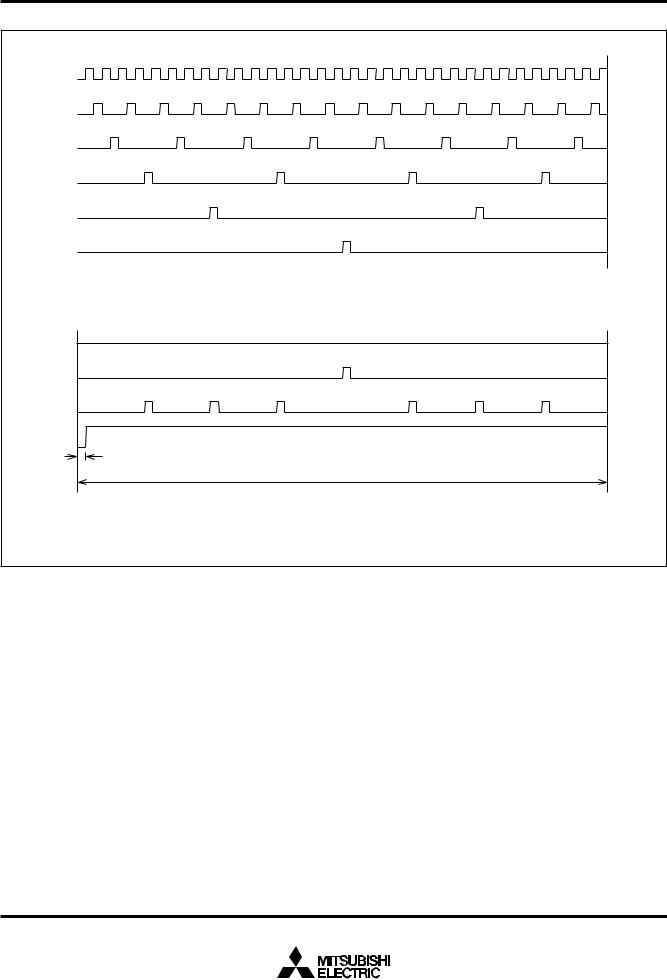
MITSUBISHI MICROCOMPUTERS
M37210M3-XXXSP/FP, M37210M4-XXXSP, M37211M2-XXXSP M37210E4-XXXSP/FP, M37210E4SP/FP
SINGLE-CHIP 8-BIT CMOS MICROCOMPUTER for VOLTAGE SYNTHESIZER with ON-SCREEN DISPLAY CONTROLLER
|
1 |
3 |
5 |
7 |
9 |
|
19 |
|
|
|
|
39 |
|
|
|
|
59 |
|
Bit 5 |
|
|
|
|
|
|
|
|
|
|
|
|
|
|
|
|
|
|
Bit 4 |
|
2 |
|
6 |
10 |
14 |
18 |
22 |
26 |
30 |
34 |
38 |
42 |
46 |
50 |
54 |
58 |
62 |
|
|
|
||||||||||||||||
Bit 3 |
|
|
4 |
|
|
12 |
20 |
|
|
28 |
|
36 |
|
44 |
|
52 |
60 |
|
|
|
|
|
|
|
|
|
|
|
|
||||||||
Bit 2 |
|
|
|
|
8 |
|
|
|
24 |
|
|
40 |
|
|
|
|
56 |
|
|
|
|
|
|
|
|
|
|
|
|
|
|
|
|
||||
Bit 1 |
|
|
|
|
|
|
16 |
|
|
|
|
|
|
|
48 |
|
|
|
|
|
|
|
|
|
|
|
|
|
|
|
|
|
|
|
|
||
Bit 0 |
|
|
|
|
|
|
|
|
|
|
32 |
|
|
|
|
|
|
|
|
|
|
|
|
|
|
|
|
|
|
|
|
|
|
|
|
|
|
|
|
|
|
|
|
|
|
|
|
|
|
|
|
|
|
|
|
|
(a) Pulses showing the weight of each bit
0016 |
(0) |
0116 |
(1) |
0616 |
(24) |
3F16 |
(63) |
T = 64t |
PWM output t = 10μs T = 1024μs |
f (XIN) = 4MHz |
(b) Example of 6-bit PWM output
Fig. 13 6-bit PWM timing
18
Loading...