


 Loading...
MITSUBISHI MICROCOMPUTERS
M37207MF-XXXSP/FP, M37207M8-XXXSP M37207EFSP/FP
SINGLE-CHIP 8-BIT CMOS MICROCOMPUTER for VOLTAGE SYNTHESIZER and ON-SCREEN DISPLAY CONTROLLER
DESCRIPTION
The M37207MF-XXXSP/FP and M37207M8-XXXSP are single-chip microcomputers designed with CMOS silicon gate technology. It is housed in a 64-pin shrink plastic molded DIP or a 80-pin plastic molded QFP.
In addition to their simple instruction sets, the ROM, RAM and I/O addresses are placed on the same memory map to enable easy programming.
The M37207MF-XXXSP/FP has a PWM function and an OSD function, so it is useful for a channel selection system for TV. The features of the M37207EFSP/FP are similar to those of the M37207MFXXXSP/FP except that these chips have a built-in PROM which can be written electrically. The difference between M37207MF-XXXSP/
FP and M37207M8-XXXSP are the ROM size, RAM size, ROM size for display and kinds of character. Accordingly, the following descriptions will be for the M37207MF-XXXSP/FP unless otherwise noted.
FEATURES |
|
|
• Number of basic instructions .................................................... |
|
71 |
• Memory size ................................................................................. |
|
|
ROM ...................... |
32K bytes (M37207M8-XXXSP) |
|
|
62K bytes (M37207MF-XXXSP/FP, |
|
|
|
M37207EFSP/FP) |
RAM ...................... |
512 bytes (M37207M8-XXXSP) |
|
|
960 bytes (M37207MF-XXXSP/FP, |
|
|
|
M37207EFSP/FP) |
ROM correction memory |
............................ 64 bytes |
|
ROM for display |
....... 8K bytes (M37207M8-XXXSP) |
|
|
12K bytes (M37207MF-XXXSP/FP, |
|
|
|
M37207EFSP/FP) |
RAM for display |
........................................ |
144 bytes |
• Minimum instruction execution time |
|
|
........................................ 0.5 µs (at 8 MHz oscillation frequency) |
||
• Power source voltage .................................................. |
|
5 V ± 10 % |
• Subroutine nesting ............................................ |
|
128 levels (Max.) |
• Interrupts ...................................................... |
|
15 types, 14 vectors |
• 8-bit timers ................................................................................. |
|
6 |
• Programmable I/O ports |
|
|
(Ports P0, P1, P2, P30–P36, P4, P6) ....................................... |
47 |
|
• Input ports (Ports P70, P71) ....................................................... |
|
2 |
• Output ports (Ports P52–P56) |
..................................................... |
5 |
• 12 V withstand ports ................................................................. |
|
10 |
• LED drive ports .......................................................................... |
|
4 |
• Serial I/O ....................................... |
8-bit 1 channel (2 systems) |
|
• Multi-master I2C-BUS interface ............................... |
|
1 (3 systems) |
• Power dissipation |
|
|
In high-speed mode ........................................................ |
|
165 mW |
(at VCC = 5.5 V, 8 MHz oscillation frequency, CRT on) |
||
In low-speed mode ......................................................... |
|
0.33 mW |
(at VCC = 5.5 V, 32 kHz oscillation frequency) |
||
• A-D comparator (6-bit resolution) ................................ |
|
8 channels |
• PWM output circuit ...................................... |
|
14-bit 1, 8-bit 10 |
• Interrupt interval determination circuit |
........................................ 1 |
|
• ROM correction function .......................................... |
|
32 bytes 2 |
• CRT display function |
|
|
Number of display characters ............... |
|
24 characters 3 lines |
|
|
(16 lines maximum) |
Kinds of characters .................. |
256 kinds (M37207M8-XXXSP) |
|
384 kinds (M37207MF-XXXSP/FP, |
||
|
|
M37207EFSP/FP) |
Character display area .......................................... |
|
12 16 dots |
Kinds of character sizes ................................................. |
|
4 kinds |
Kinds of character colors (It can be specified by the character) |
||
maximum 15 kinds (R, G, B, I) |
|
|
Kinds of character background colors (It can be specified by the character) |
||
maximum 7 kinds (R, G, B) |
|
|
1/2-character unit color specification is possible. |
||
Kinds of raster colors (maximum 15 kinds) |
||
Display position |
|
|
Horizontal .................................................................. |
|
64 levels |
Vertical .................................................................... |
|
128 levels |
Bordering (horizontal and vertical) |
|
|
Wipe function |
|
|
Scanning line double count mode display is possible.
APPLICATION
TV
MITSUBISHI MICROCOMPUTERS
M37207MF-XXXSP/FP, M37207M8-XXXSP
M37207EFSP/FP
SINGLE-CHIP 8-BIT CMOS MICROCOMPUTER for VOLTAGE SYNTHESIZER and ON-SCREEN DISPLAY CONTROLLER
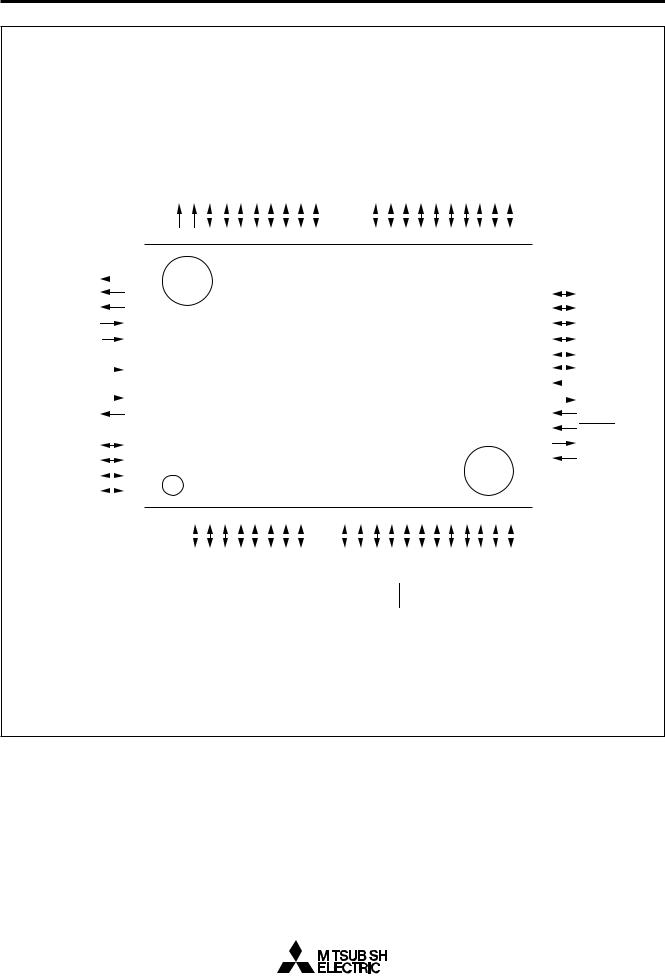
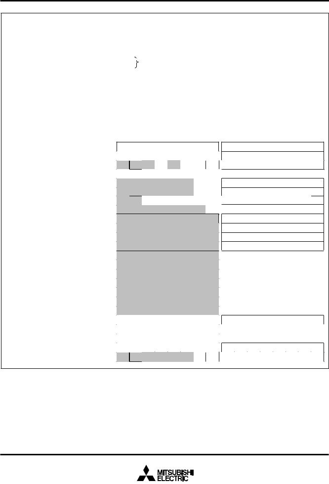
PIN CONFIGURATION (TOP VIEW)
OSC1/P70/AD4 |
|
|
|
VCC |
1 |
|
64 |
||
|
|
|
|
|
OSC2/P71/AD5 |
2 |
|
63 |
HSYNC |
|
|
|
|
|
P36/INT2/AD2 |
3 |
|
62 |
VSYNC |
P35/AD1 |
|
|
|
R/P52 |
4 |
|
61 |
||
P34/INT1 |
|
|
|
G/P53 |
5 |
|
60 |
||
|
|
|
|
|
D-A/AD3 |
6 |
|
59 |
B/P54 |
P60/PWM0 |
|
|
|
I/P55/TIM1 OVERFLOW |
7 |
|
58 |
||
|
|
|
|
OUT/P56 |
P61/PWM1 |
8 |
|
57 |
|
|
|
|
|
|
P62/PWM2 |
9 |
|
56 |
P00 |
|
|
XXXSP,-M37207MF M37207EFSP |
|
|
P31 |
17 |
48 |
P10 |
|
P63/PWM3 |
10 |
|
55 |
P01 |
P64/PWM4 |
11 |
|
54 |
P02 |
P65/PWM5 |
12 |
|
53 |
P03 |
P66/PWM6 |
13 |
|
52 |
P04 |
P67/PWM7 |
|
|
|
P05 |
14 |
|
51 |
||
|
|
|
|
|
P33/TIM3 |
15 |
|
50 |
P06 |
P32/TIM2/AD6 |
|
|
|
P07 |
16 |
|
49 |
||
P30 |
|
-M37207M8 |
|
P11 |
|
|
|||
|
|
|||
18 |
47 |
|||
P47/SRDY1 /PWM8 |
|
|
|
P12 |
19 |
|
46 |
||
P46/SIN1/PWM9 |
|
|
|
P13 |
20 |
|
45 |
||
P45/SCLK1/SCL1 |
|
|
|
P14 |
21 |
|
44 |
||
P44/SOUT1/SDA1 |
|
XXXSP |
|
P15 |
22 |
43 |
|||
P43/SRDY2/SCL2/AD7 |
|
|
P16 |
|
23 |
42 |
|||
P42/SIN2/SDA2/AD8 |
|
|
|
P17 |
24 |
|
41 |
||
P41/SCLK2/SCL3/XCOUT |
|
|
|
P20 |
25 |
|
40 |
||
P40/SOUT2/SDA3/XCIN |
|
|
|
P21 |
26 |
|
39 |
||
CNVSS |
|
|
|
P22 |
27 |
|
38 |
||
φ |
|
|
|
P23 |
28 |
|
37 |
||
|
|
|
|
P24 |
RESET |
29 |
|
36 |
|
XIN |
|
|
|
P25 |
30 |
|
35 |
||
XOUT |
|
|
|
P26 |
31 |
|
34 |
||
|
|
|
|
|
VSS |
32 |
|
33 |
P27 |
|
|
|
|
|
Outline 64P4B
2
MITSUBISHI MICROCOMPUTERS
M37207MF-XXXSP/FP, M37207M8-XXXSP
M37207EFSP/FP
SINGLE-CHIP 8-BIT CMOS MICROCOMPUTER for VOLTAGE SYNTHESIZER and ON-SCREEN DISPLAY CONTROLLER
PIN CONFIGURATION (TOP VIEW)
NC |
|
65 |
|
B/P54 |
|
66 |
|
G/P53 |
|
67 |
|
R/P52 |
|
68 |
|
|
|
VSYNC |
69 |
|
|
HSYNC |
70 |
|
|
NC |
71 |
|
|
VCC |
72 |
NC |
|
73 |
|
OSC1/P70/AD4 |
|
74 |
|
OSC2/P71/AD5 |
|
75 |
|
NC |
|
76 |
|
P36/INT2/AD2 |
|
77 |
|
P35/AD1 |
|
78 |
|
P34/INT1 |
|
79 |
|
D-A/AD3 |
|
80 |
|
|
|
|
|
NC I/P55/TIM1 OVERFLOW |
|
OUT/P56 |
P00 |
P01 |
P02 |
P03 |
P04 |
|
P05 |
|
P06 |
P07 |
|
NC |
|
NC |
|
NC |
|
P10 |
|
P11 |
|
P12 |
|
P13 |
|
P14 |
|
P15 |
|
P16 |
P17 |
|
P20 |
|
P21 |
|||||||||
|
|
|
|
|
|
|
|
|
|
|
|
|
|
|
|
|
|
|
|
|
|
|
|
|
|
|
|
|
|
|
|
|
|
|
|
|
|
|
|
|
|
|
|
|
|
|
64 |
|
63 |
|
62 |
|
61 |
|
60 |
|
59 |
|
58 |
|
57 |
|
56 |
|
55 |
|
54 |
|
53 |
|
52 |
|
51 |
|
50 |
|
49 |
|
48 |
|
47 |
|
46 |
|
45 |
|
44 |
|
43 |
|
42 |
|
41 |
|
|
|
|
|
|
|
|
|
|
|
|
|
|
|
|
|
|
|
|
|
|
|
|
|
|
|
|
|
|
|
|
|
|
|
|
|
|
|
|
|
|
|
|
|
|
|
M37207MF-XXXFP, M37207EFFP
1 |
|
2 |
|
3 |
|
4 |
|
5 |
|
6 |
|
7 |
|
8 |
|
9 |
|
10 |
|
11 |
|
12 |
|
13 |
|
14 |
|
15 |
|
16 |
|
17 |
|
18 |
|
19 |
|
20 |
|
21 |
|
22 |
|
23 |
|
24 |
NC |
NC |
P60/PWM0 |
P61/PWM1 |
P62/PWM2 |
P63/PWM3 |
P64/PWM4 |
P65/PWM5 |
P66/PWM6 |
P67/PWM7 |
NC NC P33/TIM3 |
P32/TIM2/AD6 |
P31 |
P30 |
P47/SRDY1 /PWM8 |
P46/SIN1/PWM9 |
P45/SCLK1/SCL1 |
P44/SOUT1/SDA1 |
P43/SRDY2 /SCL2/AD7 |
P42/SIN2/SDA2/AD8 |
P41/SCLK2/SCL3/XCOUT P4φ/SOUT2/SDA3/XCIN |
|
NC |
40 |
|
|
NC |
39 |
|
|
P22 |
38 |
|
|
P23 |
37 |
|
|
P24 |
36 |
|
|
P25 |
35 |
|
|
P26 |
34 |
|
|
P27 |
33 |
|
|
VSS |
32 |
|
|
XOUT |
31 |
|
|
XIN |
30 |
|
|
RESET |
29 |
|
|
φ |
28 |
|
|
CNVSS |
27 |
|
|
NC |
26 |
|
|
NC |
25 |
|
|
|
Outline 80P6N-A |
NC: Unconnected |
|||
|
|
|
|
|
|
|
|
|
|
|
|
|
|
|
3

4
FUNCTIONAL BLOCK DIAGRAM of M37207M8-XXXSP
|
|
|
|
|
|
|
|
|
|
|
|
|
|
|
|
|
|
|
|
|
|
|
|
|
|
|
|
|
|
Input ports P70, P71 |
||
|
|
|
|
Clock |
Clock |
|
|
|
|
|
|
|
|
|
|
|
|
|
|
|
|
|
|
|
|
|
|
|
Clock input for CRT/ |
Clock output for CRT/ |
||
|
|
|
|
input |
output |
|
Timing output |
Reset input |
|
|
|
|
|
|
|
|
|
Sub-clock input |
Sub-clock output |
|||||||||||||
|
|
|
|
XIN |
XOUT |
|
|
φ |
|
|
|
|
RESET |
|
|
|
|
VCC VSS CNVSS |
|
|
|
|
OSC1 |
OSC2 |
||||||||
|
|
30 |
31 |
28 |
|
|
|
|
29 |
|
|
|
|
64 |
|
32 |
27 |
|
|
1 |
2 |
|
||||||||||
|
|
|
|
|
|
|
|
|
|
|
|
|
|
|
|
|
|
|
|
|
|
|
|
|
|
|
|
|
A-D comparator |
|
|
|
|
|
|
|
|
Clock |
|
|
|
|
|
|
|
|
|
|
|
|
|
|
|
|
|
|
|
|
|
|
|
||||
|
|
|
|
generating |
|
|
|
|
|
|
|
|
|
|
|
|
|
|
|
|
|
|
|
|
|
|
|
|
|
|||
|
|
|
|
|
circuit |
|
|
|
|
|
Data bus |
|
|
|
|
|
|
|
|
|
|
TIM2 |
|
Timer count source |
|
|
|
|
|
|||
|
|
|
|
|
|
|
|
|
|
|
|
|
|
|
|
|
|
|
|
|
|
|
|
|
|
|||||||
|
|
|
|
|
|
|
|
|
|
|
|
|
|
|
|
|
|
|
|
|
|
|
|
|
|
|
||||||
|
|
|
|
|
|
|
|
|
|
|
|
|
|
|
|
|
|
|
|
|
|
|
|
|
|
|
||||||
|
|
|
|
|
|
|
|
|
|
|
|
|
|
|
|
|
|
|
|
|
|
|
|
|
TIM3 |
|
|
|
|
|
|
|
|
|
|
XCIN |
|
|
|
|
|
|
|
|
|
|
|
|
|
|
|
|
|
|
|
|
selection circuit |
|
|
|
|
|
|||
|
|
|
|
|
|
(Note 1) |
|
|
|
|
|
|
|
|
|
(Note 2) |
|
|
|
|
|
|
|
|
|
|||||||
|
|
|
|
|
|
|
|
|
|
|
|
|
|
|
|
|
|
|
|
|
|
|
|
|
|
|
||||||
|
|
|
|
|
|
|
|
|
|
|
RAM |
Program Program |
|
|
|
ROM |
|
Timer 1 |
|
|
|
|
|
|||||||||
|
|
|
|
|
XCOUT |
|
|
|
960 bytes |
counter |
counter |
|
64 K bytes |
|
T1 (8) |
|
|
|
|
|
||||||||||||
|
|
|
|
|
|
|
|
|
|
|
|
|
|
PCH (8) |
PCL (8) |
|
|
|
|
|
|
Timer 2 |
|
|
|
|
|
|||||
|
|
|
|
|
|
|
|
|
|
|
|
|
|
|
|
|
|
|
|
|
|
|
|
|
||||||||
|
|
|
|
|
|
|
|
|
|
|
|
|
|
|
|
|
|
|
|
|
|
|
|
|
|
|
|
|
|
|
|
|
|
|
|
|
Address bus |
|
|
|
|
|
|
|
|
|
|
|
|
|
|
|
|
T2 (8) |
|
|
|
|
|
||||||
|
|
|
|
|
|
|
|
|
|
|
|
|
|
|
|
|
|
|
|
|
|
|
|
|
|
|||||||
|
|
|
|
|
|
|
|
|
|
|
|
|
|
|
|
|
|
|
|
|
|
|
|
|
|
|
Timer 3 |
|
|
|
|
|
|
|
|
|
|
|
|
|
|
|
|
|
|
|
|
|
|
|
|
|
|
|
|
|
|
|
|
T3 (8) |
|
|
|
|
|
|
|
|
|
|
|
|
|
|
|
|
|
|
|
|
|
|
|
|
|
|
|
|
|
|
|
|
Timer 4 |
Control signal |
|
|
||
|
|
|
|
|
|
|
|
|
|
|
|
|
|
|
|
|
|
|
|
|
|
|
|
|
|
|
|
|
||||
|
|
|
|
|
|
|
|
|
|
|
|
|
|
|
|
|
|
|
|
|
|
|
|
|
|
|
|
|||||
|
|
|
|
|
|
|
|
|
|
|
|
|
|
|
|
|
|
|
|
|
Index |
|
|
|
T4 (8) |
|
|
|||||
|
|
|
|
|
|
|
|
|
|
|
|
|
|
|
|
|
|
|
|
|
|
|
|
|
|
|
|
|
||||
|
|
|
8-bit |
Accumulator |
processor |
|
Index |
|
|
|
|
Stack |
|
|
|
|
|
|
|
|||||||||||||
|
|
|
|
|
|
|
|
|
|
|
|
|
|
|||||||||||||||||||
|
|
|
arithmetic |
|
|
A (8) |
status |
|
register |
|
|
register |
|
pointer |
|
Timer 5 |
Instruction |
|
|
|||||||||||||
|
|
|
|
and |
|
|
|
|
|
register |
|
X (8) |
|
|
|
Y (8) |
|
S (8) |
|
decoder |
|
|
||||||||||
|
|
|
|
|
|
|
|
|
|
|
|
|
|
|
T5 (8) |
|
|
|||||||||||||||
|
|
|
logical unit |
|
|
|
|
|
PS (8) |
|
|
|
|
|
|
|
|
|
|
|
|
|
|
|
|
CRT circuit |
|
|||||
|
|
|
|
|
|
|
|
|
|
|
|
|
|
|
|
|
|
|
|
|
|
|
|
|
||||||||
|
|
|
|
|
|
|
|
|
|
|
|
|
|
|
|
|
|
|
|
|
|
|
|
|
|
|
|
|
|
|
||
|
|
|
|
|
|
|
|
|
|
|
|
|
|
|
|
|
|
|
|
|
|
|
|
|
|
|
Timer 6 |
instruction |
|
|
||
|
|
|
|
|
|
|
|
|
|
|
|
|
|
|
|
|
|
|
|
|
|
|
|
|
|
|
|
|
||||
|
|
|
|
|
|
|
|
|
|
|
|
|
|
|
|
|
|
|
|
|
|
|
|
|
|
|
register (8) |
|
|
|||
|
|
|
|
|
|
|
|
|
|
|
|
|
|
|
|
|
|
|
|
|
|
|
|
|
|
|
T6 (8) |
|
|
|||
|
|
|
|
|
|
|
|
|
|
|
|
|
|
|
|
|
|
|
|
|
|
|
|
|
|
|
|
|
|
|
|
|
|
|
|
|
|
|
|
|
|
|
|
|
|
|
|
|
|
|
|
|
|
|
|
|
|
|
|
|
|
|
|
|
|
|
|
|
|
|
|
|
|
|
|
|
|
|
|
|
|
|
|
|
|
|
|
|
|
|
|
|
|
|
|
|
|
|
|
|
INT1 |
INT2 |
|
|
|
SI/O (8) |
|
|
Multi-master |
8-bit PWM circuit |
|||
|
A-D |
SOUT2 |
SCLK2 |
SIN2 |
SRDY2 SOUT1 SCLK1 |
SIN1 |
SRDY1 |
I2C-BUS Interface |
PWM7 PWM6 PWM5 PWM4 PWM3 |
PWM2 PWM1 |
PWM0 |
|||
|
SDA3 SCL3 SDA2 SCL2 SDA1 SCL1 |
|||||||||||||
|
comparator |
|||||||||||||
P0(8) |
P1 (8) |
|||||||||||||
P2 (8) |
|
P3 (7) |
|
|
|
|
P4 (8) |
|
P6 (8) |
|
P5 (5) |
|||
|
|
|
|
|
|
|
14-bit |
|
|
|
|
|
|
|
|
|
|
|
|
|
|
|
PWM circuit |
|
|
|
|
|
OUT I B G R |
|
|
|
|
|
|
|
|
|
|
|
|
|
|
|
VSYNC |
HSYNC |
|
49 50 51 52 53 54 55 56 41 42 43 44 45 46 47 48 33 34 35 36 37 38 39 40 |
3 |
4 |
5 |
15 16 17 18 |
6 |
26 25 24 23 22 21 20 19 |
14 13 12 11 10 |
9 |
8 |
7 |
57 58 59 60 61 |
62 |
63 |
||
I/O ports |
I/O ports |
I/O ports |
|
|
I/O ports |
D-A |
I/O ports P40–P47 |
I/O ports P60–P67 |
Output ports |
Sync |
|||||
P00–P07 |
P10–P17 |
P20–P27 |
|
|
P30–P36 |
|
|
|
|
|
|
P52–P56 |
input |
||
Note 1: M37207M8-XXXSP has a 512 bytes RAM.
Note 2: M37207M8-XXXSP has a 32 K bytes ROM.
SYNTHESIZER VOLTAGE for MICROCOMPUTER CMOS BIT-8 CHIP-SINGLE CONTROLLER DISPLAY SCREEN-ON and |
XXXSP-M37207M8 XXXSP/FP,-M37207MF M37207EFSP/FP |
MICROCOMPUTERS MITSUBISHI |

MITSUBISHI MICROCOMPUTERS
M37207MF-XXXSP/FP, M37207M8-XXXSP
M37207EFSP/FP
SINGLE-CHIP 8-BIT CMOS MICROCOMPUTER for VOLTAGE SYNTHESIZER and ON-SCREEN DISPLAY CONTROLLER
FUNCTIONS
Parameter |
|
|
|
|
|
|
Functions |
|
Number of basic instructions |
|
|
|
|
71 |
|
|
|
|
|
|
|
|
|
|||
Instruction execution time |
|
|
|
|
0.5 ms (the minimum instruction execution time, at 8 MHz oscillation fre- |
|||
|
|
|
|
|
quency) |
|||
|
|
|
|
|
|
|||
Clock frequency |
|
|
|
|
8 MHz (maximum) |
|||
|
|
|
|
|
|
|||
Memory size |
ROM |
|
M37207M8-XXXSP |
32 K bytes |
||||
|
|
|
|
|
||||
|
|
|
M37207MF-XXXSP/FP, |
64 K bytes |
||||
|
|
|
M37207EFSP/FP |
|
|
|
|
|
|
|
|
|
|
||||
|
RAM |
|
M37207M8-XXXSP |
512 bytes |
||||
|
|
|
|
|
|
|
|
|
|
|
|
M37207MF-XXXSP/FP, |
960 bytes |
||||
|
|
|
M37207EFSP/FP |
|
|
|
|
|
|
|
|
|
|||||
|
ROM correction memory |
64 bytes |
||||||
|
|
|
|
|
||||
|
CRT ROM |
|
M37207M8-XXXSP |
8K bytes |
||||
|
|
|
M37207MF-XXXSP/FP, |
12K bytes |
||||
|
|
|
M37207EFSP/FP |
|
|
|
|
|
|
CRT RAM |
|
|
|
144 bytes |
|||
Input/Output ports |
P00–P07 |
|
|
I/O |
8-bit 1 (CMOS input/output structure) |
|||
|
P10–P17 |
|
|
I/O |
8-bit 1 (CMOS input/output structure) |
|||
|
|
|
|
|
|
|||
|
P20–P27 |
|
|
I/O |
8-bit 1 (CMOS input/output structure) |
|||
|
P30, P31 |
|
|
I/O |
2-bit 1 (CMOS input/output structure) |
|||
|
P32–P36 |
|
|
I/O |
5-bit 1 (N-channel open-drain output structure, can be used as external |
|||
|
|
|
|
|
clock input pins, A-D input pins, INT input pins) |
|||
|
P40–P47 |
|
|
I/O |
8-bit 1 (N-channel open-drain output structure, can be used as serial I/O |
|||
|
|
|
|
|
pins, A-D input pins, PWM output pins, multi-master I2C-BUS interface, |
|||
|
|
|
|
|
sub-clock I/O pins) |
|||
|
P52–P56 |
|
|
Output |
5-bit 1 (CMOS output structure, can be used as CRT output pins, an |
|||
|
|
|
|
|
external clock output pin) |
|||
|
P60–P67 |
|
|
I/O |
8-bit 1 (N-channel open-drain output structure, can be used as PWM |
|||
|
|
|
|
|
output) |
|||
|
|
|
|
|
|
|||
|
P70, P70 |
|
|
Input |
2-bit 1 (can be used as CRT display clock I/O pins, analog input pins) |
|||
|
|
|
|
|
|
|||
Serial I/O |
|
|
|
|
8-bit 1 (2 systems) |
|||
|
|
|
|
|
|
|||
Multi-master I2C-BUS interface |
|
|
|
|
1 (3 systems) |
|||
A-D comparator |
|
|
|
|
8 channels (6-bit resolution) |
|||
PWM output circuit |
|
|
|
|
14-bit 1, 8-bit 10 |
|||
Timers |
|
|
|
|
8-bit timer 6 |
|||
ROM correction function |
|
|
|
|
32 bytes 2 |
|||
Subroutine nesting |
|
|
|
|
128 levels (maximum) |
|||
Interrupt interval determination circuit |
|
|
|
1 |
|
|
|
|
Interrupt |
|
|
|
|
External interrupt 2, Internal timer interrupt 6, Serial I/O interrupt 1, |
|||
|
|
|
|
|
CRT interrupt 1, Multi-master I2C-BUS interface interrupt 1, |
|||
|
|
|
|
|
f(XIN)/4096 interrupt 1, VSYNC interrupt 1, BRK interrupt 1 |
|||
|
|
|
|
|
|
|||
Clock generating circuit |
|
|
|
|
2 built-in circuits (externally connected to a ceramic resonator or a quartz- |
|||
|
|
|
|
|
crystal oscillator) |
|||
|
|
|
|
|
|
|
|
|
|
|
|
|
|
|
|
|
|
|
|
|
|
|
|
|
|
|
5

MITSUBISHI MICROCOMPUTERS
M37207MF-XXXSP/FP, M37207M8-XXXSP
M37207EFSP/FP
SINGLE-CHIP 8-BIT CMOS MICROCOMPUTER for VOLTAGE SYNTHESIZER and ON-SCREEN DISPLAY CONTROLLER
FUNCTIONS (continued)
|
Parameter |
|
|
|
Functions |
||
Power source voltage |
|
5 V ± 10 % |
|||||
|
|
|
|
|
|||
Power dissipation |
In high-speed |
CRT ON |
165 mW typ. (at oscillation frequency f(XIN) = 8 MHz, fOSC = 8 MHz) |
||||
|
mode |
|
|
|
|
|
|
|
CRT OFF |
82.5 mW typ. (at oscillation frequency f(XIN) = 8 MHz) |
|||||
|
|
||||||
|
|
|
|
|
|||
|
In low-speed |
CRT OFF |
0.33 mW typ. (at oscillation frequency fCLK = 32 kHz, f(XIN) = stopped) |
||||
|
mode |
|
|
|
|
|
|
|
|
|
|
|
|||
|
In stop mode |
|
1.1 mW (maximum) |
||||
|
|
|
|
|
|||
Operating temperature range |
|
–10 °C to 70 °C |
|||||
|
|
|
|
|
|||
Device structure |
|
|
CMOS silicon gate process |
||||
|
|
|
|
||||
Package |
M37207MF-XXXSP, M37207M8-XXXSP |
64-pin shrink plastic molded DIP |
|||||
|
M37207EFSP |
|
|
|
|
|
|
|
|
|
|
||||
|
M37207MF-XXXFP, M37207EFFP |
80-pin plastic molded QFP |
|||||
|
|
|
|
||||
|
Number of display characters |
24 characters 3 lines (maximum 16 lines by software) |
|||||
|
|
|
|
||||
CRT display |
Character display area |
12 16 dots |
|||||
function |
Kinds of |
M37207M8-XXXSP |
256 Kinds |
||||
|
|||||||
|
characters |
M37207MF-XXXSP/FP, |
384 Kinds |
||||
|
|
||||||
|
|
M37207EFSP/FP |
|
|
|
|
|
|
|
|
|
|
|||
|
Kinds of character sizes |
4 kinds |
|||||
|
|
|
|
||||
|
Kinds of character colors |
Maximum 15 kinds (R, G, B, I); can be specified by the character |
|||||
|
|
|
|
||||
|
Display position (horizontal, vertical) |
64 levels (horizontal) 128 levels (vertical) |
|||||
|
|
|
|
|
|
|
|
|
|
|
|
|
|
|
|
|
|
|
|
|
|
|
|
|
|
|
|
|
|
|
|
6

MITSUBISHI MICROCOMPUTERS
M37207MF-XXXSP/FP, M37207M8-XXXSP
M37207EFSP/FP
SINGLE-CHIP 8-BIT CMOS MICROCOMPUTER for VOLTAGE SYNTHESIZER and ON-SCREEN DISPLAY CONTROLLER
PIN DESCRIPTION
Pin |
Name |
Input/ |
|
|
|
Functions |
|
Output |
|
|
|
||||
|
|
|
|
|
|
||
|
|
|
|
||||
VCC, VSS |
Power source |
|
Apply voltage of 5 V ± 10 % (typical) to VCC and AVCC, and 0 V to VSS. |
||||
|
|
|
|
||||
CNVSS |
CNVSS |
|
Connected to VSS. |
||||
______ |
Reset input |
|
To enter the reset state, the reset input pin must be kept at a “L” for 2 ms or more (under |
||||
RESET |
Input |
||||||
|
|
|
normal VCC conditions). |
||||
|
|
|
If more time is needed for the quartz-crystal oscillator to stabilize, this “L” condition should |
||||
|
|
|
be maintained for the required time. |
||||
|
|
|
|
||||
XIN |
Clock input |
Input |
This chip has an internal clock generating circuit. To control generating frequency, an |
||||
|
|
|
external ceramic resonator or a quartz-crystal oscillator is connected between pins XIN and |
||||
XOUT |
Clock output |
Output |
XOUT. If an external clock is used, the clock source should be connected to the XIN pin and |
||||
|
|
|
the XOUT pin should be left open. |
||||
P00–P07 |
I/O port P0 |
I/O |
Port P0 is an 8-bit I/O port with direction register allowing each I/O bit to be individually |
||||
programmed as input or output. At reset, this port is set to input mode. The output structure |
|||||||
|
|
|
|||||
|
|
|
is CMOS output. See notes at end of table for full details of port P0 functions. |
||||
|
|
|
|
||||
P10–P17 |
I/O port P1 |
I/O |
Port P1 is an 8-bit I/O port and has basically the same functions as port P0. The output |
||||
|
|
|
structure is CMOS output. |
||||
|
|
|
|
||||
P20–P27 |
I/O port P2 |
I/O |
Port P2 is an 8-bit I/O port and has basically the same functions as port P0. The output |
||||
|
|
|
structure is CMOS output. |
||||
P30, P31 |
I/O port P3 |
I/O |
Ports P30, P31 are 2-bit I/O ports and have basically the same functions as port P0. The |
||||
|
|
|
output structure is CMOS output. |
||||
P32/TIM2/ |
I/O port P3 |
I/O |
Ports P32–P36 are 5-bit I/O ports and have basically the same functions as port P0. The |
||||
AD6, |
|
|
output structure is N-channel open-drain output. |
||||
P33/TIM3, |
|
|
|
|
|
|
|
Analog input |
Input |
Pins P32, P35, P36 are also used as analog input pins AD6, AD1 and AD2 respectively. |
|||||
P34/INT1, |
|||||||
External clock |
Input |
Pins P32, P33 are also used as external clock input pins TIM2, TIM3 respectively. |
|||||
|
|||||||
P35/AD1, |
input |
|
|
|
|
|
|
|
|
|
|
||||
P36/INT2/ |
External interrupt |
Input |
Pins P34, P36 are also used as external interrupt input pins INT1, INT2. |
||||
AD2 |
input |
|
|
|
|
|
|
|
|
|
|
||||
P40/SOUT2/ |
I/O port P4 |
I/O |
Port P4 is an 8-bit I/O port and has basically the same functions as port P0. The output |
||||
SDA3/XCIN, |
|
|
structure is N-channel open-drain output. |
||||
P41/SCLK2/ |
Serial I/O data |
I/O |
Pins P40, P42, P44, P46 are also used as serial I/O data input/output pins SOUT2, SIN2, |
||||
SCL3/ |
input/output |
|
SOUT1, SIN1 respectively. The output structure is N-channel open-drain output. |
||||
XCOUT, P42/ |
|
|
|
|
|
|
|
Serial I/O synchro- |
I/O |
Pins P41, P45 are also used as serial I/O synchronous clock input/output pins SCLK2, SCLK1 |
|||||
SIN2/SDA2/ |
|||||||
nous clock input/ |
|
respectively. |
|||||
AD8, |
|
||||||
output |
|
|
|
|
|
||
_____ |
|
|
|
|
|
||
P43/SRDY2/ |
|
|
_____ _____ |
||||
Serial I/O receive |
Output |
Pins P43, P47 are also used as serial I/O receive enable signal output pins SRDY2, SRDY1 |
|||||
SCL2/AD7, |
|||||||
enable signal output |
|
respectively. The output structure is N-channel open-drain output. |
|||||
|
|
||||||
P44/SOUT1/ |
|
|
|
||||
Multi-master I2C- |
I/O |
Pins P40–P45 are also used as SDA3, SCL3, SDA2, SCL2, SDA1, SCL1 respectively |
|||||
SDA1, |
BUS interface |
|
when multi-master I2C-BUS interface is used. The output structure is N-channel open- |
||||
P45/SCLK1/ |
|
|
drain output. |
||||
SCL1, |
|
|
|
|
|
|
|
Sub-clock input |
Input |
Pin P40 is also used as sub-clock input pin XCIN. |
|||||
|
|||||||
P46/SIN1/ |
Sub-clock output |
Output |
Pin P41 is also used as sub-clock output pin XCOUT. The output structure is N-channel |
||||
PWM9, |
|||||||
|
|
open-drain output. |
|||||
_____ |
|
|
|||||
P47/SRDY1/ |
|
|
|
|
|
|
|
Analog input |
Input |
Pins P42, P43 are also used as analog input pins AD8, AD7 respectively. |
|||||
PWM8 |
|||||||
PWM output |
Output |
Pins P46, P47 are also used as PWM output pins PWM9, PWM8 respectively. The output |
|||||
|
|||||||
|
|
|
structure is N-channel open-drain output. |
||||
|
|
|
|
|
|
|
|
|
|
|
|
|
|
|
|
|
|
|
|
|
|
|
|
7

MITSUBISHI MICROCOMPUTERS
M37207MF-XXXSP/FP, M37207M8-XXXSP
M37207EFSP/FP
SINGLE-CHIP 8-BIT CMOS MICROCOMPUTER for VOLTAGE SYNTHESIZER and ON-SCREEN DISPLAY CONTROLLER
PIN DESCRIPTION (continued)
Pin |
Name |
Input/ |
Functions |
|
Output |
||||
|
|
|
||
R/P52, |
Output port |
Output |
Ports P52–P56 are 5-bit output ports. The output structure is CMOS output. |
|
G/P53, |
P5 |
|
|
|
B/P54, |
CRT output |
Output |
Pins P52–P56 are also used as CRT output pins R, G, B, I, OUT respectively. The output structure |
|
I/P55/TIM1 |
|
|
is CMOS output. |
|
OVERFLOW, |
Timer 1 overflow |
Output |
Pin P55 is also used as timer 1 overflow signal output pin TIM1 OVERFLOW. The output structure is |
|
|
||||
OUT/P56 |
signal output |
|
CMOS output. |
|
|
|
|
|
|
P60/PWM– |
I/O port P6 |
I/O |
Port P6 is an 8-bit I/O port and has basically the same functions as port P0. The output structure is |
|
P67/PWM7 |
|
|
N-channel open-drain output. |
|
|
|
|
|
|
|
PWM output |
Output |
Pins P60–P67 are also used as PWM output pins PWM0–PWM7. The output structure is CMOS |
|
|
|
|
output. |
|
|
|
|
|
|
OSC1/P70/ |
Input port P7 |
Input |
Ports P70, P71 are 2-bit input port. |
|
AD4, |
|
|
|
|
Clock input |
Input |
Pin P70 is also used as CRT display clock input pin OSC1. |
||
|
||||
OSC2/P71/ |
for CRT |
|
|
|
AD5 |
display |
|
|
|
|
|
|
|
|
|
Clock output |
Output |
Pin P71 is also used as CRT display clock output pin OSC2. The output structure is CMOS output. |
|
|
for CRT |
|
|
|
|
display |
|
|
|
|
|
|
|
|
|
Analog input |
Input |
Pins P70, P71 are also used as analog input pins AD4, AD5 respectively. |
|
|
|
|
|
|
HSYNC |
HSYNC input |
Input |
This is a horizontal synchronous signal input for CRT display. |
|
VSYNC |
VSYNC input |
Input |
This is a vertical synchronous signal input for CRT display. |
|
f |
Timing |
Output |
This is a timing output pin. This pin has reset-out output function. The output structure is CMOS |
|
|
output |
|
output. |
|
D-A/AD3 |
DA output |
Output |
This is an output pin for 14-bit PWM. |
|
|
Analog input |
Input |
The D-A pin is also used as analog input pin AD3. |
|
|
|
|
|
Note : As shown in the memory map (Figure 5), port P0 is accessed as a memory at address 00C016 of zero page. Port P0 has the port P0 direction register (address 00C116 of zero page) which can be used to program each bit as an input (“0”) or an output (“1”). The pins programmed as “1” in the direction register are output pins. When pins are programmed as “0,” they are input pins. When pins are programmed as output pins, the output data are written into the port latch and then output. When data is read from the output pins, the output pin level is not read but the data of the port latch is read. This allows a previously-output value to be read correctly even if the output “L” voltage has risen, for example, because a light emitting diode was directly driven. The input pins float, so the values of the pins can be read. When data is written into the input pin, it is written only into the port latch, while the pin remains in the floating state.
8

MITSUBISHI MICROCOMPUTERS
M37207MF-XXXSP/FP, M37207M8-XXXSP M37207EFSP/FP
SINGLE-CHIP 8-BIT CMOS MICROCOMPUTER for VOLTAGE SYNTHESIZER and ON-SCREEN DISPLAY CONTROLLER
Ports P00–P07, P10–P17, P20–P27, P30, P31, D-A
Direction register
Data bus |
Port latch |
Ports P46, P47, P60–P67
Direction register
Data bus |
Port latch |
Ports P32–P36, P42–P45
Direction register
Data bus |
Port latch |
CMOS output
Ports P00–P07, P10–P17,
P20–P27, P30, P31, D-A
Note : D-A pin is also used as
AD3.
N-channel open-drain output


 Ports P46, P47, P60–P67
Note : Each port is also used as follows:
P46 : SIN1/PWM9
_____
P47 : SRDY1/PWM8
P60–P67 : PWM0–PWM7
N-channel open-drain output
 Ports P32–P36, P42–P45
Note : Each port is also used as follows:
P32 : TIM2/AD6
P33 : TIM3
P34 : INT1
P35 : AD1
P36 : INT2/AD2
P42 : SIN2/SDA2/AD8
_____
P43 : SRDY2/SCL2/AD7
P44 : SOUT1/SDA1
P45 : SCLK1/SCL1
Fig. 1. I/O Pin Block Diagram (1)
9

MITSUBISHI MICROCOMPUTERS
M37207MF-XXXSP/FP, M37207M8-XXXSP M37207EFSP/FP
SINGLE-CHIP 8-BIT CMOS MICROCOMPUTER for VOLTAGE SYNTHESIZER and ON-SCREEN DISPLAY CONTROLLER
HSYNC, VSYNC
Internal circuit


R, G, B, I, OUT,
φ
P52–P55,
Internal circuit 
Schmidt input
HSYNC, VSYNC
CMOS output
P52–P55, φ
Note : Each port is also used as follows:
P52 : R
P53 : G
P54 : B
P55 : I/TIM1
P56 : OUT
Fig. 2. I/O Pin Block Diagram (2)
10
MITSUBISHI MICROCOMPUTERS
M37207MF-XXXSP/FP, M37207M8-XXXSP M37207EFSP/FP
SINGLE-CHIP 8-BIT CMOS MICROCOMPUTER for VOLTAGE SYNTHESIZER and ON-SCREEN DISPLAY CONTROLLER
FUNCTIONAL DESCRIPTION
Central Processing Unit (CPU)
This microcomputer uses the standard 740 Family instruction set. Refer to the table of 740 Family addressing modes and machine instructions or the SERIES 740 <Software> User’s Manual for details on the instruction set.
Machine-resident 740 Family instructions are as follows:
The FST, SLW instruction cannot be used.
The MUL, DIV, WIT and STP instructions can be used.
CPU Mode Register
The CPU mode register contains the stack page selection bit and internal system clock selection bit. The CPU mode register is allocated at address 00FB16.
CPU Mode Register
b7 b6 b5 b4b3 b2 b1 b0
1 |
0 |
0 |
CPU mode register (CPUM) (CM) [Address 00FB 16]
B |
Name |
|
Functions |
After reset R W |
|
0, 1 Processor mode bits |
b1 b0 |
0 |
R W |
||
|
(CM0, CM1) |
0 0: Single-chip mode |
|
|
|
|
|
0 |
1: |
|
|
|
|
1 |
0: Not available |
|
|
|
|
1 |
1: |
|
|
2Stack page selection bit (CM2) (See note 1)
3 Fix these bits to “1.”
4Internal system clock output selection bit (CM4) (See note 2)
5XCOUT drivability selection bit (CM5)
0: 0 page |
1 |
R W |
1: 1 page |
|
|
|
1 |
R W |
0: Output is stopped |
1 |
R W |
1: Internal system |
|
|
clock φ output |
|
|
0: LOW drive |
1 |
R W |
1: HIGH drive |
|
|
6 |
Main Clock (XIN–XOUT) 0: Oscillating |
0 |
R W |
|
|
stop bit |
1: Stopped |
|
|
|
(CM6) |
|
|
|
|
|
|
|
|
7 |
Internal system clock 0: XIN–XOUT selected |
0 |
R W |
|
|
selection bit |
(high-speed mode) |
|
|
|
(CM7) |
|
|
|
|
1: XCIN–XCOUT selected |
|
|
|
|
|
|
|
|
|
|
(high-speed mode) |
|
|
Notes 1: This bit is set to “1” after the reset release. 2: The internal system clock φ stops at HIGH.
Fig. 3. CPU Mode Register
11

MITSUBISHI MICROCOMPUTERS
M37207MF-XXXSP/FP, M37207M8-XXXSP M37207EFSP/FP
SINGLE-CHIP 8-BIT CMOS MICROCOMPUTER for VOLTAGE SYNTHESIZER and ON-SCREEN DISPLAY CONTROLLER
MEMORY
Special Function Register (SFR) Area
The special function register (SFR) area in the zero page contains control registers such as I/O ports and timers.
RAM
RAM is used for data storage and for stack area of subroutine calls and interrupts.
ROM
ROM is used for storing user programs as well as the interrupt vector area.
RAM for Display
RAM for display is used for specifying the character codes and colors to display.
Interrupt Vector Area
The interrupt vector area contains reset and interrupt vectors.
Zero Page
The 256 bytes from addresses 000016 to 00FF16 are called the zero page area. The internal RAM and the special function registers (SFR) are allocated to this area.
The zero page addressing mode can be used to specify memory and register addresses in the zero page area. Access to this area with only 2 bytes is possible in the zero page addressing mode.
Special Page
The 256 bytes from addresses FF0016 to FFFF16 are called the special page area. The special page addressing mode can be used to specify memory addresses in the special page area. Access to this area with only 2 bytes is possible in the special page addressing mode.
ROM for Display |
|
ROM for display is used for storing character data. |
ROM Correction Memory (RAM) |
|
|
|
This is used as the program area for ROM correction. |
|
|
|
|
000016 |
|
|
|
|
|
|
|
|
|
|
|
|
|
RAM |
|
RAM |
00C016 |
|
|
|
(960 bytes) |
|
(512 bytes) |
|
SFR area |
|
for M37207MF |
|
for M37207M8 |
00FF16 |
|
|
|
|
|
01FF16 |
|
|
|
|
|
|
Not used |
|
|
|
|
020416 |
2 page register |
|
|
|
|
021B16 |
|
|
|
|
|
|
|
|
|
|
|
|
Not used |
|
|
|
|
02C016 |
|
|
|
|
|
02FF16 |
|
|
|
|
|
030016 |
|
|
|
|
|
033F16 |
|
|
|
|
|
04FF16 |
|
|
|
|
RAM |
|
Not used |
|
|
|
060016 |
|
|
|
|
|
for display |
|
|
|
|
|
|
|
|
|
|
|
(144 bytes) |
06D716 |
|
|
|
|
(See note) |
|
|
|
|
|
|
Not used |
|
|
|
|
|
|
|
|
|
|
|
080016 |
|
|
|
|
|
|
|
|
ROM |
|
ROM |
800016 |
|
|
|
|
|
||
(62 K bytes) |
(32 K bytes) |
|
|
||
for M37207MF |
for M37207M8 |
FF0016 |
|
||
|
|
|
|
|
|
|
|
|
|
FFDE16 |
Interrupt vector area |
|
|
|
|
FFFF16 |
|
|
|
|
|
|
|
|
1000016 |
|
Zero page |
ROM |
|
for display |
||
|
||
ROM |
(8 K bytes) |
|
for display |
for M37207M8 |
|
(12 K bytes) |
11FFF16 |
|
for M37207MF |
||
|
||
|
12FFF16 |
ROM correction memory (64 bytes)
Block 1: addresses 02C0 16 to 02DF16
Block 2: addresses 02E0 16 to 02FF16
 Special page
1FFFF16
Not used
Note: Refer to Table 9. Contents of CRT display RAM.
Fig. 4. Memory Map
12
MITSUBISHI MICROCOMPUTERS
M37207MF-XXXSP/FP, M37207M8-XXXSP M37207EFSP/FP
SINGLE-CHIP 8-BIT CMOS MICROCOMPUTER for VOLTAGE SYNTHESIZER and ON-SCREEN DISPLAY CONTROLLER
■SFR Area (addresses C016 to DF16)
< Bit allocation >
: 
 Function bit
Name : 

 : No function bit
0 : Fix this bit to “0” (do not write “1”)
1 : Fix this bit to “1” (do not write “0”)
Address |
Register |
Bit allocation |
b7
<State immediately after reset>
0: “0” immediately after reset
1: “1” immediately after reset
?: Undefined immediately after reset
State immediately after reset
b0 |
b7 |
b0 |
C016
C116
C216
C316
C416
C516
C616
C716
C816
C916
CA16
CB16
CC16
CD16
CE16
CF16
D016
D116
D216
D316
D416
D516
D616
D716
D816
D916
DA16
DB16
DC16
DD16
DE16
DF16
Port P0 (P0) |
|
|
|
|
|
|
|
|
|
|
|
|
|
|
? |
|
|
|
|
Port P0 direction register (D0) |
|
|
|
|
|
|
|
|
|
|
|
|
|
0016 |
|
|
|
||
Port P1 (P1) |
|
|
|
|
|
|
|
|
|
|
|
|
|
|
? |
|
|
|
|
Port P1 direction register (D1) |
|
|
|
|
|
|
|
|
|
|
|
|
|
0016 |
|
|
|
||
Port P2 (P2) |
|
|
|
|
|
|
|
|
|
|
|
|
|
|
? |
|
|
|
|
Port P2 direction register (D2) |
|
|
|
|
|
|
|
|
|
|
|
|
|
0016 |
|
|
|
||
Port P3 (P3) |
|
|
|
|
|
|
|
|
|
0 |
? |
? |
? |
|
? |
? |
? |
? |
|
Port P3 direction register (D3) |
|
|
|
|
|
|
|
|
|
|
|
|
|
0016 |
|
|
|
||
Port P4 (P4) |
|
|
|
|
|
|
|
|
|
|
|
|
|
|
? |
|
|
|
|
Port P4 direction register (D4) |
|
|
|
|
|
|
|
|
|
|
|
|
|
|
? |
|
|
|
|
Port P5 (P5) |
|
|
|
|
|
|
|
|
|
0 |
? |
? |
? |
? |
? |
? |
? |
||
Port P5 control register (D5) |
|
|
|
|
|
|
|
|
|
|
|
|
|
0016 |
|
|
|
||
Port P6 (P6) |
|
|
|
|
|
|
|
|
|
|
|
|
|
|
? |
|
|
|
|
Port P6 direction register (D6) |
|
|
|
|
|
|
|
|
|
|
|
|
|
0016 |
|
|
|
||
DA-H register (DA-H) |
|
|
|
|
|
|
|
|
|
|
|
|
|
|
? |
|
|
|
|
DA-L register (DA-L) |
|
|
|
|
|
|
|
|
|
0 |
0 |
? |
? |
? |
? |
? |
? |
||
PWM0 register (PWM0) |
|
|
|
|
|
|
|
|
|
|
|
|
|
|
? |
|
|
|
|
PWM1 register (PWM1) |
|
|
|
|
|
|
|
|
|
|
|
|
|
|
? |
|
|
|
|
PWM2 register (PWM2) |
|
|
|
|
|
|
|
|
|
|
|
|
|
|
? |
|
|
|
|
PWM3 register (PWM3) |
|
|
|
|
|
|
|
|
|
|
|
|
|
|
? |
|
|
|
|
PWM4 register (PWM4) |
|
|
|
|
|
|
|
|
|
|
|
|
|
|
? |
|
|
|
|
PWM output control register 1 (PW) |
PW7 |
PW6 |
PW5 |
PW4 |
PW3 |
PW2 |
PW1 |
PW0 |
|
|
|
|
|
0016 |
|
|
|
||
PWM output control register 2 (PN) |
|
|
|
PN4 |
PN3 |
PN2 |
PN1 |
PN0 |
|
|
|
|
|
0016 |
|
|
|
||
Interrupt interval determination register (??) |
|
|
|
|
|
|
|
|
|
|
|
|
|
|
? |
|
|
|
|
Interrupt interval determination control register (RE) |
|
|
RE5 |
RE4 |
RE3 |
RE2 |
RE1 |
RE0 |
|
|
|
|
|
0016 |
|
|
|
||
I2C data shift register (S0) |
D7 |
D6 |
D5 |
D4 |
D3 |
D2 |
D1 |
D0 |
|
|
|
|
|
|
? |
|
|
|
|
|
|
|
|
|
|
|
|
|
|
|
|
|
|
|
|
|
|||
SAD6 |
SAD5 |
SAD4 |
SAD3 |
SAD2 |
SAD1 |
SAD0 |
RBW |
|
|
|
|
|
0016 |
|
|
|
|||
I2C address register (S0D) |
|
|
|
|
|
|
|
|
|||||||||||
|
|
|
|
|
|
|
|
|
|
|
|
|
|
|
|
||||
MST |
TRX |
BB |
PIN |
AL |
AAS |
AD0 |
LRB |
|
0 |
0 |
|
0 |
1 |
|
0 |
0 |
0 |
? |
|
I2C status register (S1) |
|
|
|
||||||||||||||||
|
|
|
|
|
|
|
|
|
|
|
|||||||||
I2C control register (S1D) |
BSEL1 |
BSEL0 |
10BIT |
ALS |
ESO |
BC2 |
BC1 |
BC0 |
|
|
|
|
|
0016 |
|
|
|
||
SAD |
|
|
|
|
|
|
|
|
|||||||||||
ACK |
ACK |
FAST |
CCR4 |
CCR3 |
CCR2 |
CCR1 |
CCR0 |
|
|
|
|
|
0016 |
|
|
|
|||
I2C clock control register (S2) |
|
|
|
|
|
|
|
|
|||||||||||
|
BIT |
MODE |
|
|
|
|
|
|
|
|
|
|
|
|
|
|
|
|
|
|
SM6 |
SM5 |
0 |
SM3 |
SM2 |
SM1 |
SM0 |
|
|
|
|
|
0016 |
|
|
|
|||
Serial I/O mode register (SM) |
|
|
|
|
|
|
|
|
|
||||||||||
Serial I/O regsiter (SIO) |
|
|
|
|
|
|
|
|
|
|
|
|
|
|
? |
|
|
|
|
Fig. 5. Memory Map of Special Function Register (SFR)
13
MITSUBISHI MICROCOMPUTERS
M37207MF-XXXSP/FP, M37207M8-XXXSP
M37207EFSP/FP
SINGLE-CHIP 8-BIT CMOS MICROCOMPUTER for VOLTAGE SYNTHESIZER and ON-SCREEN DISPLAY CONTROLLER
■ SFR Area (addresses E016 to FF16)
< Bit allocation> |
|
< State immediately after reset > |
|||||
|
|
|
: |
|
|
|
: “0” immediately after reset |
|
|
|
|
0 |
|||
|
|
|
Function |
bit |
|
|
|
|
|
|
|
|
|
||
Name |
: |
|
|
1 |
: “1” immediately after reset |
||
|
|
|
: No function bit |
|
|
: Undefined immediately |
|
|
|
|
|
|
|||
|
|
|
|
|
|||
|
? |
||||||
|
|
|
|
|
|
||
|
|
|
: Fix this bit to “0” |
|
|
after reset |
|
|
|
|
|
|
|||
0 |
|
|
|
|
|||
|
|
|
|
|
|||
|
|
|
(do not write “1”) |
|
|
|
|
|
|
: Fix this bit to “1” |
|
|
|
||
1 |
|
|
|
|
|||
|
|
|
(do not write “0”) |
|
|
|
|
Address |
Register |
|
E016 |
Horizontal register (HR) |
|
E116 |
Vertical register 1 (CV1) |
|
E216 |
Vertical register 2 (CV2) |
|
E316 |
Vertical register 3 (CV3) |
|
E416 |
Character size register (CS) |
|
E516 |
Border selection register (MD) |
|
E616 |
Color register 0 (CO0) |
|
E716 |
Color register 1 (CO1) |
|
E816 |
Color register 2 (CO2) |
|
E916 |
Color register 3 (CO3) |
|
EA16 |
CRT control register 1 (CC) |
|
EB16 |
Display block counter (CBC) |
|
EC16 |
CRT port control register (CRTP) |
|
ED16 |
Wipe mode register (SL) |
|
EE16 |
Wipe start register (??) |
|
EF16 |
A-D control register 1 (ADM) |
|
F016 |
Timer 1 (TM1) |
|
F116 |
Timer 2 (TM2) |
|
F216 |
Timer 3 (TM3) |
|
F316 |
Timer 4 (TM4) |
|
F416 |
Timer mode register 1 (TMR1) |
|
F516 |
Timer mode register 2 (TMR2) |
|
F616 |
PWM5 register (PWM5) |
|
F716 |
PWM6 register (PWM6) |
|
F816 |
PWM7 register (PWM7) |
|
F916 |
PWM8 register (PWM8) |
|
FA16 |
PWM9 register (PWM9) |
|
FB16 |
CPU mode register (CPUM) |
|
FC16 |
Interrupt request register 1 (IREQ1) |
|
FD16 |
Interrupt request register 2 (IREQ2) |
|
FE16 |
Interrupt control register 1 (ICON1) |
|
FF16 |
Interrupt control register 2 (ICON2) |
|
b7 |
|
Bit allocation |
|
b0 |
State immediately after reset |
|||||||||
|
|
|
|
|
b7 |
|
|
|
|
|
|
b0 |
||
0 |
|
HR5 HR4 HR3 HR2 HR1 HR0 |
|
|
|
0016 |
|
|
|
|||||
|
CV16 CV15 CV14 CV13 CV12 CV11 CV10 |
0 |
? |
? |
? |
? |
? |
? |
? |
|||||
|
|
|
|
|
|
|
||||||||
|
CV26 CV25 CV24 CV23 CV22 CV21 CV20 |
0 |
? |
? |
? |
? |
? |
? |
? |
|||||
|
|
|
|
|
|
|
||||||||
|
CV36 CV35 CV34 CV33 CV32 CV31 CV30 |
0 |
? ? ? ? ? ? ? |
|||||||||||
|
|
|
|
|
|
|
||||||||
CS7 |
|
CS31 CS30 CS21 CS20 CS11 CS10 |
0 |
0 |
? |
? ? ? ? ? |
||||||||
|
|
MD31 MD30 MD21 MD20 MD11 MD10 |
0 |
0 |
? |
? |
? |
? |
? |
? |
||||
CO07 CO06 CO05 CO04 CO03 CO02 CO01CO00 |
|
|
|
0016 |
|
|
|
|||||||
CO17 CO16 CO15 CO14 CO13 CO12 CO11CO11 |
|
|
|
0016 |
|
|
|
|||||||
CO27 CO26 CO25 CO24 CO23 CO22 CO21CO22 |
|
|
|
0016 |
|
|
|
|||||||
CO37 CO36 CO35 CO34 CO33 CO32 CO31CO33 |
|
|
|
0016 |
|
|
|
|||||||
0 |
CC6 CC5 CC4 CC3 CC2 CC1 CC0 |
|
|
|
0016 |
|
|
|
||||||
|
|
|
|
|
|
|
|
|
|
0016 |
|
|
|
|
B |
G |
R |
I |
R/G/B |
VSYC |
HSYC |
|
|
|
0016 |
|
|
|
|
|
SL6 |
SL5 |
SL4 SL3 |
SL2 |
SL1 |
SL0 |
|
|
|
0016 |
|
|
|
|
|
|
|
|
|
|
|
|
|
|
0016 |
|
|
|
|
|
|
|
ADM4 |
ADM2ADM1 ADM0 |
0 |
0 |
0 |
? |
0 |
0 |
0 |
0 |
||
|
|
|
|
|
|
|
||||||||
|
|
|
|
|
|
|
|
|
|
FF16 |
|
|
|
|
|
|
|
|
|
|
|
|
|
|
0716 |
|
|
|
|
FF16
|
|
|
|
|
|
|
|
|
|
0716 |
|
TMR17 |
TMR16 |
TMR15 |
TMR14 |
TMR13 |
TMR12 |
TMR11 |
TMR10 |
0016 |
|
|
TMR27 |
TMR26 |
TMR25 |
TMR24 |
TMR23 |
TMR22 |
TMR21 |
TMR20 |
|
0016 |
?
|
|
|
|
|
|
|
|
|
|
? |
|
|
|
|
|
|
|
|
|
|
|
|
|
|
? |
|
|
|
|
|
|
|
|
|
|
|
|
|
|
? |
|
|
|
|
|
|
1 |
1 |
|
0 |
0 |
0 |
0 |
1 |
? |
1 |
1 |
0 |
0 |
CM7 CM6 CM5 |
CM2 |
1 |
||||||||||||
|
|
|
|
|
|
|
CK0 |
|
|
|
|
|||
|
IICR VSCR CRTRTM4R TM3R TM2R TM1R |
|
|
|
0016 |
|
|
|
||||||
0 |
TM56R MSRCK0 |
|
S1R |
IT2R |
IT1R |
|
|
|
0016 |
|
|
|
||
|
IICE VSCE CRTE TM4E TM3E TM2E TM1E |
|
|
|
0016 |
|
|
|
||||||
TM56C |
0 TM56E MSE |
0 |
SIE |
IT2E |
IT1E |
|
|
|
0016 |
|
|
|
||
Fig. 6. Memory Map of Special Function Register (SFR)
14
MITSUBISHI MICROCOMPUTERS
M37207MF-XXXSP/FP, M37207M8-XXXSP
M37207EFSP/FP
SINGLE-CHIP 8-BIT CMOS MICROCOMPUTER for VOLTAGE SYNTHESIZER and ON-SCREEN DISPLAY CONTROLLER
■SFR Area (addresses 20416 to 21B16)
< Bit allocation> |
|
<State immediately after reset > |
||||
|
|
: |
|
|
|
: “0” immediately after reset |
|
|
|
|
0 |
||
|
|
Function |
bit |
|
|
|
|
|
|
|
|
||
Name |
: |
|
|
|
: “1” immediately after reset |
|
|
|
1 |
||||
|
|
: No function bit |
|
|
: Undefined immediately |
|
|
|
|
|
|||
|
|
|
|
|||
|
? |
|||||
|
|
|
|
|
||
|
|
: Fix this bit to “0” |
|
|
after reset |
|
|
|
|
|
|||
0 |
|
|
|
|||
|
|
|
|
|||
|
|
(do not write “1”) |
|
|
|
|
|
|
|
|
|||
1 |
: Fix this bit to “1” |
|
|
|
||
|
|
(do not write “0”) |
|
|
|
|
Address |
Register |
Bit allocation |
State immediately after reset |
b0 |
|
b7 |
b0 |
b7 |
20416 Timer 5 (T5)
20516 Timer 6 (T6)
20616 Port control register (P7D)
20716 Serial I/O control register (SIC)
20816 CRT control register 2 (CBR)
20916 CRT clock selection register (OP)
20A16 A-D control register (ADC)
20B16 Timer mode register (TMR3)
20C16
20D16
20E16
20F16
21016
21116
21216
21316
21416
21516
21616
21716 ROM correction address 1 (high-order)
21816 ROM correction address 1 (low-order)
21916 ROM correction address 2 (high-order)
21A16 ROM correction address 2 (low-order)
21B16 ROM correction enable register (RCR)
|
|
|
P7D4 |
|
P7D2 P7D1 |
P7D0 |
SIC7 |
SIC8 |
SIC5 |
SIC4 |
SIC3 |
SIC2 SIC1 |
SIC0 |
|
|
|
|
|
CBR1 CBR0 |
|
0 |
|
|
|
|
OP1OP0 |
|
|
|
ADC5 ADC4 ADC3 ADC2 ADC1 ADC0 |
||||
|
|
|
|
|
|
TMR30 |
0 0 RC1RC0
0016
0016
0 0 0 0 0 0 ? ?
0016
0016
0016
0 0 ? ? ? ? ? ?
0016
?
?
?
?
?
?
?
?
?
?
?
0016
0016
0016
0016
? ? ? ? 0 0 0 0
Fig. 7. Memory Map of 2 Page Register
15

MITSUBISHI MICROCOMPUTERS
M37207MF-XXXSP/FP, M37207M8-XXXSP
M37207EFSP/FP
SINGLE-CHIP 8-BIT CMOS MICROCOMPUTER for VOLTAGE SYNTHESIZER and ON-SCREEN DISPLAY CONTROLLER
|
<Bit allocation> |
|
<State immediately after reset> |
|||||||||||||||||||||
|
|
|
|
|
|
|
|
|
|
|
|
|
|
|
|
: “0” immediately after reset |
||||||||
|
|
|
|
: |
|
|
|
|
|
|
|
|
|
|
0 |
|||||||||
|
|
|
|
Function bit |
|
|
|
|
|
|
|
|
|
|
|
|
||||||||
|
|
|
|
|
|
|
|
|
|
|
|
|
|
|
|
|||||||||
|
|
Name |
|
: |
|
|
|
|
|
|
|
|
|
|
1 |
: “1” immediately after reset |
||||||||
|
|
|
|
: No function bit |
|
|
|
: Undefined immediately |
||||||||||||||||
|
|
|
|
|
|
|
||||||||||||||||||
|
|
|
|
|
|
|
||||||||||||||||||
|
|
|
|
|
|
? |
||||||||||||||||||
|
|
|
|
|
|
|
|
|
|
|
|
|
|
|
||||||||||
|
|
|
|
: Fix this bit to “0” |
|
|
|
|
after reset |
|||||||||||||||
|
|
|
|
|
|
|
|
|||||||||||||||||
|
|
0 |
|
|
|
|
|
|||||||||||||||||
|
|
|
|
|
|
|
|
|
|
|
|
|
|
|
||||||||||
|
|
|
|
(do not write “1”) |
|
|
|
|
|
|
|
|
|
|
|
|
||||||||
|
|
|
|
|
|
|
|
|
|
|
|
|
|
|
||||||||||
|
|
1 |
: Fix this bit to “1” |
|
|
|
|
|
|
|
|
|
|
|
|
|||||||||
|
|
|
|
(do not write “0”) |
|
|
|
|
|
|
|
|
|
|
|
|
||||||||
Register |
|
|
|
|
Bit allocation |
|
|
|
State immediately after reset |
|||||||||||||||
|
b7 |
|
|
|
|
|
|
|
|
|
b0 |
|
b7 |
|
|
|
|
|
|
|
b0 |
|||
Processor status register (PS) |
|
|
|
|
|
|
|
|
|
|
|
|
|
|
|
|
|
|
|
|
|
|
|
|
|
N |
V |
T |
B |
D |
I |
Z |
C |
|
? |
|
? |
? |
? |
? |
1 |
? |
? |
|
|||||
Program counter (PCH) |
|
|
|
|
||||||||||||||||||||
|
|
|
|
|
|
|
|
|
|
|
|
|
|
|
Contents of address FFFF16 |
|
||||||||
Program counter (PCL) |
|
|
|
|
|
|
|
|
|
|
|
|
|
|
|
|
||||||||
|
|
|
|
|
|
|
|
|
|
|
|
|
|
|
Contents of address FFFE16 |
|
||||||||
|
|
|
|
|
|
|
|
|
|
|
|
|
|
|
|
|
||||||||
|
|
|
|
|
|
|
|
|
|
|
|
|
|
|
|
|
|
|
|
|
|
|
|
|
Fig. 8. Internal State of Processor Status Register and Program Counter at Reset |
|
|
|
|
|
|
|
|
|
|
|
|
||||||||||||
|
|
|
|
|
|
|
|
|
|
|
|
|
|
|
|
|
|
|
|
|
|
|
|
|
|
|
|
|
|
|
|
|
|
|
|
|
|
|
|
|
|
|
|
|
|
|
|
|
|
|
|
|
|
|
|
|
|
|
|
|
|
|
|
|
|
|
|
|
|
|
|
|
|
|
16

MITSUBISHI MICROCOMPUTERS
M37207MF-XXXSP/FP, M37207M8-XXXSP M37207EFSP/FP
SINGLE-CHIP 8-BIT CMOS MICROCOMPUTER for VOLTAGE SYNTHESIZER and ON-SCREEN DISPLAY CONTROLLER
INTERRUPTS
Interrupts can be caused by 15 different sources consisting of 3 external, 10 internal, 1 software, and reset. Interrupts are vectored interrupts with priorities as shown in Table 1. Reset is also included in the table because its operation is similar to an interrupt.
When an interrupt is accepted,
(1)The contents of the program counter and processor status register are automatically stored into the stack.
(2)The interrupt disable flag I is set to “1” and the corresponding interrupt request bit is set to “0.”
(3)The jump destination address stored in the vector address enters the program counter.
Other interrupts are disabled when the interrupt disable flag is set to “1.”
All interrupts except the BRK instruction interrupt have an interrupt request bit and an interrupt enable bit. The interrupt request bits are in interrupt request registers 1 and 2 and the interrupt enable bits are in interrupt control registers 1 and 2. Figures 10 to 13 show the inter- rupt-related registers.
Interrupts other than the BRK instruction interrupt and reset are accepted when the interrupt enable bit is “1,” interrupt request bit is “1,” and the interrupt disable flag is “0.” The interrupt request bit can be set to “0” by a program, but not set to “1.” The interrupt enable bit can be set to “0” and “1” by a program.
Reset is treated as a non-maskable interrupt with the highest priority.
Figure 9 shows interrupt control.
Table 1. Interrupt Vector Addresses and Priority
Interrupt Causes
(1)VSYNC and CRT interrupts
The VSYNC interrupt is an interrupt request synchronized with the vertical sync signal.
The CRT interrupt occurs after character block display to the CRT is completed.
(2)INT1, INT2 interrupts
With an external interrupt input, the system detects that the level of a pin changes from “L” to “H” or from “H” to “L,” and generates an interrupt request. The input active edge can be selected by bits 3 and 4 of the interrupt interval determination control register
(address 00D816) : when this bit is “0,” a change from “L” to “H” is detected; when it is “1,” a change from “H” to “L” is detected. Note that all bits are cleared to “0” at reset.
(3)Timer 1, 2, 3 and 4 interrupts
An interrupt is generated by an overflow of timer 1, 2, 3 or 4.
(4)Serial I/O interrupt
This is an interrupt request from the clock synchronous serial
I/O function.
Interrupt Source |
Priority |
Vector Addresses |
Remarks |
|
|
|
|
Reset |
1 |
FFFF16, FFFE16 |
Non-maskable |
|
|
|
|
CRT interrupt |
2 |
FFFD16, FFFC16 |
|
|
|
|
|
INT1 interrupt |
3 |
FFFB16, FFFA16 |
Active edge selectable |
|
|
|
|
INT2 interrupt |
4 |
FFF916, FFF816 |
Active edge selectable |
|
|
|
|
Timer 4 interrupt |
5 |
FFF716, FFF616 |
|
|
|
|
|
f(XIN)/4096 interrupt |
6 |
FFF516, FFF416 |
|
|
|
|
|
VSYNC interrupt |
7 |
FFF316, FFF216 |
Active edge selectable |
|
|
|
|
Timer 3 interrupt |
8 |
FFF116, FFF016 |
|
|
|
|
|
Timer 2 interrupt |
9 |
FFEF16, FFEE16 |
|
|
|
|
|
Timer 1 interrupt |
10 |
FFED16, FFEC16 |
|
|
|
|
|
Serial I/O interrupt |
11 |
FFEB16, FFEA16 |
|
|
|
|
|
Multi-master I2C-BUS interface interrupt |
12 |
FFE716, FFE616 |
|
Timer 5 · 6 interrupt |
13 |
FFE316, FFE216 |
Source switch by software (See note) |
|
|
|
|
BRK instruction interrupt |
14 |
FFDF16, FFDE16 |
Non-maskable (software interrupt) |
Note : Switching a source during a program causes an unnecessary interrupt. Therefore, set a source at initializing of program.
17

MITSUBISHI MICROCOMPUTERS
M37207MF-XXXSP/FP, M37207M8-XXXSP
M37207EFSP/FP
SINGLE-CHIP 8-BIT CMOS MICROCOMPUTER for VOLTAGE SYNTHESIZER and ON-SCREEN DISPLAY CONTROLLER
(5)f(XIN)/4096 interrupt
This interrupt occurs regularly with a f(XIN)/4096 period. Set bit 0 of the PWM output control register 1 to “0.”
(6)Multi-master I2C-BUS interface interrupt
This is an interrupt request related to the multi-master I2C-BUS interface.
(7)Timer 5 · 6 interrupt
An interrupt is generated by an overflow of timer 5 or 6. Their priorities are same, and can be switched by software.
(8)BRK instruction interrupt
This software interrupt has the least significant priority. It does not have a corresponding interrupt enable bit, and it is not affected by the interrupt disable flag I (non-maskable).
Interrupt request bit 
Interrupt enable bit 
Interrupt disable flag I 
BRK instruction 
 Interrupt request
Reset
Fig. 9. Interrupt Control
18
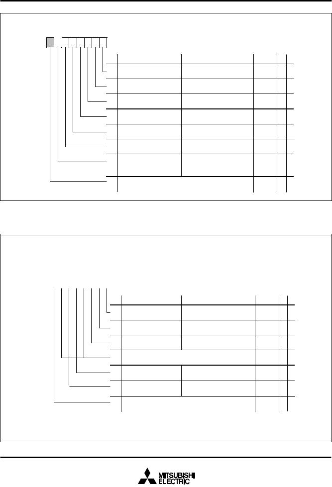
MITSUBISHI MICROCOMPUTERS
M37207MF-XXXSP/FP, M37207M8-XXXSP
M37207EFSP/FP
SINGLE-CHIP 8-BIT CMOS MICROCOMPUTER for VOLTAGE SYNTHESIZER and ON-SCREEN DISPLAY CONTROLLER
Interrupt Request Register 1
b7 b6 b5b4 b3 b2 b1 b0
Interrupt request register 1 (IREQ1) [Address 00FC 16]
B |
Name |
|
Functions |
After reset |
R W |
||
0 |
Timer 1 interrupt |
0 |
: No interrupt request issued |
0 |
R |
|
|
|
request bit |
(TM1R) |
1 |
: Interrupt request issued |
|
|
|
1 |
Timer 2 interrupt |
0 |
: No interrupt request issued |
0 |
R |
|
|
|
request bit |
(TM2R) |
1 |
: Interrupt request issued |
|
|
|
2 |
Timer 3 interrupt |
0 |
: No interrupt request issued |
0 |
R |
|
|
|
request bit |
(TM3R) |
1 |
: Interrupt request issued |
|
|
|
3 |
Timer 4 interrupt |
0 |
: No interrupt request issued |
0 |
R |
|
|
|
request bit |
(TM4R) |
1 |
: Interrupt request issued |
|
|
|
4 |
CRT interrupt |
|
0 |
: No interrupt request issued |
0 |
R |
|
|
request bit |
(CRTR) |
1 |
: Interrupt request issued |
|
|
|
5 |
VSYNC interrupt |
0 |
: No interrupt request issued |
0 |
R |
|
|
|
request bit |
(VSCR) |
1 |
: Interrupt request issued |
|
|
|
6 |
Multi-master I2C-BUS |
0 |
: No interrupt request issued |
0 |
R |
|
|
|
interface interrupt |
1 |
: Interrupt request issued |
|
|
|
|
|
request bit |
(IICR) |
|
|
|
|
|
7 Nothing is assigned. This bit is a write disable bit. |
0 |
R — |
|||||
|
When this bit is read out, the value is “0.” |
|
|
|
|||
Fig. 10. Interrupt Request Register 1
Interrupt Request Register 2
b7 b6 b5 b4b3 b2 b1 b0 |
|
|
|
|
|
|
|
|||||||
0 |
|
|
|
|
|
|
|
Interrupt request register 2 (IREQ2) [Address 00FD 16] |
|
|
||||
|
|
|
|
|
|
|
|
|
|
|
|
|
|
|
|
|
|
|
|
|
|
|
B |
Name |
|
Functions |
After reset |
R W |
|
|
|
|
|
|
|
|
|
0 |
INT1 interrupt |
0 |
: No interrupt request issued |
0 |
R |
|
|
|
|
|
|
|
|
|
|
request bit (ITIR) |
1 |
: Interrupt request issued |
|
|
|
|
|
|
|
|
|
|
|
1 |
INT2 interrupt |
0 |
: No interrupt request issued |
0 |
R |
|
|
|
|
|
|
|
|
|
|
request bit (IT2R) |
1 |
: Interrupt request issued |
|
|
|
|
|
|
|
|
|
|
|
2 |
Serial I/O interrupt |
0 |
: No interrupt request issued |
0 |
R |
|
|
|
|
|
|
|
|
|
|
request bit (SIR) |
1 |
: Interrupt request issued |
|
|
|
|
|
|
|
|
|
|
|
3,6 |
Nothing is assigned. These bits are write disable bits. |
0 |
R |
— |
||
|
|
|
|
|
|
|
|
|
When these bits are read out, the values are “0.” |
|
|
|
||
|
|
|
|
|
|
|
|
4 |
f(XIN)/4096 interrupt |
0 |
: No interrupt request issued |
0 |
R |
|
|
|
|
|
|
|
|
|
|
request bit (MSR) |
1 |
: Interrupt request issued |
|
|
|
|
|
|
|
|
|
|
|
5 |
Timer 5 • 6 interrupt |
0 |
: No interrupt request issued |
0 |
R |
|
|
|
|
|
|
|
|
|
|
request bit (TM56R) |
1 |
: Interrupt request issued |
|
|
|
|
|
|
|
|
|
|
|
7 |
Fix this bit to “0.” |
|
|
0 |
R W |
|
|
|
|
|
|
|
|
|
|
|
|
|
|
|
|
: “0” can be set by software, but “1” cannot be set.
Fig. 11. Interrupt Request Register 2
19

MITSUBISHI MICROCOMPUTERS
M37207MF-XXXSP/FP, M37207M8-XXXSP
M37207EFSP/FP
SINGLE-CHIP 8-BIT CMOS MICROCOMPUTER for VOLTAGE SYNTHESIZER and ON-SCREEN DISPLAY CONTROLLER
Interrupt Control Register 1
b7 b6 b5 b4 b3 b2 b1b0
Interrupt control register 1 (ICON1) [Address 00FE16]
B |
Name |
|
Functions |
After reset |
R W |
|
0 |
Timer 1 interrupt |
0 |
: Interrupt disabled |
0 |
R |
W |
|
enable bit (TM1E) |
1 |
: Interrupt enabled |
|
|
|
1 |
Timer 2 interrupt |
0 |
: Interrupt disabled |
0 |
R |
W |
|
enable bit (TM2E) |
1 |
: Interrupt enabled |
|
|
|
2 |
Timer 3 interrupt |
0 |
: Interrupt disabled |
0 |
R |
W |
|
enable bit (TM3E) |
1 |
: Interrupt enabled |
|
|
|
3 |
Timer 4 interrupt |
0 |
: Interrupt disabled |
0 |
R |
W |
|
enable bit (TM4E) |
1 |
: Interrupt enabled |
|
|
|
4 |
CRT interrupt enable |
0 |
: Interrupt disabled |
0 |
R |
W |
|
bit (CRTE) |
1 |
: Interrupt enabled |
|
|
|
5 |
VSYNC interrupt enable |
0 |
: Interrupt disabled |
0 |
R |
W |
|
bit (VSCE) |
1 |
: Interrupt enabled |
|
|
|
6 |
Multi-master I2C-BUS |
0 |
: Interrupt disabled |
0 |
R |
W |
|
interface interrupt |
1 |
: Interrupt enabled |
|
|
|
|
enable bit (IICE) |
|
|
|
|
|
7 |
Nothing is assigned. This bit is a write disable |
0 |
R |
— |
||
|
bit. When this bit is read out, the value is “0.” |
|
|
|
||
|
|
|
|
|
|
|
Fig. 12. Interrupt Control Register 1
Interrupt Control Register 2
b7 b6 b5 b4 b3 b2 b1b0
0 |
0 |
Interrupt control register 2 (ICON2) [Address 00FF16]
B |
Name |
|
Functions |
After reset |
R W |
|
0 |
INT1 interrupt |
0 |
: Interrupt disabled |
0 |
R |
W |
|
enable bit (IT1E) |
1 |
: Interrupt enabled |
|
|
|
1 |
INT2 interrupt enable |
0 |
: Interrupt disabled |
0 |
R |
W |
|
bit (IT2E) |
1 |
: Interrupt enabled |
|
|
|
2 |
Serial I/O interrupt |
0 |
: Interrupt disabled |
0 |
R |
W |
|
enable bit (SIE) |
1 |
: Interrupt enabled |
|
|
|
3, 6 Fix these bits to “0.” |
|
|
0 |
R |
W |
|
4 |
f(XIN)/4096 interrupt |
0 |
: Interrupt disabled |
0 |
R |
W |
|
enable bit (MSE) |
1 |
: Interrupt enabled |
|
|
|
5 |
Timer 5 • 6 interrupt |
0 |
: Interrupt disabled |
0 |
R |
W |
|
enable bit (TM56E) |
1 |
: Interrupt enabled |
|
|
|
7 |
Timer 5 • 6 interrupt |
0 |
: Timer 5 |
0 |
R |
W |
|
switch bit (TM56C) |
1 |
: Timer 6 |
|
|
|
Fig. 13. Interrupt Control Register 2
20
MITSUBISHI MICROCOMPUTERS
M37207MF-XXXSP/FP, M37207M8-XXXSP M37207EFSP/FP
SINGLE-CHIP 8-BIT CMOS MICROCOMPUTER for VOLTAGE SYNTHESIZER and ON-SCREEN DISPLAY CONTROLLER
TIMERS
The M37267M6-XXXSP has 6 timers: timer 1, timer 2, timer 3, timer
4, timer 5 and timer 6. All timers are 8-bit timers with the 8-bit timer latch. The timer block diagram is shown in Figure 17 .
0 .
All of the timers count down and their divide ratio is 1/(n+1), where n is the value of timer latch. By writing a count value to the corresponding timer latch (addresses 00F016 to 00F316 : timers 1 to 4, addresses
020C16 and 020D16 : timers 5 and 6), the value is also set to a timer, simultaneously.
The count value is decremented by 1. The timer interrupt request bit is set to “1” by a timer overflow at the next count pulse after the count value reaches “0016.”
(1) Timer 1
Timer 1 can select one of the following count sources:
•f(XIN)/16 or f(XCIN)/16
•f(XIN)/4096 or f(XCIN)/4096
•f(XCIN)
•External clock from the TIM2 pin
The count source of timer 1 is selected by setting bits 5 and 0 of timer mode register 1 (address 00F416). Either f(XIN) or f(XCIN) is selected by bit 7 of the CPU mode register.
Timer 1 interrupt request occurs at timer 1 overflow.
(2) Timer 2
Timer 2 can select one of the following count sources:
•f(XIN)/16 or f(XCIN)/16
•Timer 1 overflow signal
•External clock from the TIM2 pin
The count source of timer 2 is selected by setting bits 4 and 1 of timer mode register 1 (address 00F416). Either f(XIN) or f(XCIN) is selected by bit 7 of the CPU mode register. When timer 1 overflow signal is a count source for timer 2, timer 1 functions as an 8-bit prescaler.
Timer 2 interrupt request occurs at timer 2 overflow.
(5) Timer 5
Timer 5 can select one of the following count sources:
•f(XIN)/16 or f(XCIN)/16
•f(XCIN)
•Timer 4 overflow signal
The count source of timer 3 is selected by setting bit 6 of timer mode register 1 (address 00F416) and bit 7 of timer mode register 2 (address 00F516). Either f(XIN) or f(XCIN) is selected by bit 7 of the CPU mode register.
Timer 5 interrupt request occurs at timer 5 overflow.
(6) Timer 6
Timer 6 can select one of the following count sources:
•f(XIN)/16 or f(XCIN)/16
•Timer 5 overflow signal
The count source of timer 6 is selected by setting bit 7 of timer mode register 1 (address 00F416). Either f(XIN) or f(XCIN) is selected by bit 7 of the CPU mode register. When timer 5 overflow signal is a count source for timer 6, timer 5 functions as an 8-bit prescaler.
Timer 6 interrupt request occurs at timer 6 overflow.
At reset, timers 3 and 4 are connected by hardware and “FF16” is automatically set in timer 3; “0716” in timer 4. The f(XIN) /16 is selected as the timer 3 count source. The internal reset is released by timer 4 overflow in this state and the internal clock is connected.
At execution of the STP instruction, timers 3 and 4 are connected by hardware and “FF16” is automatically set in timer 3; “0716” in timer 4.
However, the f(XIN) /16 is not selected as the timer 3 count source. So set bit 0 of timer mode register 2 (address 00F516) to “0” before execution of the STP instruction (f(XIN) /16 is selected as timer 3 count source). The internal STP state is released by timer 4 overflow in this state and the internal clock is connected.
As a result of the above procedure, the program can start under a stable clock.
: When bit 7 of the CPU mode register (CM7) is “1,” f(XIN) becomes f(XCIN).
The timer-related registers is shown in Figures 14 to 16.
(3) Timer 3
Timer 3 can select one of the following count sources:
•f(XIN)/16 or f(XCIN)/16
•External clock from the TIM3 pin
The count source of timer 3 is selected by setting bit 0 of timer mode register 2 (address 00F516). Either f(XIN) or f(XCIN) is selected by bit
7 of the CPU mode register.
Timer 3 interrupt request occurs at timer 3 overflow.
(4) Timer 4
Timer 4 can select one of the following count sources:
•f(XIN)/16 or f(XCIN)/16
•f(XIN)/2 or f(XCIN)/2
•Timer 3 overflow signal
The count source of timer 3 is selected by setting bits 1 and 4 of timer mode register 2 (address 00F516). Either f(XIN) or f(XCIN) is selected by bit 7 of the CPU mode register. When timer 3 overflow signal is a count source for timer 4, the timer 3 functions as an 8-bit prescaler.
Timer 4 interrupt request occurs at timer 4 overflow.
21
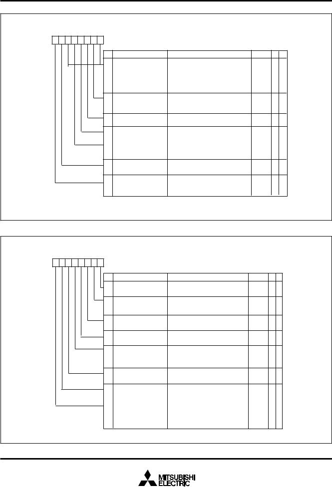
MITSUBISHI MICROCOMPUTERS
M37207MF-XXXSP/FP, M37207M8-XXXSP
M37207EFSP/FP
SINGLE-CHIP 8-BIT CMOS MICROCOMPUTER for VOLTAGE SYNTHESIZER and ON-SCREEN DISPLAY CONTROLLER
Timer Mode Register 1
b7 b6 b5b4 b3 b2 b1 b0
Timer mode register 1 (TMR1) [Address 00F416]
B Name
0Timer 1 count source selection bit 1 (TMR10, TMR15)
1Timer 2 count source selection bit 1 (TMR11)
2Timer 1 count stop bit (TMR12)
3Timer 2 count stop bit (TMR13)
4Timer 2 count source selection bit 2 (TMR14)
6Timer 5 count source selection bit 2 (TMR16)
7Timer 6 internal count source selection bit (TMR17)
Functions |
After reset R W |
|
b5 b0 |
0 |
R W |
0 0: f(XIN)/16 or f(XCIN)/16 (See note) |
|
|
01: f(XIN)/4096 or f(XCIN)/4096 (See note)
10: f(XcIN)
1 1: External clock from TIM2 pin
0: Count source selected by bit 4 of TM1 |
0 |
R |
W |
1: External clock from TIM2 pin |
|
|
|
0: Count start |
0 |
R |
W |
1: Count stop |
|
|
|
0: Count start |
0 |
R |
W |
1: Count stop |
|
|
|
0: f(XIN)/16 or f(XCIN)/16 (See note) |
0 |
R |
W |
1: Timer 1 overflow |
|
|
|
0: Timer 2 overflow |
0 |
R |
W |
1: Timer 4 overflow |
|
|
|
0: f(XIN)/16 or f(XCIN)/16 (See note) |
0 |
R |
W |
1: Timer 5 overflow |
|
|
|
Note: Either f(XIN) or f(XCIN) is selected by bit 7 of the CPU mode register.
Fig. 14. Timer Mode Register 1
Timer Mode Register 2
b7 b6 b5b4 b3 b2 b1 b0
Timer mode register 2 (TMR2) [Address 00F516]
B Name
0Timer 3 count source selection bit (TMR20)
1Timer 4 count source selection bit 2 (TMR21)
2Timer 3 count stop bit (TMR22)
3Timer 4 count stop bit (TMR23)
4Timer 4 count source selection bit 1 (TMR24)
5Timer 5 count stop bit (TMR25)
6Timer 6 count stop bit (TMR26)
7Timer 5 count source selection bit 1 (TMR27)
|
Functions |
After reset R |
W |
|
0 |
: f(XIN)/16 or f(XCIN)/16 (See note) |
0 |
R |
W |
1 |
: External clock from TIM3 pin |
|
|
|
0 |
: Timer 3 overflow signal |
0 |
R |
W |
1 |
: f(XIN)/16 or f(XCIN)/16 (See note) |
|
|
|
0: Count start |
0 |
R |
W |
|
1: Count stop |
|
|
|
|
0: Count start |
0 |
R |
W |
|
1: Count stop |
|
|
|
|
0: Count source selected by bit 1 |
0 |
R |
W |
|
|
of TMR2 |
|
|
|
1 |
: f(XIN)/2 or f(XCIN)/2 (See note) |
|
|
|
0: Count start |
0 |
R |
W |
|
1: Count stop |
|
|
|
|
0: Count start |
0 |
R |
W |
|
1: Count stop |
|
|
|
|
0: Count source selected by bit 0 |
0 |
R |
W |
|
|
of TMR3 |
|
|
|
1:Count source selected by bit 6 of TMR1
Note: Either f(XIN) or f(XCIN) is selected by bit 7 of the CPU mode register.
Fig. 15. Timer Mode Register 2
22

MITSUBISHI MICROCOMPUTERS
M37207MF-XXXSP/FP, M37207M8-XXXSP
M37207EFSP/FP
SINGLE-CHIP 8-BIT CMOS MICROCOMPUTER for VOLTAGE SYNTHESIZER and ON-SCREEN DISPLAY CONTROLLER
Timer Mode Register 3
b7 b6 b5b4 b3 b2 b1 b0
Timer mode register 3 (TMR3) [Address 020B16]
B |
Name |
|
Functions |
After reset R |
W |
||
0 |
Timer 5 count source |
0 |
: f(XIN)/16 or f(XCIN)/16 (See note) |
0 |
R |
W |
|
|
selection bit 3 |
1 |
: f(XCIN) |
|
|
|
|
|
(TMR30) |
|
|
|
|
|
|
1 |
Nothing is assigned. These bits are write disable bits. |
0 |
R |
— |
|||
to |
|||||||
When these bits are read out, the values are “0.” |
|
|
|
||||
7 |
|
|
|
||||
|
|
|
|
|
|
||
|
|
|
|
|
|
|
|
Note: Either f(XIN) or f(XCIN) is selected by bit 7 of the CPU mode register.
Fig. 16. Timer Mode Register 3
23

MITSUBISHI MICROCOMPUTERS
M37207MF-XXXSP/FP, M37207M8-XXXSP M37207EFSP/FP
SINGLE-CHIP 8-BIT CMOS MICROCOMPUTER for VOLTAGE SYNTHESIZER and ON-SCREEN DISPLAY CONTROLLER
8
XCIN |
CM7 |
|
|
|
|
|
|
|
|
|
1/4096 |
TMR15 |
|
Timer 1 latch (8) |
|
|
|
||
|
|
|
8 |
|
|
|
TMR15 |
|
|
XIN |
1/2 |
1/8 |
TMR10 |
Timer 1 (8) |
|
|
|
|
|
|
|
|
TMR12 |
8 |
|
|
|
|
|
|
|
|
TMR14 |
|
|
|
|
|
8 |
|
|
|
|
Timer 2 latch (8) |
|
|
|
|
8 |
TIM2 |
|
|
TMR11 |
Timer 2 (8) |
|
|
|
|
|
|
|
|
TMR13 |
8 |
|
|
|
|
|
|
|
|
|
8 |
TIM3 |
|
|
|
FF16 |
|
|
|
Timer 3 latch(8) |
|
|
|
|
|
|
|
|
|
|
8 |
|
|
|
TMR20 |
Timer 3 (8) |
|
|
|
|
|
|
|
|
TMR22 |
8 |
|
|
|
|
|
|
|
|
|
8 |
|
|
|
TMR21 |
0716 |
|
|
|
Timer 4 latch (8) |
|
|
|
|
|
|
|
|
|
|
8 |
|
|
|
TMR24 |
Timer 4 (8) |
|
|
|
|
|
|
|
|
TMR23 |
8 |
|
|
|
|
|
|
|
|
TMR16 |
8 |
|
|
|
|
Selection gate : Connected to black side at reset.
TMR1 : Timer mode register 1 TMR2 : Timer mode register 2 TMR3 : Timer mode register 3 CM : CPU mode register
|
Timer 5 latch (8) |
|
8 |
|
Timer 5 (8) |
TMR27 |
|
TMR30 TMR25 |
8 |
|
8 |
Timer 6 latch (8)
8


 Timer 6 (8) TMR17
TMR26 |
8 |
|
Data bus
Timer 1 interrupt request
Timer 2 interrupt request

 Reset
Reset
 STP instruction
Timer 3 interrupt request
Timer 4 interrupt request
Timer 5 interrupt request
Timer 6 interrupt request
Notes 1: HIGH pulse width of external clock inputs TIM2 and TIM3 needs 4 machine cycles or more.
2:When the external clock source is selected, timers 1, 2, and 3 are counted at a rising edge of input signal.
3:In the stop mode or the wait mode, external clock inputs TIM2 and TIM3 cannot be used.
Fig. 17. Timer Block Diagram
24
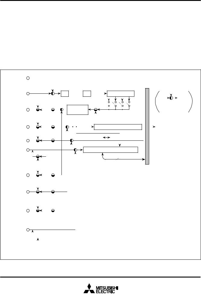
MITSUBISHI MICROCOMPUTERS
M37207MF-XXXSP/FP, M37207M8-XXXSP M37207EFSP/FP
SINGLE-CHIP 8-BIT CMOS MICROCOMPUTER for VOLTAGE SYNTHESIZER and ON-SCREEN DISPLAY CONTROLLER
SERIAL I/O
This microcomputer has a built-in serial I/O which can either transmit or receive 8-bit data serially in clock synchronous mode.
The serial I/O block diagram is shown in Figure 18. The synchronous
clock I/O pin (SCLK), and data I/O pins (SOUT, SIN), receive enable
____
signal output pin (SRDY) also function as port P4.
Bit 2 of the serial I/O mode register (address 00DE16) selects whether the synchronous clock is supplied internally or externally (from the pins SCLK1, SCLK2). When an internal clock is selected, bits 1 and 0 select whether f(XIN) or f(XCIN) is divided by 8, 16, 32, or 64. To use pins for serial I/O, set the corresponding bits of the port P4 direction register (address 00C916) to “0.”
The operation of the serial I/O is described below. The operation differs depending on the clock source; external clock or internal clock.
XCIN |
|
|
|
|
|
|
|
|
|
|
|
|
|
Data bus |
|
XIN |
|
1/2 |
|
1/2 |
|
Frequency divider |
|
|
CM7 |
|
|
|
|
1/2 1/4 1/8 1/16 |
|
P43 latch |
|
|
|
|
|
SM1 |
Selection gate : Connected to |
SCL2 CSIO |
|
|
SM2 |
SM0 |
|||
|
Synchronous |
black side at |
|||||
SRDY2 |
|
|
|
|
reset. |
||
|
|
circuit |
|
|
|
|
|
SM4 |
SM6 |
|
|
|
|
|
|
|
|
|
|
|
|
||
P41 latch |
SCL3 |
CSIO |
|
|
|
|
|
|
|
|
|
Serial I/O |
|||
SCLK2 |
|
|
|
|
|
Serial I/O counter (8) |
|
SM7 |
|
|
|
|
interrupt request |
||
SM3 |
|
|
|
|
|
|
|
P40 latch |
SDA3 |
|
CSIO |
|
|
|
|
|
|
SM5 : LSB |
MSB |
|
|||
SOUT2 |
|
|
|
|
|||
|
|
|
|
|
|
|
|
SM3 |
SM7 |
|
CSIO |
|
|
(Note) |
|
|
|
|
|
Serial I/O shift register (8) |
|
||
SIN2 |
|
|
|
|
|
||
SM6 |
|
|
|
|
|
8 (Address 00DF16) |
|
|
SDA2 |
|
|
|
|
|
|
P40 latch |
|
|
|
|
|
|
|
P47 latch |
PWM8 |
|
|
|
|
|
|
|
|
|
|
|
|
|
|
SRDY1 |
|
|
|
|
|
|
|
SIC7 |
SIC3 |
|
|
|
CM : CPU mode register |
|
|
|
|
|
|
|
|
||
P45 latch |
SCL1 |
|
|
|
SM : Serial I/O mode register |
|
|
SCLK1 |
|
|
|
SIC : Serial I/O control register |
|
||
SIC4 |
|
|
|
CSIO : Bit 1 of serial I/O control register |
|
||
SIC5 |
|
|
|
|
|
|
|
P44 latch |
SDA1 |
|
|
|
|
|
|
|
|
|
|
|
|
|
|
SOUT1 |
|
|
|
|
|
|
|
SIC5 |
SIC4 |
|
|
|
|
|
|
SIN1
SIC6

 PWM9
PWM9
P46 latch
Note : When the data is set in the serial I/O register (address 00DF 16), the register functions as the serial I/O shift register.
Fig. 18. Serial I/O Block Diagram
25
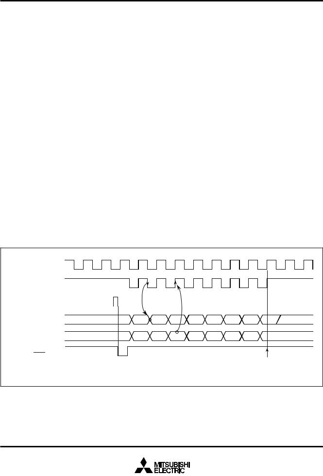
MITSUBISHI MICROCOMPUTERS
M37207MF-XXXSP/FP, M37207M8-XXXSP
M37207EFSP/FP
SINGLE-CHIP 8-BIT CMOS MICROCOMPUTER for VOLTAGE SYNTHESIZER and ON-SCREEN DISPLAY CONTROLLER
____ |
Notes 1: On programming, note that the serial I/O counter is set by |
Internal clock : The SRDY signal goes to HIGH during the write cycle |
|
by writing data into the serial I/O register (address 00DD16). After the |
writing to the serial I/O register with the bit managing in- |
____ |
structions such as SEB and CLB. |
write cycle, the SRDY signal goes to “L” (receive enable state). The |
|
____ |
2: When an external clock is used as the synchronous clock, |
SRDY signal goes to “H” at the next falling edge of the transfer clock |
|
for the serial I/O register. |
write transmit data to the serial I/O register when the trans- |
The serial I/O counter is set to “7” during write cycle into the serial I/ |
fer clock input level is HIGH. |
O register (address 00DD16), and transfer clock goes HIGH forcibly. |
|
At each falling edge of the transfer clock after the write cycle, serial |
|
data is output from the SOUT pin. Transfer direction can be selected |
|
by bit 5 of the serial I/O mode register. At each rising edge of the |
|
transfer clock, data is input from the SIN pin and data in the serial I/O |
|
register is shifted 1 bit. |
|
After the transfer clock has counted 8 times, the serial I/O counter |
|
becomes “0” and the transfer clock stops at HIGH. At this time the |
|
interrupt request bit is set to “1.” |
|
External clock : When an external clock is selected as the clock source, |
|
the interrupt request is set to “1” after the transfer clock has counted |
|
8 counts. However, transfer operation does not stop, so the clock |
|
should be controlled externally. Use the external clock of 1 MHz or |
|
less with a duty cycle of 50%. |
|
The serial I/O timing is shown in Figure 19. When using an external |
|
clock for transfer, the external clock must be held at “H” for initializing |
|
the serial I/O counter. When switching between an internal clock and |
|
an external clock, do not switch during transfer. Also, be sure to ini- |
|
tialize the serial I/O counter after switching. |
|
Synchronous clock
Transfer clock
Serial I/O register
write signal 
 (See note)
Serial I/O output |
D0 |
D1 |
D2 |
D3 |
D4 |
D5 |
D6 |
D7 |
|
SOUT |
|||||||||
|
|
|
|
|
|
|
|
Serial I/O input
SIN
Receive enable signal SRDY
Interrupt request bit is set to “1”
Note : When an internal clock is selected, the S OUT pin is at high-impedance after transfer is completed.
Fig. 19. Serial I/O Timing (for LSB first)
26
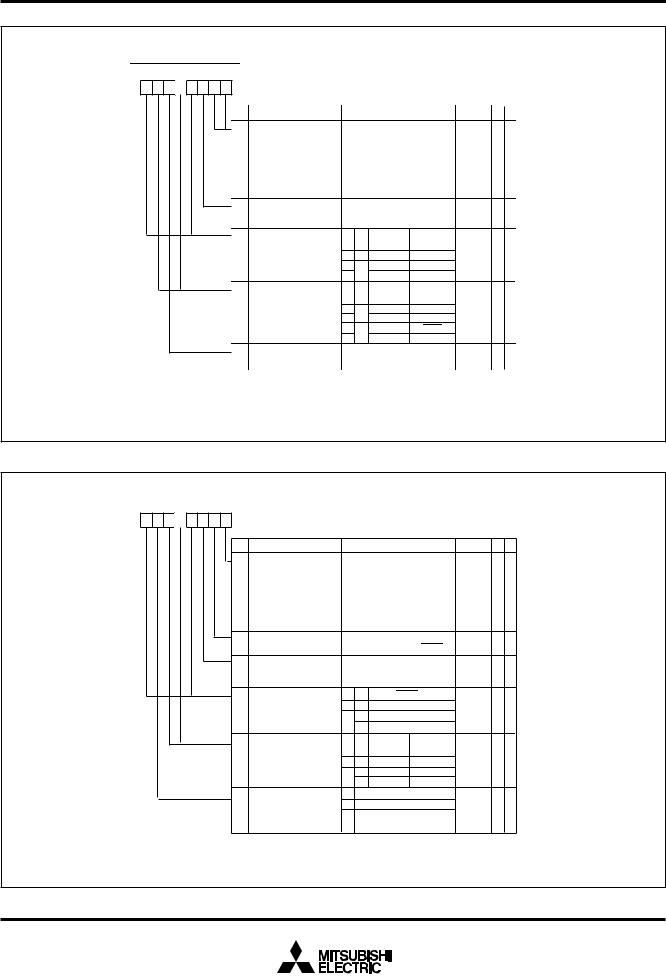
MITSUBISHI MICROCOMPUTERS
M37207MF-XXXSP/FP, M37207M8-XXXSP
M37207EFSP/FP
SINGLE-CHIP 8-BIT CMOS MICROCOMPUTER for VOLTAGE SYNTHESIZER and ON-SCREEN DISPLAY CONTROLLER
Serial I/O Mode Register
b7b6 b5 b4 b3 b2 b1 b0
Serial I/O mode register (SM) [Address 00DE16]
B |
Name |
|
|
Functions |
|
After reset R W |
|
0, 1 Internal synchronous |
b1 b0 |
|
|
0 |
R W |
||
|
clock selection bits |
0 0: f(XIN)/4 or f(XCIN)/4 |
|
|
|||
|
(SM0, SM1) |
0 1: f(XIN)/16 or f(XCIN)/16 |
|
|
|||
|
(See note 1) |
1 0: f(XIN)/32 or f(XCIN)/32 |
|
|
|||
|
|
1 1: f(XIN)/64 or f(XCIN)/64 |
|
|
|||
2 |
Synchronous clock |
0: External clock |
|
0 |
R W |
||
|
selection bit (SM2) |
1: Internal clock |
|
|
|
||
3, 7 Ports P40, P41 |
b7 b3 P40/SOUT2/ |
P41/SCLK2/ |
0 |
R W |
|||
|
function selection |
|
0 |
SDA3/XCIN SCL3/XCOUT |
|
|
|
|
bits (SM3, SM7) |
|
P40 |
P41 |
|
|
|
|
(See note 2) |
0 |
1 |
SOUT2 |
SCLK2 |
|
|
|
|
1 |
|
SDA3 |
SCL3 |
|
|
4, 6 Ports P42, P43 |
b6 b4 |
P42/SIN2/ |
P43/SRDY2/ |
0 |
R W |
||
|
function selection bits |
0 |
0 |
SDA2/AD8 |
SCL2/AD7 |
|
|
|
(SM4, SM6) |
P42 |
P43 |
|
|
||
|
(See note 2) |
1 |
1 |
SDA2 |
|
|
|
|
|
0 |
P42 |
SRDY2 |
|
|
|
|
|
1 |
|
SDA2 |
SDA2 |
|
|
5 |
Transfer direction |
0: LSB first |
|
0 |
R W |
||
|
selection bit (SM5) |
1: MSB first |
|
|
|
||
|
|
|
|
|
|
|
|
Notes 1: Either f(XIN) or f(XCIN) is selected by bit 7 of the CPU mode register.
2:When using ports P4 0–P43 as serial I/O pins, set bit 1 of the serial control register to “1.”
Fig. 20. Serial I/O Mode Register
Serial I/O Control Register
b7b6 b5 b4 b3 b2 b1 b0
Serial I/O control register (SIC) [Address 020716]
B |
Name |
|
Functions |
0 Input signal to sift |
CSIO b0 |
||
|
register selection bit |
0 |
0: Input signal from S IN1 |
|
(SIC0) |
0 |
1: Input signal from S OUT1 |
|
|
|
(See note 1) |
|
|
1 |
0: Input signal from S IN2 |
|
|
1 |
1: Input signal from S OUT2 |
|
|
|
(See note 1) |
After reset R W
0 R W
1Serial I/O pin switch bit (CSIO)
2I2C-BUS connection ports switch bit (SIC2)
3, 7 Ports P47 function selection bits (SM3, SM7)
(See note 2)
0: SOUT1,SCLK1, SIN1, SRDY1 |
0 |
R W |
||
1: SOUT2,SCLK2, SIN2, SRDY2 |
|
|
||
0: SDA2, SCL2, SDA1, SCL1 |
0 |
R W |
||
1: SDA3, SCL3 |
|
|
||
b7 b3 |
P47/SRDY1/PWM8 |
0 |
R W |
|
0 |
|
P47 |
|
|
1 |
0 |
SRDY1 |
|
|
|
1 |
PWM8 |
|
|
4, 5 Ports P44, P45 |
b5 b4 P44/SOUT1/ |
P45/SCLK1/ |
0 |
R W |
||
function selection bits |
0 |
|
SDA1 |
SCL1 |
|
|
(SM4, SM6) |
|
P44 |
P45 |
|
|
|
(See note 2) |
1 |
0 |
SOUT1 |
SCLK1 |
|
|
|
|
1 |
SDA1 |
SCL1 |
|
|
6 Ports P46 function |
b6 |
|
P46/SIN1/PWM9 |
0 |
R W |
|
selection bits |
0 |
|
P46 |
|
|
|
(SIC6) |
1 |
|
PWM9 |
|
|
|
(See note 2) |
|
|
|
|
|
|
Notes 1: When inputting data from the S out pin, set “FF16” to the serial
I/O register.
2:When using ports P4 4–P47 as serial I/O pins, set bit 1 of the serial I/O control register to “0.”
Fig. 21. Serial I/O Control Register
27
MITSUBISHI MICROCOMPUTERS
M37207MF-XXXSP/FP, M37207M8-XXXSP
M37207EFSP/FP
SINGLE-CHIP 8-BIT CMOS MICROCOMPUTER for VOLTAGE SYNTHESIZER and ON-SCREEN DISPLAY CONTROLLER
Serial I/O Common Transmission/Reception Mode
By writing “1” to bit 0 of the serial I/O control register, signals SIN and SOUT are switched internally to be able to transmit or receive the serial data.
Figure 22 shows signals on serial I/O common transmission/reception mode.
Note : When receiving the serial data after writing “FF16” to the serial
I/O register.
“1”
SCLK2
“0” CSIO
SOUT2 

 “1”
“1”
“0”
SIN2 |
“1” |
“0” SCLK1  CSIO
CSIO
SOUT1

 Clock
Clock
“1”

 Serial I/O shift register (8)
“0”
SIC0
SIC0 : Bit 0 of serialI/O control register CSIO : Bit 1 of serial I/O control register
SIN1
Fig. 22. Signals on Serial I/O Common Transmission/Reception Mode
28
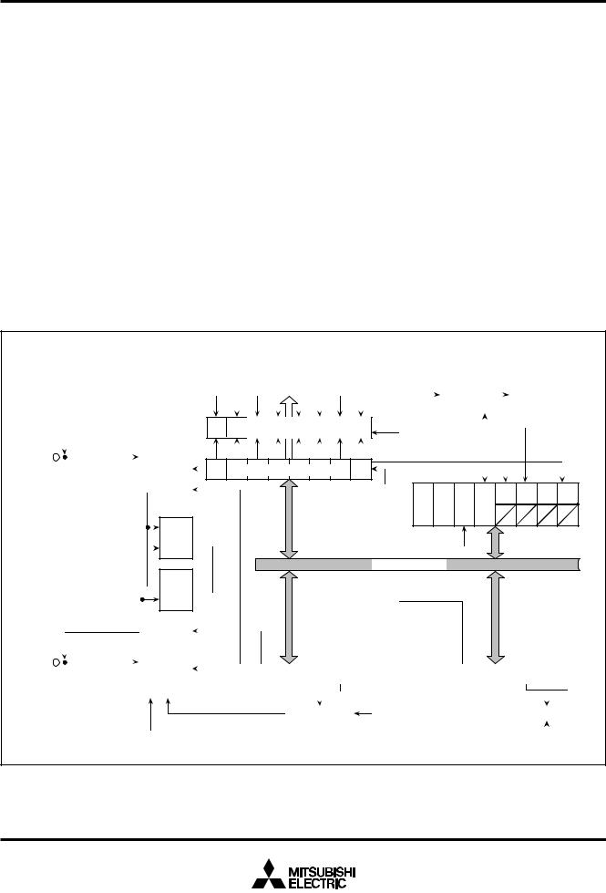
MITSUBISHI MICROCOMPUTERS
M37207MF-XXXSP/FP, M37207M8-XXXSP M37207EFSP/FP
SINGLE-CHIP 8-BIT CMOS MICROCOMPUTER for VOLTAGE SYNTHESIZER and ON-SCREEN DISPLAY CONTROLLER
MULTI-MASTER I2C-BUS INTERFACE
The multi-master I2C-BUS interface is a serial communications circuit, conforming to the Philips I2C-BUS data transfer format. This interface, offering both arbitration lost detection and a synchronous functions, is useful for the multi-master serial communications.
Figure 23 shows a block diagram of the multi-master I2C-BUS interface and Table 2 shows multi-master I2C-BUS interface functions. This multi-master I2C-BUS interface consists of the I2C address register, the I2C data shift register, the I2C clock control register, the I2C control register, the I2C status register and other control circuits.
Table 2. Multi-master I2C-BUS Interface Functions
Item |
Function |
|
|
In conformity with Philips I2C-BUS |
|
|
standard: |
|
Format |
10-bit addressing format |
|
7-bit addressing format |
||
|
||
|
High-speed clock mode |
|
|
Standard clock mode |
|
|
In conformity with Philips I2C-BUS |
|
|
standard: |
|
Communication mode |
Master transmission |
|
Master reception |
||
|
||
|
Slave transmission |
|
|
Slave reception |
|
SCL clock frequency |
16.1 kHz to 400 kHz (at f = 4 MHz) |
f : System clock = f(XIN)/2
Note: We are not responsible for any third party’s infringement of patent rights or other rights attributable to the use of the control function (bits 6 and 7 of the I2C control register at address 00F916) for connections between the I2C-BUS interface and ports (SCL1, SCL2, SDA1, SDA2).
b7 I2C address register (S0D) b0
Serial |
|
|
|
Noise |
|
Data |
|
data |
elimination |
|
control |
(SDA) |
circuit |
|
circuit |
|
|
|
|
AL circuit
SAD6 |
SAD5 |
SAD4 |
SAD3 |
SAD2 |
SAD1 |
SAD0 |
RBW |
|
Interrupt |
Interrupt |
|
|
|
|
|
|
|
|
|
generating |
request signal |
|
|
|
|
|
|
|
|
|||
|
|
|
|
|
|
|
|
|
circuit |
(IICIRQ) |
|
|
|
|
|
|
|
|
|
|
|
|
Address comparator |
|
|
b7 |
b0 |
|
|
|
I2C data shift register |
|
|
S0 |
b7 |
|
b0 |
|
|
AL AAS AD0 LRB |
|
|
|
|
|
|
MST TRX |
BB |
PIN |
|
|
|
I2 C status |
|
|
|
register (S1) |
|
Internal data bus |
|
|
 BB circuit
|
|
|
|
|
|
|
|
|
|
|
|
|
|
|
|
|
|
|
|
|
|
|
|
Serial |
Noise |
|
Clock |
|
b7 |
|
|
|
|
|
|
|
|
b0 |
|
b7 |
|
|
|
|
|
|
b0 |
clock |
elimination |
|
control |
|
|
|
|
|
|
|
|
|
|
|
|
|
|
|
|
||||
(SCL) |
circuit |
|
circuit |
|
ACK |
ACK |
FAST |
CCR4 |
CCR3 |
CCR2 |
CCR1 |
CCR0 |
|
BSEL1 |
BSEL0 |
10BIT |
ALS |
ESO |
BC2 |
BC1 |
BC0 |
||
|
|
|
BIT |
MODE |
|
SAD |
|||||||||||||||||
|
|
|
|
|
|
|
|
|
|
|
|
|
|
|
|
||||||||
|
|
|
|
I2C clock control register (S2) |
|
|
|
I2C clock control register (S1D) |
|||||||||||||||
|
|
|
|
|
|
|
|||||||||||||||||
|
|
|
|
|
|
|
|
|
|
Clock division |
|
|
System clock (φ) |
|
|
|
Bit counter |
||||||
Fig. 23. Block Diagram of Multi-master I2C-BUS Interface
29
MITSUBISHI MICROCOMPUTERS
M37207MF-XXXSP/FP, M37207M8-XXXSP M37207EFSP/FP
SINGLE-CHIP 8-BIT CMOS MICROCOMPUTER for VOLTAGE SYNTHESIZER and ON-SCREEN DISPLAY CONTROLLER
(1) I2C Data Shift Register
The I2C data shift register (S0 : address 00D916) is an 8-bit shift register to store receive data and write transmit data.
When transmit data is written into this register, it is transferred to the outside from bit 7 in synchronization with the SCL clock, and each time one-bit data is output, the data of this register are shifted one bit to the left. When data is received, it is input to this register from bit 0 in synchronization with the SCL clock, and each time one-bit data is input, the data of this register are shifted one bit to the left.
The I2C data shift register is in a write enable status only when the ESO bit of the I2C control register (address 00DC16) is “1.” The bit counter is reset by a write instruction to the I2C data shift register. When both the ESO bit and the MST bit of the I2C status register (address 00F816) are “1,” the SCL is output by a write instruction to the I2C data shift register. Reading data from the I2C data shift register is always enabled regardless of the ESO bit value.
Note: To write data into the I2C data shift register after setting the MST bit to “0” (slave mode), keep an interval of 8 machine cycles or more.
(2) I2C Address Register
The I2C address register (address 00DA16) consists of a 7-bit slave
___
address and a read/write bit. In the addressing mode, the slave address written in this register is compared with the address data to be
received immediately after the START condition are detected.
____
■Bit 0: Read/Write Bit (RBW)
Not used when comparing addresses, in the 7-bit addressing mode.
In the 10-bit addressing mode, the first address data to be received is compared with the contents (SAD6 to SAD0 + RBW) of the I2C address register.
The RBW bit is cleared to “0” automatically when the stop condition is detected.
■Bits 1 to 7: Slave Address (SAD0–SAD6)
These bits store slave addresses. Regardless of the 7-bit addressing mode and the 10-bit addressing mode, the address data transmitted from the master is compared with the contents of these bits.
I2C Data Shift Register
b7 b6 b5 b4 b3 b2 b1 b0
I2C data shift register1(S0) [Address 00D916]
B |
Name |
Functions |
After reset |
R |
W |
0 |
D0 to D7 |
This is an 8-bit shift register to store |
Indeterminate |
R |
W |
to |
|
receive data and write transmit data. |
|
|
|
7 |
|
|
|
|
|
Note: To write data into the I2C data shift register after setting the MST bit to “0” (slave mode), keep an interval of 8 machine cycles or more.
Fig. 24. I2C Data Shift Register
I2C Address Register
b7 b6 b5 b4 b3 b2 b1 b0
I2C address register (S0D) [Address 00DA16]
B Name
0Read/write bit (RBW)
1Slave address
to (SAD0 to SAD6) 7
Functions |
After reset R W |
|
0: Read |
0 |
R — |
1: Write |
|
|
The address data transmitted from |
0 |
R W |
the master is compared with the |
|
|
contents of these bits. |
|
|
Fig. 25. I2C Address Register
30
Loading...