


TRAINING BOOK
FOR DIGITAL AMPLIFIER RECEIVER RX-D… SERIES
By JSCA ENGINEERING DEPARTMENT |
JUNE 2006 |
Second Edit |
November 2006 |

CONTENT
•OVERALL
•POWER SUPPLY
•POWER PROTECTION
•DIGITAL AMPLIFIER
•AUDIO DIGITAL PROCESS
•VIDEO DIGITAL PROCESS & HDMI *
•USB WIRE OR WIRELESS**
*THESE FEATURES APPLY TO RX-D401//402/701/702 ONLY.
** WIRELESS APPLIES TO RX-D301/302/701/702 ONLY.

OVERALL BLOCK DIAGRAM
Signal Flow and DC Power Supply
* |
|
IN |
|
DVD A. Multi
=DIGITAL SIGNAL |
|
|
|
|
|
|
|
|
|
|
|
|
|
|
|
|
|
|
|
|
|
|
|
=ANALOG SIGNAL |
|
||||
OVERALL BLOCK DIAGRAM note
•A AUDIO means Analog audio, D-OUT means Digital audio output.
•The HDMI outputs video only, even when the HDMI input has both video & audio data. In the future models, the HDMI will output both A
&V data.
•The digital audio output is not available on models RX-D201/202. The output format is the same as the digital input signal; other audio input signals (including HDMI & USB) cannot go through the DIGITAL OUT.
•The front left & right speaker out audio is applied to headphones. The CPU will turn off the 7 speaker relays after it detects the headphone jack is plugged in.
•The ‘DVD analog multi channel’ input audio bypassesthe DSP board, and goes into Master Volume Board directly.
•directly.

POWER SUPPLY BLOCK DIAGRAM
‘AMP_+/-B’ switch regulator

POWER SUPPLY 1/5
Regulate
PCB
Master Clock PCB
IC201/301 |
IC401/801 |
PWM PCB |
CN530-5
 Q171
Q171
CN114-4
R152 +12V_RY CN530-7
CN114-3
D+5V_DSP
POWER SUPPLY 1/5 note
•The power supply circuits for 2005 year of RX-D… ser ies are similar. One main difference is the ‘D+5V_HDMI’ is not in models RX-D201/202/301/302.
•There are two AC power transformers in the unit.
1.T101 for standby power: supplies D+5V and B+5V_Mi DC power for CPU IC501 and RY+9V (power ON/OFF relay circuit).
2.T102 for unit operation after power on: There are more than 15 different DC voltages provided for unit operation after power is turned on.
•The DC voltages: +B, AMP+B, AMP-B+12V and DCDC_-B+12V all vary (along with output volume) referenced to ground. The ‘–B’ v oltage is -50v~ -62v referenced to ground. The label ‘DCDC_-B+12V’ DC voltage means this is the DC voltage supply to the DCDC converter circuit, the +12 DC refers to –B; if referenced to ground, it is -38v~-50v.
•The +B and AMP+B voltages are higher in models RX-D402/702, because the output power is higher than RX-D201/202.
•The +2.5v, DCDC_+12V, DCDC_-B+12V, AMP-B+12V, D+5V_DSP and D+5V_HDMI are not produced in the main PCB.
•You could check all of the voltages at the indicated (underlined) locations without any extension cable, before or after power is turned on. (See the next page)
•Some additional DC voltages are produced in ‘Regulate PCB’ and ‘Master clock PCB’.

POWER SUPPLY 2/5
(CN130)
CN114
3. D+5V_DSP
4. D+5V_HDMI *
* The ’D+5V_HDMI’ for models RX-D401/402/702 only.
The ‘AMP_+/-B’ switch regulator POWER SUPPLY 3/5 composes three sections:
1.MOSFET switch circuit (the important parts are Q1101/1102, D1107/1108, L1101/1102, C1117/1118…)
2.Switch driver circuit-IC101.
3.DC-DC Converter Control Board
3 |
2 |
1 |
|
|
DC-DC |
MOSFET |
+ |
||
MOSFET |
|
|||
CONVERTER |
DRIVE |
|
||
AMP_B |
||||
CONTROL |
IC101 |
SWITCH |
|
|
|
||||
Q1101/1102… _ |
||||
|
|
|||
AMP_ +/-B |
SOUND |
7 CHANNEL |
|
LEVEL |
|||
LEVEL |
POWER |
||
CONTROL |
|||
DETECT |
AMP |
||
CPU IC501 |
|||
|
|
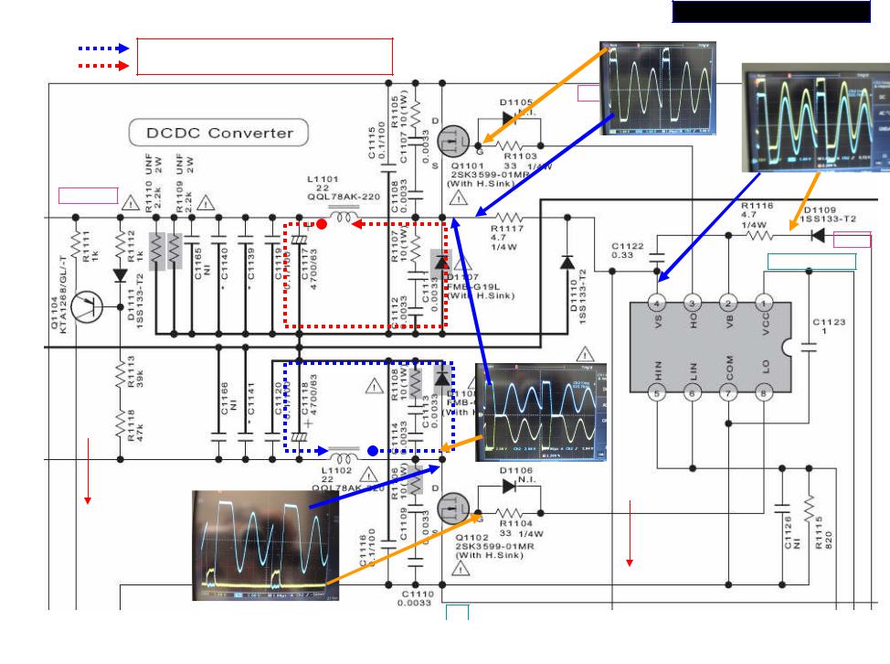
‘AMP_ +/-B’ switch regulator-1a
The CEMF current (via D1107/8) loop after Q1101/1102 switch off.
+B
AMP_+B
|
V. feedback |
|
|
|
|
|
|
|
det. |
|
AMP_-B |
|
V.out |
|
|
|
|
||
|
|
|
|
|
POWER SUPPLY 3/5
+12V
-B +12V
-B
POWER SUPPLY 3/5
Tip to measure the outputs of Q1101/1102

POWER SUPPLY 3/5
Waveform (1) at ‘AMP_+/-B’ switch regulator
There is 10v At |
|
|
|
|
|
|
|
Yellow at G of Q1101 –channel 2 |
|
|
|||
Gate higher than |
|
|
|
|
|
|
|
|
|
|
Blue at S of Q1101channel 1 |
||
|
|
+B |
|
|
||
Source for |
|
|
|
|
||
|
||||||
switches Q1101 |
|
|
(+60V.) |
|
||
on. |
|
|
|
|
|
|
|
|
|
|
|
|
|
AMP+B (+30V.)
1 |
3 |
Q1101 on |
|
0 V. |
Damped oscillation |
|
|
2 |
D1107 on |
The waveforms at Source and Gate of Q1101. Three periods in one cycle of oscillation: 1.Q1101 turned on; 2. D1107 turned on by CEMF; 3. Damped LC oscillation; Q1101 is switched off during period 2 and 3.

POWER SUPPLY 3/5
Waveform (2) at ‘AMP_+/-B’ switch regulator
About 10v pulse at Gate of Q1102 when switch on
|
|
|
Both channels are DC coupling |
|
|
DC 0v line |
|
||
|
|
|
|
|
|
|
|
|
|
|
|
|
|
|
Blue at D of Q1102channel 2 |
|
|||
|
|
|
|
|
AMP -B
About
-30v
Yellow at G of Q1102
-B
Both channel X 10
About
-63v
The waveforms at gate and drain of Q1102 after power is turned on.

POWER SUPPLY 3/5
KNOW THE MOSFET
2SK3599-01MR and IRFB4212 are Enhancement-type N-channel MOSFET
|
+ |
• Enhancement-type MOSFET is also known as |
|
|
|
|
|
normally off (when VGS=O, Drain current=o) MOSFET. |
+ |
|
• N-channel MOSFET: The more positive the gate |
|
voltage (VGS), the greater the drain current. |
|
|
|
-
• There is a built in zener diode in these two kinds of MOSFET, but it does not show in manual’s diagram.
• The RDS (resistance between Drain and Source) will increase when VGS drop to below 8v; and it causes the MOSFET to get very hot and damage.
• MOSFETs have a thin layer of silicon dioxide; this insulating layer is kept as thin as possible to give the gate more control over drain current. Because the insulating layer is so thin, it is easily destroyed by excessive gate-source voltage.
• The transient voltages by inductive kickback and other effects may exceed the VGS (max) rating; even handling a MOSFET may deposit enough static charge to exceed the
VGS (max) rating.

POWER SUPPLY 3/5
•If the positive drive pulse at Gate is less than 8 volts (refer to Source), the MOSFET will get very hot to damage. If the drive pulse is not sharp or is very noise, it makes MOSFET very hot also.
•If the drive pulse is low & noisy, the drive IC or peripheral parts may be defective or the power supply may not be functioning properly.
•When handling the MOSFET, try not to touch the pins with your fingers.
•It is preferable to use anti-static iron when soldering the MOSFET.
•When the pair of MOSFETs are damaged, sometimes the drive IC becomes defective too. Check the drive circuit before replacing the MOSFETs, to prevent the power MOSFET from shorting again.

POWER SUPPLY 3/5
‘AMP_ +/-B’ switch regulator-1b
CEMF charge path
+B 70 V
ANP+B 30V |
+ |
_ |
(+30 V) * |
|
|||
|
|
|
In this circuit it, seems no current through D1107, but D1107 is high power Schottky Diode with heat sink, If You mean with DC Volt meter but if you use Oscilloscope you can see the
negative peak is clipped. This clipping is by D1107 WHY? *DC METER CHECK
Because there is a large charge current through D1107 that forced by CEMF.

POWER SUPPLY 3/5
What is CEMF?
In the relay driver circuit, always has a diode parallel with coil, WHY?
Counter-Electromotive Force (CEMF) is a voltage developed in an inductor network by a pulsating current or an alternating current. The voltage's polarity is at every moment reverse that of the input voltage, therefore opposes the change of main current flow in the circuit it is called counter-electromotive force (CEMF). The CEMF is then given by:
(the ‘–’ sign means polarity reverse)
Where i is the current, T is time and L is the inductance (L1101) of the circuit. When the ‘dt’ is very and very small the CEMF (voltage) will become extremely high.
If diode (D1107) is defected it can cause damage to peripheral components

POWER SUPPLY 3/5
‘AMP_ +/-B’ switch regulator-2
IC101- Drive IC for Q1101/1102
DCDC +12V
VERAG
DC 42v
2
C1122 |
+B |
5 |
3 |
AMP+B
4
-B_+12V
AMP-B
1
6
8 |
-B |
|
7 -B
Audio
PWM  CPU
CPU  Level
Level
detector

Bootstrap Voltage USE THE DC CLAMPER
Bootstrap Voltage The additional higher positive voltage added to the low DC voltage
Averag e
+30v
INPUT
AVERAGE
DC 30V
1. Capacitor coupling block out the input DC level.
OUTPUT
AVERAGE DC
Averag
e
+0v 0V
2. The DC clamper recovers the DC level at output. *
Averag e
+30v
29.3V
*In fact it is about +29.3v due to diode forward bias drop.
3.The DC clamper adds DC level to the output.
|
Averag |
|
|
e |
42V |
|
+42v |
|
|
|
|
+ |
|
|
12v |
12v |
|
- |
|
|
|
|

POWER SUPPLY 3/5
•IC101 is high power MOSFET drive with independent high and low side reference output channels.
•The power supply for the high channel drive is floated.
•The bootstrap voltage from VS to VB through 0.33uF capacitor C1122.
•This causes DC level at pin2-VB to be always approximately 11v higher than pin 4-VS.
•The UV (under voltage) detector is built in the IC, if the power supply voltage drops below the threshold level (about 7.5-8.3 v), The IC stops output.
•If IC101 was shorted, sometimes peripheral resistors are burnt out also.
POWER SUPPLY 3/5
Waveform (3) at ‘AMP_+/-B’ switch regulator
Yellow at pin 2 of IC101 (R1110)
About 11v.
Blue at S of Q1101channel 1
DC 0v line
Always about 11v different between pin 2 and pin4 of IC101.

POWER SUPPLY 3/5
Tip to measure IC101
CN115 P-1
DCDC +12V
CN115 PIN4
–B_+12V
CN115 P-5
--B
CN152 P-4
Vout_DET
CN152 P-11
Vout_DET

‘AMP_ +/-B’ switch regulator-3
POWER SUPPLY 3/5
Q1501-
Buffer
the
And ‘V out’ detector

POWER SUPPLY 3/5
|
CPU IC501 |
|
|
|
PIN 62 |
PIN 65 |
|
|
|
|
|
CN151 |
PIN 7 |
PIN 8 |
AMP +/- B |
|
H |
H |
25V |
|
|
|
|
|
L |
H |
35V |
|
|
|
|
|
L |
L |
42V |
|
|
|
|
•The AMP + B voltages vary from about +25v to +42v; depending on the power output of 7 channels at final stage before speaker terminal (The voltages are higher in models RX-D401/402/702)
•When the audio output level (the analog negative feedback [A NFB] that comes from the audio final output) is increasing, the DC level at the cathode of diodes D211-D311…
(7 diodes) is increased proportionally.
•This increased DC voltage via buffer Q1501 turns on Q541 first (0.7v), and will turn on both Q541 and Q542 if the DC level rises higher (2.57v). Then the low state will input to pins 66 and 90 of IC501 (OUT_LEVEL 1 and OUT_LEVEL 2). This causes IC501 to output a low state on pins 62 and 65 (V CHANGE_1 and V CHANGE_2) to DCDC CONVERTOR CONTROL board.
•These low state inputs (through CN151 pin 7 & 8) switch off Q1151, Q1152, and it effects the DC level at pin 1 of IC111 (error amp). Finally, it changes the PWM pulse’s duty cycle duration at IC112 pin 1, thus rises the AMP + B voltage to around + 35v ( VCHANG_1 active only) or + 42v (both VCHANGE_ 1 and _2 are active).
•The ‘FEEDBACK‘ from ‘AMP+B’ goes into ERROR AMP IC111 pin 3 through CN151 pin 2, it is for stabilizing the ‘AMP+B’ regulation.

POWER SUPPLY 4/5
+2.5V regulator built-in the IC supply to digital circuit inside and outside of IC.
+7V
+2.5V
-2.5V
-7V
Use of the built-in ±2.5V regulated supply to the inside and outside digital circuits, especially for master clock generation circuit, prevents digital noise interference to analog GND.

POWER SUPPLY 5/5
Some Other DC Voltages Not In Main PCB
DC +3.3V, +1.8V, +1.2V and TX5V
HDMI BOARD |
1 IN 5V IC791 |
5 |
DSP BOARD |
|
|
|||
|
OUT 3.3 V |
|
|
|
|
7 IN 5V |
|
|
|
2 ADJ---------- 1.8V |
4 |
|
|
|
|
IC692 |
|
1 IN 9V |
|
|
|
|
|
|
|
|
|
|
1 |
IN 5V |
IC691 |
|
OUT 3.3V 1 |
|
|
IC793 |
1 IN 5V IC792 |
|
|
|
||||
|
|
|
OUT 3.3 V |
5 |
|
|
||
|
OUT 3.3 V |
5 |
|
|
|
|
||
OUT TX5V 5 |
2 ADJ---------- 1.2V |
4 |
|
|
||||
2 ADJ---------- 1.8V |
4 |
APPLY IN |
|
|||||
|
|
|
|
|
|
|||
|
|
|
|
|
|
|
BOARD |
3 |
|
|
|
|
|
C661 |
|
CN662- |
|
|
|
|
|
|
|
|
||
OUT PIN 18 |
|
|
|
|
DSP |
CN661-3 |
|
|
|
|
|
|
|
|
|
|
|
USB BOARD IN -3.3V 3
CN11
wireless
FRONT INPUT IN-
BOARD 3.3V
CN961 3
POWER SUPPLY 5/5 NOTE
•IC791, IC792 and IC691 are same type of regulator IC and the voltage from ‘output 2’ (pin4 of the IC) can be adjusted. We see the voltage is 1.2v at pin 4 of IC691, and others are 1.8v.
•IC793 outputs TX5V to the HDMI out jack, this 5v is sent to the outside video monitor for HDMI connection detect; without this 5v, the monitor cannot accept signals from the HDMI input.
•The +2.5v and -2.5v also are not produced in main PCB, they are from the PWM PCB; shown on the previous page.

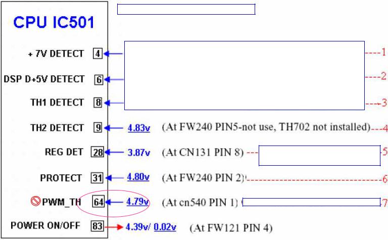
PROTECTION CICUIT 1/8
FOR MODELS: RX-D201/202/301/302
Where to measure
7 protect inputs
Not use (Q212/213 R226 NI)
PROTECTION CICUIT 1/8 NOTE
•If the power auto shuts off a few seconds after turn on, most likely it is caused by the power protection circuit. We describe the protection circuit on models RX-D201/202. It is similar to other RX-D… series models and can be used as a reference for troubleshooting.
•There are 7 protection input pins (only 5 pins used in these 4 models) on CPU IC501; any of them could cause the protection circuit to be triggered and shut down the power. The marked voltages are +5~10% tolerance.
•The underline marked voltages can be measured in power standby mode; (e.g. 2.01v, 4.83v …) but have to be checked again once power is on.
PROTECTION CICUIT-SUP. 1
For models RX-D401/402/701/702
These 3 pins are NOT usedprotectfor
inputs
protection input on models
RX-D401/402/701/702
THERMAL |
|
|
|
4 |
|
For models RX-D401/203/701/702 |
|
2.01v |
|
|
|||
|
|
|
|
|
|
|
Include +7v, DSP D+5V,
D+5V_HDMI DETECTION.
Not use, because Q212,213 and R220 are NI.
 Loading...