Page 1

Research & Development
SPI-Interface
Specifications
for SPOT
CDS500D & CDS550D
OEM
Capacitance Diaphragm
Sensors
V 1.1
November 10, 2014
SPOT CDS500D & CDS550D OEM Sensor SPI-Interface Specification_V1.1 Page 1 of 14
Christian Berg, T based on Felix Mullis, TL Created 11/10/2014 2:36:00 PM
Page 2

Research & Development
1 Table of Contents
1 Table of Contents ............................................................................................................. 2
2 Hardware Concept ............................................................................................................ 3
2.1 Hardware Block Diagram ............................................................................................................... 3
2.2 Interface Connector and Cable ...................................................................................................... 4
2.3 Grounding Concept ........................................................................................................................ 4
2.4 Timing Specifications ..................................................................................................................... 4
2.5 Interface Hardware Specifications ................................................................................................. 5
2.5.1 Power Supply .......................................................................................................................... 5
2.5.2 Recommended operating conditions....................................................................................... 5
2.5.3 SPI Interface ............................................................................................................................ 6
3 Read Results ..................................................................................................................... 7
3.1 Pressure ......................................................................................................................................... 7
3.2 Temperature .................................................................................................................................. 8
3.3 Status and Error ............................................................................................................................. 9
3.4 Power-up reset ............................................................................................................................... 9
4 History ............................................................................................................................... 9
5 Appendix ..........................................................................................................................10
5.1 Grounding Concepts .................................................................................................................... 10
5.2 SPI Timing ................................................................................................................................... 11
5.2.1 Introduction ............................................................................................................................ 11
5.2.2 Timing .................................................................................................................................... 11
5.2.3 Total Measurement Cycle ..................................................................................................... 12
5.2.4 Ready-signal ......................................................................................................................... 12
5.2.5 Single Measurement Cycle ................................................................................................... 13
5.2.6 Readout Time Window .......................................................................................................... 13
5.2.7 Conclusion ............................................................................................................................. 14
5.2.8 FAQ’s, Comments ................................................................................................................. 14
SPOT CDS500D & CDS550D OEM Sensor SPI-Interface Specification_V1.1 Page 2 of 14
Christian Berg, T based on Felix Mullis, TL Created 11/10/2014 2:36:00 PM
Page 3

Research & Development
2 Hardware Concept
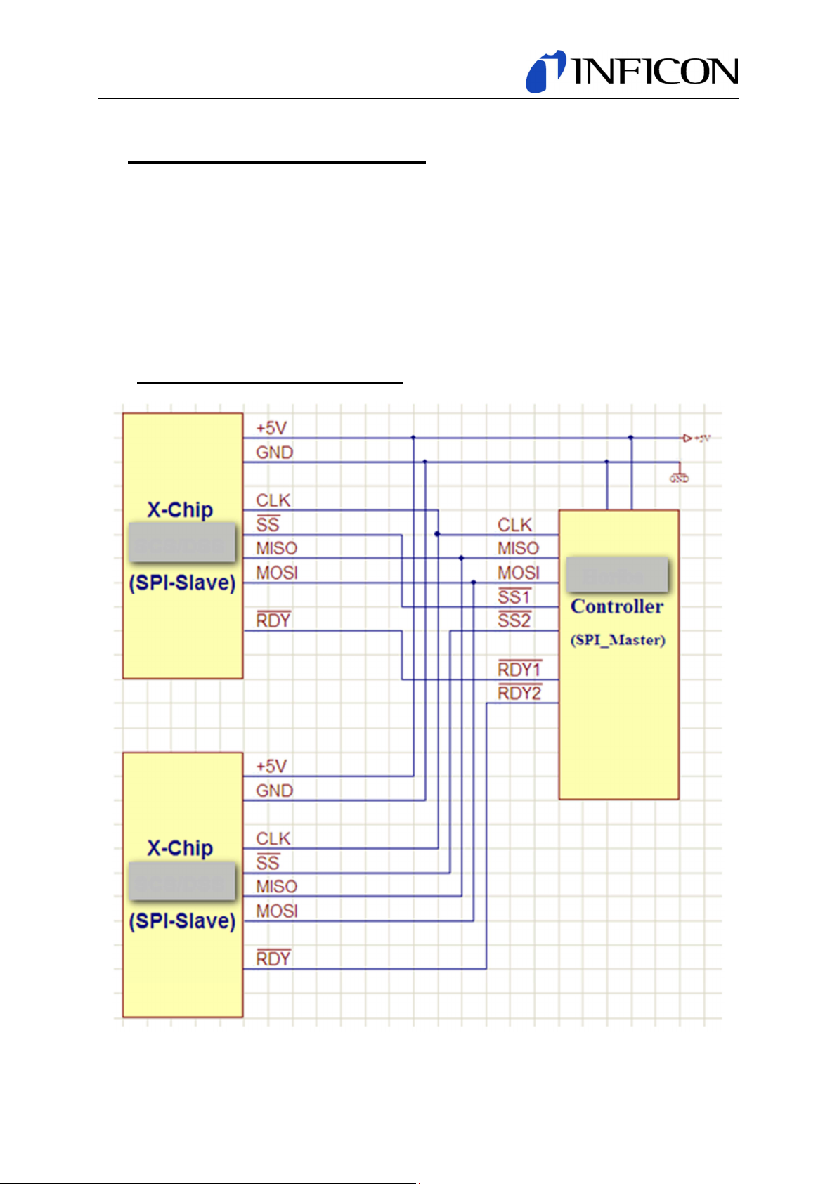
This section describes how two or more SPOT CDS5xxD slaves must be physically connected together with a master. When doing so, the master will be able to receive pressure and temperature data
from each SPOT CDS5xxD slave.
The data exchange link consists of a simple SPI-Interface; therefore only three lines and a chip select
signal are necessary. The additional RDY/ lines signal the end of a measurement cycle. It must be
used in noise critical applications. There it’s forbidden to read data from the chip during measurement
cycles. (Crosstalk from the SPI-interface to the measurement data)
2.1 Hardware Block Diagram
Figure 2.1-1: SPI Block Diagram
SPOT CDS500D & CDS550D OEM Sensor SPI-Interface Specification_V1.1 Page 3 of 14
Christian Berg, T based on Felix Mullis, TL Created 11/10/2014 2:36:00 PM
Page 4

Research & Development
Direction
Signal
Description
MIN TYP MAX
UNIT
2.2 Interface Connector and Cable
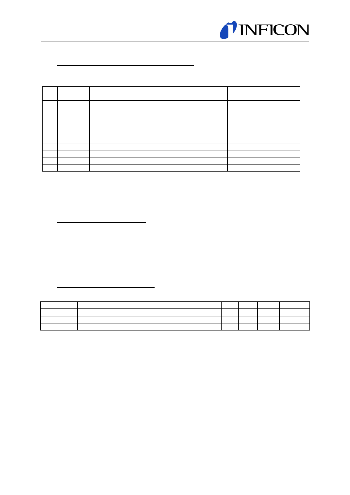
Connector Type: JST 1mm 10 pol.
pin Signal Description
1 +5V Power Supply input
2 GND Supply Common input
3 Clk SPI Clock input
4 SS/ SPI Slave Select (low true) input (low true)
5 MISO SPI Master Input Slave Output output (tristate)
6 MOSI SPI Master Output Slave Input input
7 RDY/ Ready Signal (new measurement value available) output (low true)
8 C1/C0 Internal use only, must be left open output
9 R0/Rref Internal use only, must be left open output
10 Vpp_OTP
Cable length: max. 15 cm
Internal use only, must be left open input
Table 1: pin assignment SPI connector
(SPOT CDS5xxD-side)
2.3 Grounding Concept
The metallic sensor housing (flange) acts as a shielding for the very sensitive electronic measurement
frontend. In order to achieve the specified noise specifications, the sensor flange must be connected
to GND (Supply Common). The impedance of such a connection should be as low as possible. Therefore it is realized directly on the PCB at the frontend of the electronics. This solution guarantees lowest
noise and simultaneously maximizes EMC robustness.
2.4 Timing Specifications
The SPI Timing is described in detail in chapter 5.2 (SPI Timing) in the Appendix.
T_tot_cycle Total Measurement Cycle Time = Data Cycle Time 900 1000 1100 µs
T_sgl_cycle Single Measurement Cycle Time 800 900 1000 µs
T_rd_out Readout Time - - 100 µs
Table 2: SPI Readout Timing
For a description of the above used expressions refer to chapter 5.2 (SPI Timing) in the Appendix.
SPOT CDS500D & CDS550D OEM Sensor SPI-Interface Specification_V1.1 Page 4 of 14
Christian Berg, T based on Felix Mullis, TL Created 11/10/2014 2:36:00 PM
Page 5

Research & Development
Signal
Description
MIN TYP MAX
UNIT
2.5 Interface Hardware Specifications
2.5.1 Power Supply
Vcc Supply voltage 4.75 5.0 5.25 VDC
Ripple Supply voltage ripple and noise (BW = 20MHz) 50 mVpk-pk
Icc Supply current 1 5 mA
2.5.2 Recommended operating conditions
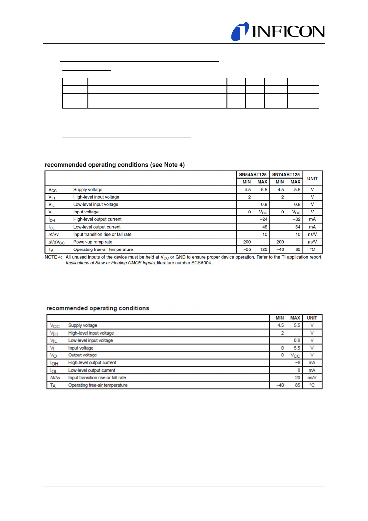
The input lines “Clk”, “SS/” and “MOSI” and the output line “MISO” are buffered with a SN74ABT125.
The output line “RDY/” is driven by a SN74AHCT1G125
SPOT CDS500D & CDS550D OEM Sensor SPI-Interface Specification_V1.1 Page 5 of 14
Christian Berg, T based on Felix Mullis, TL Created 11/10/2014 2:36:00 PM
Page 6

Research & Development
2.5.3 SPI Interface
2.5.3.1 SPI Parameters:
Parameter Description Setting
CPOL Clock Polarity 0, Clock Idle low
CPHA Clock Phase 1, Transmit data on leading edge, read data on falling edge
Mode SPI Mode 1 (CPOL = 0, CPHA = 1)
DORD Bit sequence order 0, MSB first
2.5.3.2 SPI Write
2.5.3.3 SPI Read
2.5.3.4 SPI Timing
Name Symbol Value Unit
Clock frequency fSPI-bus 17 MHz
Clock pulse high-state tpwh 30 ns
Clock pulse low-state tpwl 30 ns
SS/ (SSN) to valid latch tsussn 8 ns
SS/ (SSN) minimal pulse length between write cycles tpwssn 30 ns
Data setup time tsud 6 ns
Data hold time thd 4 ns
Data valid after clock tvd 26 ns
SPOT CDS500D & CDS550D OEM Sensor SPI-Interface Specification_V1.1 Page 6 of 14
Christian Berg, T based on Felix Mullis, TL Created 11/10/2014 2:36:00 PM
Page 7

Research & Development
3 Read Results
The sensor provides 3 values:
• Pressure
• Temperature
• Status
They can be read by a 4 byte SPI-Code as follows:
3.1 Pressure
The SPI communication string for reading the pressure value consists of total 4 bytes as follows:
0x41 – 0x00 – 0x00 – 0x00, only the first byte is relevant, the other three must be sent but the content
of them doesn’t matter.
Read Pressure Op-Code:
Byte_3 Byte_2 Byte_1 Byte_0
0 1 0 0 0 0 0 1
The result (u_press) is a fixed-point number in two’s complement format with a scaling factor of 221 as
follows:
23 22 21 20 19 18 17 16 15 14 13 12 11 10 9 8 7 6 5 4 3 2 1 0
Byte_2 Byte_1 Byte_0
S Integer
The result (u_press) is a fixed-point number in two’s complement format with a scaling factor of 221,
consisting of the sign-bit S, 2 integer and 21 fractional bits. The fourth byte (Byte_3), that’s also received, must be ignored.
The resulting pressure is defined as Full_scale * u_press.
Fractional (21Bits)
p = F.S.R. * u_press
u_press is calculated by dividing the 24-bit result by 2
Examples:
• Fullscale (F.S.R.): 24-bit result = 2’097’152 (0x200000)
• Half F.S.R.: 24-bit result = 1’048’576 (0x100000)
• smallest pos. val: 24-bit result = 1 (0x000001) equals to 0.00000047683 * F.S.R.
• Zero Pressure: 24-bit result = 0 (0x000000)
• smallest neg. val: 24-bit result = -1 (0xFFFFFF) equals to -0.00000047683 * F.S.R.
• neg. Half F.S.R.: 24-bit result = -1’048’576 (0xF00000)
• neg. F.S.R. 24-bit result = -2’097’152 (0xE00000)
21
don’t care
(24 bit read result)
21
. 2
equals 2’097’152.
SPOT CDS500D & CDS550D OEM Sensor SPI-Interface Specification_V1.1 Page 7 of 14
Christian Berg, T based on Felix Mullis, TL Created 11/10/2014 2:36:00 PM
Page 8

Research & Development
3.2 Temperature
The SPI communication string for reading the temperature value consists of total 4 bytes as follows:
0x4D – 0x00 – 0x00 – 0x00, only the first byte is relevant, the other three must be sent but the content
of them doesn’t matter.
Read Temperature Op-Code:
Byte_3 Byte_2 Byte_1 Byte_0
0 1 0 0 1 1 0 1
The result (u_temp) is a fixed-point number in two’s complement format with a scaling factor of 221 as
follows:
23 22 21 20 19 18 17 16 15 14 13 12 11 10 9 8 7 6 5 4 3 2 1 0
Byte_2 Byte_1 Byte_0
S Integer
The result (u_temp) is a fixed-point number in two’s complement format with a scaling factor of 221,
consisting of the sign-bit S, 2 integer and 21 fractional bits. The fourth byte (Byte_3), that’s also received, must be ignored.
The resulting temperature is defined as k * u_temp, where k is defined as a Calibration Constant.
(Typically 25°C).
T = k * u_temp
u_temp is calculated by dividing the 24-bit result by 2
Examples, assuming k = 25°C:
• T ≥ 100°C: 24-bit result = 8’388’607 (0x7FFFFF)
• T = 50°C: 24-bit result = 4’194’304 (0x400000)
• T = 25°C: 24-bit result = 2’097’152 (0x200000)
• T = 0°C: 24-bit result = 0 (0x000000)
• T = -25°C: 24-bit result = -2’097’152 (0xE00000)
(24 bit read result)
Fractional (21Bits)
; k = 25°C
21
don’t’care
21
. 2
equal 2’097’152.
(Calibration Temperature)
SPOT CDS500D & CDS550D OEM Sensor SPI-Interface Specification_V1.1 Page 8 of 14
Christian Berg, T based on Felix Mullis, TL Created 11/10/2014 2:36:00 PM
Page 9

Research & Development
3.3 Status and Error
The SPI communication string for reading the status value consists of total 4 bytes as follows:
0x48 – 0x00 – 0x00 – 0x00, only the first byte is relevant, the other three must be sent but the content
of them doesn’t matter.
Read Status Op-Code:
Byte_3 Byte_2 Byte_1 Byte_0
0 1 0 0 1 0 0 0
Status result:
Byte_3 Byte_2 Byte_1 Byte_0
don’t’ care 24-Bit Status value (Bit 23..0)
Bit
23 SPI communication took place during measurement
13 Pressure error
8 port 3 error
7 port 2 error
6 port 1 error
5 port 0 error
3 Temperature error
All other bits not mentioned here must be ignored.
Description
don’t care
3.4 Power-up reset
After powering up the device, it must be reset by sending the reset command to the device. The reset
command consists of the single byte 0x88h. It is highly recommended to send the reset command
(0x88h) to the sensor after every power up.
4 History
Ver-
Date by Contents
sion
1.0 Jan 17, 2014
1.1 Nov 10, 2014 Felix Mullis timing specification in section 2.4 and 5.2
Christian
Berg
initial version
SPOT CDS500D & CDS550D OEM Sensor SPI-Interface Specification_V1.1 Page 9 of 14
Christian Berg, T based on Felix Mullis, TL Created 11/10/2014 2:36:00 PM
Page 10

Research & Development
5 Appendix
5.1 Grounding Concepts
Situation
• high impedance (> 100kOhm) between sensor elec-
tronics and – housing
• very sensitive measurement frontend (resolution is
fF)
• shielding against noise necessary
• the metallic case of the sensor must be electrically
connected to the power supply reference terminal
(GND) of the driving electronics
Concept #1
• “indirect” connection via earth lines
• easy to implement
• keep impedance of earth connections as low as pos-
sible
Concept #2
• direct connection which may optionally be connected
to earth
• more laborious to implement
• „direct“ connection better shielding possible
SPOT CDS500D & CDS550D OEM Sensor SPI-Interface Specification_V1.1 Page 10 of 14
Christian Berg, T based on Felix Mullis, TL Created 11/10/2014 2:36:00 PM
Page 11

Research & Development
5.2 SPI Timing
5.2.1 Introduction
This chapter describes the principle time-behavior of the SPOT CDS5xxD sensors. This is a generic
timing example. The actual time-behavior is described in section 2.4.Timing Specifications.
5.2.2 Timing
5.2.2.1 Overview
Total measurement cycle
Figure 2 shows the timing overview.
• Ch 1 (yellow) depicts the signal directly at the sensor
• Ch 2 (blue) equals the RDY (Ready) signal
The SPOT CDS5xxD sensor is configured to run “free” meaning that it
1. starts a measurement cycle consisting of 16 single measurements
2. computes the average of this 16 measurements
3. activates the RDY-signal
4. waits until the total measurement cycle time has elapsed
5. jumps back to step 1.
The corresponding timing is explained in more details in the following chapters.
single measurement cycle
Figure 2: Timing Overview
readout time
window
SPOT CDS500D & CDS550D OEM Sensor SPI-Interface Specification_V1.1 Page 11 of 14
Christian Berg, T based on Felix Mullis, TL Created 11/10/2014 2:36:00 PM
Page 12

Research & Development
5.2.3 Total Measurement Cycle
Figure 3: Measurement Cycle
• Ch 1 (yellow) depicts the signal directly at the sensor
• Ch 2 (blue) equals the RDY (Ready) signal
Figure 3 shows a measurement cycle. A measurement cycle is defined as the time between two consecutive negative edges of the Ready-signal. As can be seen from Figure 3, that time equals 682µs.
The timing source for the measurement cycle is an on chip oscillator. Although it is very stable it
shows a relatively large absolute frequency tolerance of about +/- 15% from chip to chip. Therefore the
cycle time can also vary in the range of about +/-15% from sensor to sensor.
5.2.4 Ready-signal
The Ready-signal is active low and it is set after the first measurement value is available. The Readysignal is reset by assigning the SS/-signal active. (SPI Slave Select) that means it is automatically
reset by a consecutive read of the measurement value.
SPOT CDS500D & CDS550D OEM Sensor SPI-Interface Specification_V1.1 Page 12 of 14
Christian Berg, T based on Felix Mullis, TL Created 11/10/2014 2:36:00 PM
Page 13

Research & Development
5.2.5 Single Measurement Cycle
Figure 4: Single measurement cycle
• Ch 1 (yellow) depicts the signal directly at the sensor
• Ch 2 (blue) equals the RDY (Ready) signal
As can be seen from Figure 4, a single measurement cycle needs about 300µs. Again, this figure can
vary from sensor to sensor with up to +/-15%. During a single measurement cycle, the electronics
takes 16 single measurements and computes the average of them. Then it signals “new measurement
available” by asserting the Ready-signal low.
5.2.6 Readout Time Window
The “Readout Time Window”-Time is the time span between the negative going edge of the Readysignal and the beginning of a new measurement.
With
• “Readout Time Window”-time = T_rd_out
• “Total Measurement Cycle”-time = T_tot_cycle
• “Single Measurement Cycle“-time = T_sgl_cycle
we get
T_rd_out = T_tot_cycle – T_sgl_cycle
For the example above : T_rd_out = 682µs - 300µs = 382µs.
SPOT CDS500D & CDS550D OEM Sensor SPI-Interface Specification_V1.1 Page 13 of 14
Christian Berg, T based on Felix Mullis, TL Created 11/10/2014 2:36:00 PM
Page 14

Research & Development
5.2.7 Conclusion
The actual sensor configuration results in the following timing parameters:
• “Total Measurement Cycle”-time (T_tot_cycle) 680µs (+/-15%)
• “Single Measurement Cycle“-time (T_sgl_cycle) 300µs (+/-15%)
• “Readout Time Window”-time (T_rd_out) 380µs (+/-15%)
5.2.8 FAQ’s, Comments
Excerpt from an email:
We need to RDY signal example sequence. According to RDY signal shown in the attachment, measuring time is not 500 micro second, some time 200 micro and so on.
Could you give us additional information about RDY.
(See attached file: RDY timing analysis.ppt) below
• RDY signal is uneven timing
Figure 5: Excerpt from “RDY timing analysis.ppt”
As explained in the chapters above, the overall cycle time is the time between two consecutive negative going edges of the RDY signal. In the example above, this time equals 710µs and is very stable.
But there is one exception: The 4th low going edge of the RDY signal is missing because the readout
of the actual value was too late, or in other words, the next measurement cycle has started before the
Host was able to read the actual value.
The reason for the observed timing behavior of the RDY signal is the ignoring of the timing specifications.
SPOT CDS500D & CDS550D OEM Sensor SPI-Interface Specification_V1.1 Page 14 of 14
Christian Berg, T based on Felix Mullis, TL Created 11/10/2014 2:36:00 PM
 Loading...