


HCNR201
1-418
H
High-Linearity Analog
Optocouplers
Technical Data
HCNR200
HCNR201
CAUTION: It is advised that normal static precautions be taken in handling and assembly of this component to
prevent damage and/or degradation which may be induced by ESD.
3
4
1
2
V
F
–
+
I
F
I
PD1
6
5
I
PD2
8
7
NC
NC
PD2 CATHODE
PD2 ANODE
LED CATHODE
LED ANODE
PD1 CATHODE
PD1 ANODE
Features
• Low Nonlinearity: 0.01%
• K3 (I
PD2/IPD1
) Transfer Gain
HCNR200: ± 15%
HCNR201: ± 5%
• Low Gain Temperature
Coefficient: -65 ppm/°C
• Wide Bandwidth – DC to
>1 MHz
• Worldwide Safety Approval
- UL 1577 Recognized
(5 kV rms/1 min Rating)
- CSA Approved
- BSI Certified
- VDE 0884 Approved
V
IORM
= 1414 V peak
(Option #050)
• Surface Mount Option
Available
(Option #300)
• 8-Pin DIP Package - 0.400"
Spacing
• Allows Flexible Circuit
Design
• Special Selection for
HCNR201: Tighter K1, K
3
and Lower Nonlinearity
Available
Applications
• Low Cost Analog Isolation
• Telecom: Modem, PBX
• Industrial Process Control:
Transducer Isolator
Isolator for Thermocouples
4 mA to 20 mA Loop Isolation
• SMPS Feedback Loop, SMPS
Feedforward
• Monitor Motor Supply
Voltage
• Medical
Description
The HCNR200/201 high-linearity
analog optocoupler consists of a
high-performance AlGaAs LED
that illuminates two closely
matched photodiodes. The input
photodiode can be used to
monitor, and therefore stabilize,
the light output of the LED. As a
result, the nonlinearity and drift
characteristics of the LED can be
virtually eliminated. The output
photodiode produces a photocurrent that is linearly related to the
light output of the LED. The close
matching of the photodiodes and
advanced design of the package
ensure the high linearity and
stable gain characteristics of the
optocoupler.
The HCNR200/201 can be used to
isolate analog signals in a wide
variety of applications that
require good stability, linearity,
bandwidth and low cost. The
HCNR200/201 is very flexible
and, by appropriate design of the
application circuit, is capable of
operating in many different
modes, including: unipolar/
bipolar, ac/dc and inverting/noninverting. The HCNR200/201 is
an excellent solution for many
analog isolation problems.
Schematic
5965-3577E

1-419
Ordering Information:
HCNR20x
0 = ± 15% Transfer Gain, 0.25% Maximum Nonlinearity
1 = ± 5% Transfer Gain, 0.05% Maximum Nonlinearity
Option yyy
050 = VDE 0884 V
IORM
= 1414 V peak Option
300 = Gull Wing Surface Mount Lead Option
500 = Tape/Reel Package Option (1 k min.)
Option data sheets available. Contact your Hewlett-Packard sales representative or authorized distributor for
information.
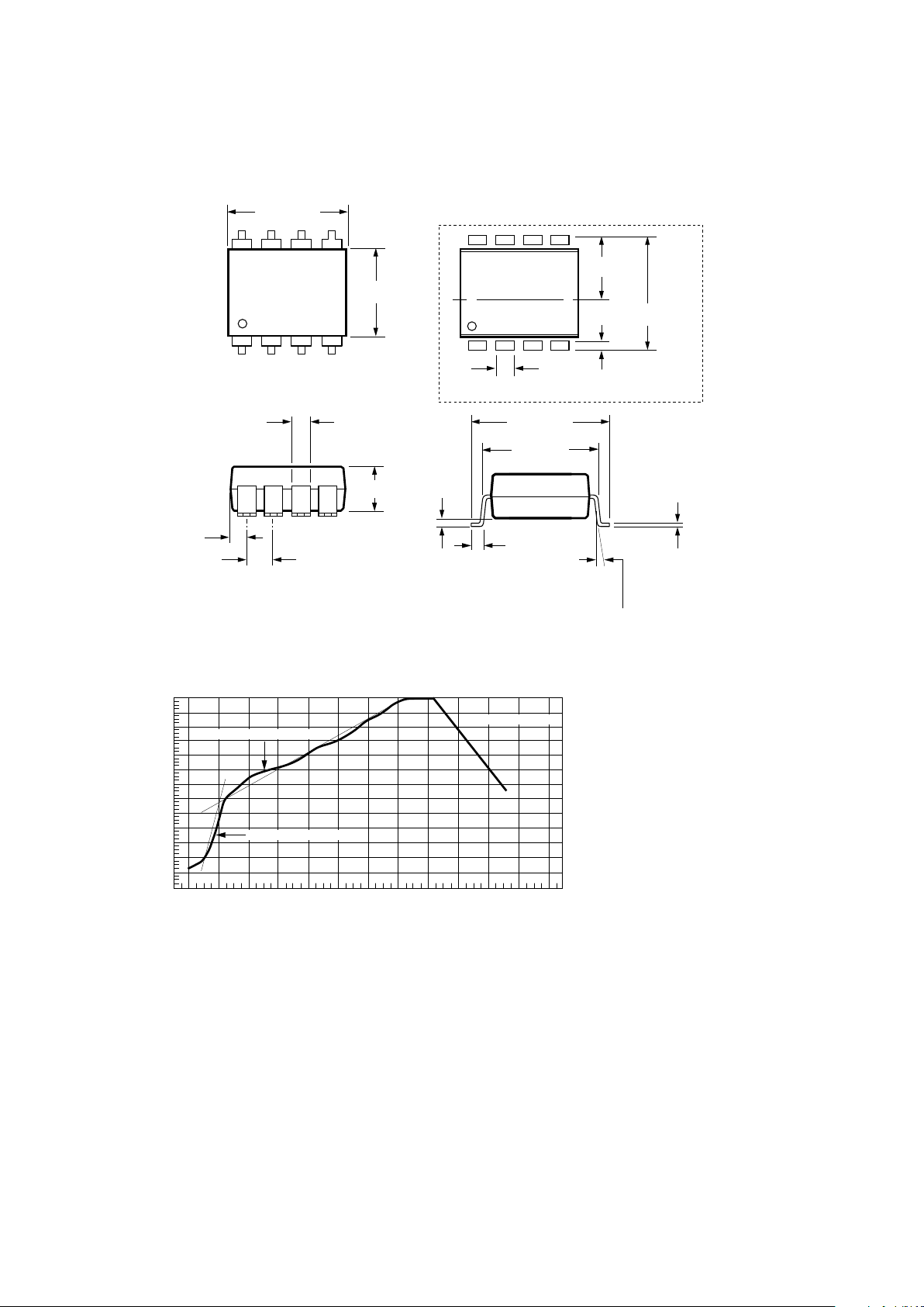
Package Outline Drawings
Figure 1.
0.40 (0.016)
0.56 (0.022)
1
2
3
4
8
7
6
5
1.70 (0.067)
1.80 (0.071)
2.54 (0.100) TYP.
0.51 (0.021) MIN.
5.10 (0.201) MAX.
3.10 (0.122)
3.90 (0.154)
DIMENSIONS IN MILLIMETERS AND (INCHES).
NC
PD1
K
1
11.30 (0.445)
MAX.
PIN
ONE
1.50
(0.059)
MAX.
HP
HCNR200Z
YYWW
OPTION
CODE*
DATE
CODE
8 7 6 5
1
2 3 4
9.00
(0.354)
TYP.
0.20 (0.008)
0.30 (0.012)
0°
15°
11.00
(0.433)
MAX.
10.16
(0.400)
TYP.
K
2
PD2
NC
LED
* MARKING CODE LETTER FOR OPTION NUMBERS.
"V" = OPTION 050
OPTION NUMBERS 300 AND 500 NOT MARKED.
1-420
Gull Wing Surface Mount Option #300
240
∆T = 115°C, 0.3°C/SEC
0
∆T = 100°C, 1.5°C/SEC
∆T = 145°C, 1°C/SEC
TIME – MINUTES
TEMPERATURE – °C
220
200
180
160
140
120
100
80
60
40
20
0
260
123456789101112
(NOTE: USE OF NON-CHLORINE ACTIVATED FLUXES IS RECOMMENDED.)
Maximum Solder Reflow Thermal Profile
Regulatory Information
The HCNR200/201 optocoupler
features a 0.400" wide, eight pin
DIP package. This package was
specifically designed to meet
worldwide regulatory requirements. The HCNR200/201 has
been approved by the following
organizations:
UL Recognized under UL
1577, Component
Recognition Program,
FILE E55361
CSA Approved under CSA
Component Acceptance
Notice #5, File CA
88324
BSI Certification according
to BS415:1994;
(BS EN60065:1994);
BS EN60950:1992
(BS7002:1992) and
EN41003:1993 for Class
II applications
VDE Approved according to
VDE 0884/06.92
(Available Option #050
only)
1.00 ± 0.15
(0.039 ± 0.006)
7° NOM.
12.30 ± 0.30
(0.484 ± 0.012)
0.75 ± 0.25
(0.030 ± 0.010)
11.00
(0.433)
5
6
7
8
4
3
2
1
11.15 ± 0.15
(0.442 ± 0.006)
9.00 ± 0.15
(0.354 ± 0.006)
1.3
(0.051)
12.30 ± 0.30
(0.484 ± 0.012)
6.15
(0.242)
TYP.
0.9
(0.035)
PAD LOCATION (FOR REFERENCE ONLY)
1.78 ± 0.15
(0.070 ± 0.006)
4.00
(0.158)
MAX.
1.55
(0.061)
MAX.
2.54
(0.100)
BSC
DIMENSIONS IN MILLIMETERS (INCHES).
LEAD COPLANARITY = 0.10 mm (0.004 INCHES).
0.254
+ 0.076
- 0.0051
(0.010
+ 0.003)
- 0.002)
MAX.
1-421
VDE 0884 (06.92) Insulation Characteristics (Option #050 Only)
Description Symbol Characteristic Unit
Installation classification per DIN VDE 0110/1.89, Table 1
For rated mains voltage ≤ 600 V rms I-IV
For rated mains voltage ≤ 1000 V rms I-III
Climatic Classification (DIN IEC 68 part 1) 55/100/21
Pollution Degree (DIN VDE 0110 Part 1/1.89) 2
Maximum Working Insulation Voltage V
IORM
1414 V peak
Input to Output Test Voltage, Method b* V
PR
2651 V peak
VPR = 1.875 x V
IORM
, 100% Production Test with
tm = 1 sec, Partial Discharge < 5 pC
Input to Output Test Voltage, Method a* V
PR
2121 V peak
VPR = 1.5 x V
IORM
, Type and sample test, tm = 60 sec,
Partial Discharge < 5 pC
Highest Allowable Overvoltage* V
IOTM
8000 V peak
(Transient Overvoltage, t
ini
= 10 sec)
Safety-Limiting Values
(Maximum values allowed in the event of a failure,
also see Figure 11)
Case Temperature T
S
150 °C
Current (Input Current IF, PS = 0) I
S
400 mA
Output Power P
S,OUTPUT
700 mW
Insulation Resistance at TS, VIO = 500 V R
S
>10
9
Ω
*Refer to the front of the Optocoupler section of the current catalog for a more detailed description of VDE 0884 and other product
safety regulations.
Note: Optocouplers providing safe electrical separation per VDE 0884 do so only within the safety-limiting values to which they are
qualified. Protective cut-out switches must be used to ensure that the safety limits are not exceeded.
Insulation and Safety Related Specifications
Parameter Symbol Value Units Conditions
Min. External Clearance L(IO1) 9.6 mm Measured from input terminals to output
(External Air Gap) terminals, shortest distance through air
Min. External Creepage L(IO2) 10.0 mm Measured from input terminals to output
(External Tracking Path) terminals, shortest distance path along body
Min. Internal Clearance 1.0 mm Through insulation distance conductor to
(Internal Plastic Gap) conductor, usually the direct distance
between the photoemitter and photodetector
inside the optocoupler cavity
Min. Internal Creepage 4.0 mm The shortest distance around the border
(Internal Tracking Path) between two different insulating materials
measured between the emitter and detector
Comparative Tracking Index CTI 200 V DIN IEC 112/VDE 0303 PART 1
Isolation Group IIIa Material group (DIN VDE 0110)
Option 300 – surface mount classification is Class A in accordance with CECC 00802.

1-422
Absolute Maximum Ratings
Storage Temperature .................................................. -55°C to +125°C
Operating Temperature (TA)........................................ -55°C to +100°C
Junction Temperature (TJ) ............................................................125°C
Reflow Temperature Profile ... See Package Outline Drawings Section
Lead Solder Temperature ..................................................260°C for 10s
(up to seating plane)
Average Input Current - IF............................................................ 25 mA
Peak Input Current - IF................................................................. 40 mA
(50 ns maximum pulse width)
Reverse Input Voltage - VR.............................................................. 2.5 V
(IR = 100 µA, Pin 1-2)
Input Power Dissipation ......................................... 60 mW @ TA = 85°C
(Derate at 2.2 mW/°C for operating temperatures above 85°C)
Reverse Output Photodiode Voltage ................................................ 30 V
(Pin 6-5)
Reverse Input Photodiode Voltage................................................... 30 V
(Pin 3-4)
Recommended Operating Conditions
Storage Temperature .................................................... -40°C to +85°C
Operating Temperature ................................................. -40°C to +85°C
Average Input Current - IF....................................................... 1 - 20 mA
Peak Input Current - IF................................................................. 35 mA
(50% duty cycle, 1 ms pulse width)
Reverse Output Photodiode Voltage ........................................... 0 - 15 V
(Pin 6-5)
Reverse Input Photodiode Voltage .............................................. 0 - 15 V
(Pin 3-4)
 Loading...