


Programmable
Frequency Counter
PM6685 & PM6685R
Service Manual
This is a complementary service manual covering instruments with manufacturing numbers exceeding 840684. The principal differences are to be found in Chapter 7 and in Chapter 8 due to a major redesign of the main PCB.
Do not dispose of the previous edition, identified by the part number, 4822 872 25012, and the publishing date, June 1996. You may have to refer to it for information on older instruments as well as options not mentioned here.
4822 872 20106 First Edition (May 2003)
No part of this manual may be copied without the express permission of the copyright owner. All product names are trademarks of their respective companies.
2003 Pendulum Instruments AB All rights reserved. Printed in Sweden.
Contents
1Safety Instructions
2Performance Check
General Information . . . . . . . . . . . . . . . . . . . . . . . . . 2-2
Recommended Test Equipment . . . . . . . . . . . . . . . . 2-2
Front Panel Controls . . . . . . . . . . . . . . . . . . . . . . . . . 2-2
Short Form Specification Test . . . . . . . . . . . . . . . . . . 2-3
Rear Input/Output . . . . . . . . . . . . . . . . . . . . . . . . . . . 2-4
Measuring Functions . . . . . . . . . . . . . . . . . . . . . . . . . 2-4
Options . . . . . . . . . . . . . . . . . . . . . . . . . . . . . . . . . . . 2-5
3 Disassembly
Removing the Cover . . . . . . . . . . . . . . . . . . . . . . . . . 3-2 Reinstalling the Cover . . . . . . . . . . . . . . . . . . . . . . . . 3-2 PM9624 (HF Input) . . . . . . . . . . . . . . . . . . . . . . . . . . 3-2 PM9626B (GPIB Interface) . . . . . . . . . . . . . . . . . . . . 3-3 PM9691 or PM9692 (Oven Oscillator) . . . . . . . . . . . 3-3
4 Circuit Descriptions
Block Diagram Description . . . . . . . . . . . . . . . . . . . . 4-2
General . . . . . . . . . . . . . . . . . . . . . . . . . . . . . . . . . . 4-2
Hardware Functional Description . . . . . . . . . . . . . . . 4-4
Front Unit . . . . . . . . . . . . . . . . . . . . . . . . . . . . . . . . . 4-4
Main Board . . . . . . . . . . . . . . . . . . . . . . . . . . . . . . . . 4-5
Rear Panel Unit . . . . . . . . . . . . . . . . . . . . . . . . . . . . 4-13
Optional Units . . . . . . . . . . . . . . . . . . . . . . . . . . . . . 4-14
Software Functional Description . . . . . . . . . . . . . . 4-15
Test Routines . . . . . . . . . . . . . . . . . . . . . . . . . . . . . 4-16
5 Repair
Preventive Maintenance. . . . . . . . . . . . . . . . . . . . . . . 5-2
Calibration . . . . . . . . . . . . . . . . . . . . . . . . . . . . . . . . . 5-2
When to Replace the Fan
(PM6685R only ) . . . . . . . . . . . . . . . . . . . . . . . . . . . . 5-3
Troubleshooting . . . . . . . . . . . . . . . . . . . . . . . . . . . . . 5-4
General . . . . . . . . . . . . . . . . . . . . . . . . . . . . . . . . . . . 5-4
Safety Inspection and Test After Repair . . . . . . . . . 5-9
General Directives. . . . . . . . . . . . . . . . . . . . . . . . . . . 5-9
6 Calibration Adjustments
Introduction . . . . . . . . . . . . . . . . . . . . . . . . . . . . . . . . 6-2
Preparation . . . . . . . . . . . . . . . . . . . . . . . . . . . . . . . . 6-2
Power Supply . . . . . . . . . . . . . . . . . . . . . . . . . . . . . . 6-2
Input Amplifier . . . . . . . . . . . . . . . . . . . . . . . . . . . . . . 6-3
Reference Oscillators . . . . . . . . . . . . . . . . . . . . . . . . 6-4
Other Options . . . . . . . . . . . . . . . . . . . . . . . . . . . . . . 6-6
7 Replacement Parts
Introduction . . . . . . . . . . . . . . . . . . . . . . . . . . . . . . . . 7-2
Mechanical Parts. . . . . . . . . . . . . . . . . . . . . . . . . . . . 7-3
Main Board . . . . . . . . . . . . . . . . . . . . . . . . . . . . . . . . 7-6
Front Board . . . . . . . . . . . . . . . . . . . . . . . . . . . . . . . 7-12
GPIB Interface (PM9626B) . . . . . . . . . . . . . . . . . . . 7-13
8 Drawings & Diagrams
How to read the diagrams. . . . . . . . . . . . . . . . . . . . . 8-2
9 Appendix
How to Replace Surface Mounted Devices. . . . . . . . 9-2 Electrostatic discharge . . . . . . . . . . . . . . . . . . . . . . . 9-3 Glossary . . . . . . . . . . . . . . . . . . . . . . . . . . . . . . . . . . 9-4
Power Supply Switchmode Module . . . . . . . . . . . . . 9-5
Circuit Descriptions . . . . . . . . . . . . . . . . . . . . . . . . . . 9-5 Repair . . . . . . . . . . . . . . . . . . . . . . . . . . . . . . . . . . . . 9-6 Calibration Adjustments . . . . . . . . . . . . . . . . . . . . . . 9-7 Replacement Parts. . . . . . . . . . . . . . . . . . . . . . . . . . 9-8
PM6685R . . . . . . . . . . . . . . . . . . . . . . . . . . . . . . . . . . 9-12
Introduction . . . . . . . . . . . . . . . . . . . . . . . . . . . . . . . 9-12 Performance Check . . . . . . . . . . . . . . . . . . . . . . . . 9-12 Functional Description. . . . . . . . . . . . . . . . . . . . . . . 9-12 Calibration Adjustments . . . . . . . . . . . . . . . . . . . . . 9-13 Replacement Parts . . . . . . . . . . . . . . . . . . . . . . . . . 9-14
This page is intentionally left blank.
Chapter 1
Safety Instructions
WARNING: These servicing instructions are for use by qualified personnel only. To reduce the risk of electric shock, do not perform any servicing other than that specified in the Operating Manual unless you are fully qualified to do so.
Authorized service and calibration of this instrument is available through your Fluke representative. See address at the end of this manual.
Read this chapter carefully before you check, adjust, or repair an instrument.
Caution and Warning Statements
You will find specific warning and caution statements where necessary throughout the manual.
CAUTION: Indicates where incorrect operating procedures can cause damage to, or destruction of, equipment or other property.
WARNING: Indicates a potential danger that requires correct procedures or practices in order to prevent personal injury.
This Timer/Counter has been designed and tested in accordance with safety class 1 requirements for Electronic Measuring Apparatus of IEC (CENELEC) publication EN61010-1, and CSA 22.2 No. 1010-1, and has been supplied in a safe condition.
This manual contains information and warnings that should be followed by the user and the service technician to ensure safe operation and repair in order to keep the instrument in a safe condition.
WARNING: Opening instrument covers or removing parts, except those to which access can be gained by hand, is likely to expose high voltages which can cause death.
The instrument must be disconnected from all voltage sources before it is opened. Remember that the capacitors inside the instrument retain their charge even if the instrument has been disconnected from all voltage sources.
Grounding
This instrument is connected to ground via a sealed three-core power cable, which must be plugged into socket outlets with protective ground contacts. No other method of grounding is permitted for this instrument.
The ground symbol on the rear panel indicates where the protective ground lead is connected inside the instrument. Never remove or loosen this screw.
When the instrument is brought from a cold to a warm environment, condensation may cause hazardous conditions. Therefore, ensure that the grounding requirements are strictly met.
Power extension cables must always have a protective ground conductor.
Indicates that the operator should consult the manual.
WARNING: Any interruption of the protective ground conductor inside or outside the instrument, or disconnection of the protective ground terminal, is likely to make the instrument dangerous. Do not intentionally disrupt the protective grounding.
Disposal of Hazardous Materials
WARNING: Disposal of lithium batteries requires special attention. Do not expose the batteries to heat or put them under extensive pressure. These measures may cause the batteries to explode.
A lithium battery is used to power the nonvolatile RAM in this instrument. Our world suffers from pollution, so don’t throw batteries into your wastebasket. Return used batteries to your supplier or to the Fluke representative in your country.
Line Voltage
The instrument can be powered by any voltage between 90 and 265 VAC without range switching. This makes it suitable for all nominal line voltages between 100 and 240 V.
Replacing Components in Primary Circuits
Components that are important for the safety of this instrument may only be replaced by components obtained from your local Fluke representative. After exchange of the primary circuits, perform the safety inspection and tests, as described in Chapter 5, “Repair”.
Fuses
This instrument is protected by an ordinary 1.6 A slow blow fuse mounted inside the instrument. NEVER replace this fuse without first examining the Power Supply Unit.
1-2 Safety Instructions,
Chapter 2
Performance Check

General Information
WARNING: Before turning on the instrument, ensure that it has been installed in accordance with the Installation Instructions outlined in Chapter 3 of the Operators Manual.
This performance procedure is intended to:
–Check the instrument’s specification.
–Be used for incoming inspection to determine the acceptability of newly purchased instruments and recently recalibrated instruments.
–Check the necessity of recalibration after the specified recalibration intervals.
NOTE: The procedure does not check every facet of the instrument’s calibration; rather, it is concerned primarily with those parts of the instrument which are essential for determining the function of the instrument.
It is not necessary to remove the cover of the instrument to perform this procedure.
If the test is started less than 20 minutes after turning on the instrument, results may be out of specification, due to insufficient warm-up time.
Recommended Test
Equipment
Type of instru- |
|
Required |
Suggested |
ment |
|
Specifications |
Equipment |
LF Synthesizer |
Square; |
|
|
|
Sine up to 10 MHz |
|
|
Power Splitter |
50 |
|
PM9584/02 |
T-piece |
|
|
|
Termination |
50 |
|
PM9585 |
Reference oscilla- |
10 |
MHz ±0.1 Hz for |
Fluke counter with |
tor |
standard oscillator |
calibrated option |
|
|
|
|
PM9691 |
|
10 |
MHz ±0.01 Hz for |
Fluke PM6685R or |
|
PM9691 & PM9692 |
PM6681R |
|
|
10 |
MHz ±0.0001 Hz |
Fluke 910R or Ce- |
|
for PM6685R |
sium Standard |
|
HF signal genera- |
0.5 GHz (no presc.) |
|
|
tor |
3.3 GHz (option 10) |
|
|
Pulse Generator |
125 MHz |
|
|
Oscilloscope with |
350 MHz |
|
|
probes |
|
|
|
BNC cables |
5 to 7 cables * |
|
|
|
|
|
|
Table 2-1 Recommended Test Equipment.
*) Two of the cables must have 10 ns difference in delay, for example: 5 ns and 15 ns.
Preparations
Power up your instruments at least 20 minutes before beginning the tests to let them reach normal operating temperature. Failure to do so may result in certain test steps not meeting equipment specifications.
Front Panel Controls
Power-On Test
At power-on the counter performs an automatic self-test of the following:
–Microprocessor
–RAM
–ROM
–Measuring circuits
–Display
If a GPIB interface is installed, the GPIB address is displayed.
If there are any test failures, an error message is shown.
–Turn on the counter and check that all segments light up on the display and that no error message appears.
Ω |
Fig. 2-1 Text on the display.
Internal Self-Tests
The different built-in test routines invoked by the power-on test can also be activated from the front panel as follows:
–Enter the Auxiliary Menu by pressing AUX MENU.
–Select the test submenu by pressing DATA ENTRY up or down.
–Enter the test menu by pressing the ENTER key. Selections for internal self-tests are:
1TEST ALL (Test 2 to 5 in sequence)
2TEST RO (ROM)
3TEST RA (RAM)
4TEST LOGIC (Measuring Logic)
5TEST DISP (Display Test)
–Use DATA ENTRY up/down to select TEST ALL, then press
ENTER.
–If any fault is detected, an error message appears on the display and the program halts.
–If no faults are detected, the program returns to measuring mode.
2-2 Performance Check, General Information

Keyboard Test
The keyboard test verifies that the counter responds when you press any key. To check the function behind the keys, see the tests further on in this chapter.
Press the keys as described in the left column and look on the display for the text, as described in the second column. Some keys change more text on the display than described here. The display text mentioned here is the text mainly associated with the selected key.
Key(s) |
|
Display |
Note |
Pass |
|
|
|
|
|
|
/Fail |
STAND-BY |
|
Display Off |
Red LED |
|
|
|
|
|
|
beside |
|
|
|
|
|
the key |
|
|
|
|
|
On |
|
ON |
|
Backlight on |
|
|
|
PRESET |
|
DEFAULT? |
Default |
|
|
ENTER |
|
NO SIGNAL |
setting |
|
|
EXT REF |
|
EXT REF |
|
|
|
Input A |
|
|
|||
FILTER |
|
FILTER |
|
|
|
50 |
|
50 |
|
|
|
|
|
|
|
|
|
|
|
|
|
|
|
(2 times) |
|
|
|
|
|
SENS |
|
Bar graph: |
|
|
|
(2 times) |
|
|
|
|
|
SENS |
|
Bar graph: |
|
|
|
(2 times) |
|
|
|
|
|
AUTO |
|
AUTO TRIG |
|
|
|
Other |
|
|
|||
PRESET |
|
DEFAULT? |
Default |
|
|
ENTER |
|
NO SIGNAL |
setting |
|
|
MEAS TIME |
|
200–3 s |
|
|
|
DATA ENTRY |
|
500–3 s |
|
|
|
DATA ENTRY |
|
200–3 s |
|
|
|
ENTER |
|
NO SIGNAL |
|
|
|
DISPLAY HOLD |
|
HOLD |
|
|
|
DISPLAY HOLD |
|
|
|
|
|
SINGLE |
|
SINGLE |
|
|
|
FUNCTION |
|
DUTY F A |
|
|
|
FUNCTION |
|
TOT A MAN |
|
|
|
FUNCTION |
|
DUTY F A |
|
|
|
FUNCTION |
|
FREQ A |
|
|
|
AUX MENU |
|
RECALL |
|
|
|
MEAS RESTART |
|
NO SIGNAL |
|
|
|
PRESET |
|
DEFAULT? |
Default |
|
|
ENTER |
|
NO SIGNAL |
setting |
|
|
CHECK |
|
10.000000006Hz* |
Start |
|
|
|
|
|
|
counting |
|
NULL |
|
NULL |
|
|
|
NULL |
|
10.000000006Hz* |
|
|
|
BLANK DIGITS |
|
10.00000 6Hz* |
|
|
|
(3 times) |
|
|
|
|
|
MENU |
|
Displays all avail- |
|
|
|
|
|
able functions, pro- |
|
|
|
|
|
cesses and input |
|
|
|
|
|
controls. Selected |
|
|
|
|
|
items are blinking. |
|
|
|
|
|
|
|
|
|
Table 2-2 Keyboard Test.
NOTE: For the instrument to respond correctly, this test must be carried out in sequence and you must start with the preset (power-on) setting.
*The LSD may vary.
**MENU is not disabled by setting DEFAULT; press menu again.
Short Form Specification
Test
Sensitivity and Frequency Range
–Press the PRESET key to set the counter in the default setting. Then confirm by pressing ENTER.
–Turn off AUTO.
–Select IMP A = 50 and maximum sensitivity.
–Connect a signal from a HF generator to a BNC power splitter.
–Connect the power splitter to your counter and an oscilloscope.
–Set input impedance to 50 on the oscilloscope.
–Adjust the amplitude according to the following table. Read the level on the oscilloscope. The counter should display the correct frequency.
Frequency |
|
Level |
|
Pass/Fail |
MHz |
mVPP |
mVRMS |
dBm |
Input A |
1 |
30 |
10 |
–27 |
|
25 |
30 |
10 |
–27 |
|
50 |
30 |
10 |
–27 |
|
150 |
60 |
20 |
–21 |
|
200 |
90 |
30 |
–17 |
|
250 |
150 |
50 |
-13 |
|
300 |
150 |
50 |
-13 |
|
|
|
|
|
|
Table 2-3 Sensitivity of input A at various frequencies.
Reference Oscillators
X-tal oscillators are affected by a number of external conditions, such as ambient temperature and supply voltage, but they are also affected by aging. Therefore, it is hard to give limits for the allowed frequency deviation. You must decide the limits depending on your application, and recalibrate the oscillator accordingly. See the Preventive Maintenance in the Repair chapter, Chapter 5.
Oscillator |
Max. tempera- |
Max. aging |
Max. aging |
|
ture dependence |
per month |
per year |
Standard |
±100 Hz |
±5 Hz |
±50 Hz |
PM9691 |
±0.05 Hz |
±0.1 Hz |
±0.75 Hz |
PM9692 |
±0.025 Hz |
±0.03 Hz |
±0.2 |
Rubidium |
±0.003 Hz |
±0.0005 Hz |
±0.002 Hz |
|
|
|
|
Table 2-4 Deviation (for PM9691 and PM9692 after a warm-up period of 48 hours).
To check the accuracy of the oscillator you must have a calibrated reference signal that is at least five times as stable as the oscillator that you are testing, see the following table.
–Press the PRESET key, then press the ENTER key to set your counter in the Default setting.
Performance Check, Short Form Specification Test 2-3
–Connect the reference to input A.
–Check the readout against the accuracy requirements of your application.
Acceptance Test
As an acceptance test, the following table gives a worst case figure after a 30 minute warm up time. All deviations that can occur in a year are added together.
Oscillator |
Frequency readout |
Suitable refer- |
Pass |
|
|
ence |
/Fail |
Standard |
10.00000000 MHz |
PM9691 |
|
|
±120 Hz |
|
|
PM9691 |
10.00000000 MHz |
|
|
|
±1 Hz |
PM6685R |
|
PM9692 |
10.00000000 MHz |
PM6681R |
|
|
|
||
|
±0.25 Hz |
|
|
|
|
|
|
Table 2-5 Acceptance test for oscillators. |
|
||
Acceptance Test, PM6685R
To fully test the accuracy of the PM6685R, a reference signal of extremely high stability is needed. Examples of such references are Cesium Atomic references, or transmitted signals from a nationally or internationally traceable source, like the GPS satellites.
Recommended Test Equipment
Type |
Stability |
Model |
10 MHz refer- |
1x10⁻¹⁰ |
910R with satellite contact dur- |
ence |
|
ing the last 72 hours. |
|
|
|
Test Procedure
–Connect the counter to the line power.
–Check that the UNLOCK indicator turns on, and then turns off again within 6 minutes after connecting line power.
–Connect the 10 MHz reference signal to input A of the counter.
–Select FREQUENCY A measurement.
–Select 2 s measuring time.
–Check that the displayed frequency is 10.00000000 MHz ±0.05 Hz 10 minutes after connection to line power.
Rear Input/Output
INT REF Output
–Connect an oscilloscope to the 10 MHz output on the rear of the counter. Use coaxial cable and 50 termination.
–The output voltage is sinusoidal and should be above 2.8 VPP.
EXT REF Input
–Press the PRESET key, then press the ENTER key to set your counter in the Default setting.
–Apply 10 MHz sine to input A equipped with a T-piece and to Ext Ref input at the rear, terminated with 50 . Amplitude on 10 MHz signal; 200 mVRMS, (560 mVPP)
–Press the Ext Ref key.
–The display should show 10.000000006 Hz ± 5 LSD.
EXT ARM INPUT
–Press the PRESET key, then press the ENTER key to set your counter in the Default setting.
–Select 50 input impedance.
–Apply 10 MHz 500 mVRMS, (1.4 VPP) sine to input A
–The counter measures and displays 10 MHz.
–Press the AUX MENU key.
–Press the DATA ENTRY UP/DOWN keys until the display shows ‘Ar. Start’, confirm by pressing the ENTER key.
–Press DATA ENTRY UP/DOWN keys until the display shows ‘POS’, confirm by pressing the ENTER key.
–Press the ENTER key once more.
–The counter does not measure.
–Connect a pulse generator to Ext Arm input.
–Settings for pulse generator: single shot pulse, amplitude TTL = 0 - 2 VPP, and duration = 10 ns.
–Apply one single pulse to Ext Arm input.
–The counter measures once and shows 10 MHz on the display.
Measuring Functions
Preparation for Check of Measuring Function is as follows:
–Connect a 10 MHz sine wave signal with 2.0 VPP amplitude via a T-piece to Input A.
–Connect a cable from the T-piece to Input E (Ext Arm) at the rear.
–Select the measuring function as in the ‘Selected Function’ column and check that the counter performs the correct measurement by displaying the result as shown under the “Display” column in the following table.
Selected Function |
Display |
Pass/ Fail |
PRESET |
DEFAULT? |
|
ENTER |
10 MHz 2) |
|
IMP A 50 |
10 MHz 2) |
|
Non AUTO |
10 MHz 2) |
|
PER A |
100 ns 2) |
|
RATIO A/E |
1.0000000 |
|
PWIDTH A |
50 ns 1) |
|
TOT A MAN |
|
|
DISPLAY HOLD |
Start counting |
|
DISPLAY HOLD |
Stop counting |
|
DUTY FACT |
0.500000 1) |
|
AUTO |
0.500000 1) |
|
|
|
|
Table 2-6 Measuring functions check.
1)Value depends on the symmetry of the signal.
2)Exact value depends on the input signal.
2-4 Performance Check, Rear Input/Output
Options
Prescaler
This extra HF input (PM9624) is easily recognized by its front panel connector (Input C, type N).
EX T |
RE F |
Fig 2-2 Connect the output of the signal generator to the HF input of the counter.
Required Test Equipment |
Suggested Specification |
HF signal generator |
3.3 GHz |
|
|
Table 2-8 Test equipment for 3.0 GHz HF input.
–Connect the output of the signal generator to the HF input of the counter.
–Connect the 10 MHz REFERENCE OUT of the generator to the REFERENCE IN at the rear panel of the counter.
Setting for the counter after Preset.
–Function = FREQ C.
–EXT REF.
Generate a sine wave in accordance with the following table.
–Verify that the counter counts correctly. (The last digit will be unstable).
Frequency |
Amplitude |
Pass/Fail |
|
MHz |
mVRMS |
dBm |
|
100-300 |
20 |
–21 |
|
-2500 |
10 |
–27 |
|
-2700 |
20 |
–21 |
|
-3000 |
100 |
–7 |
|
|
|
|
|
Table 2-7 Sensitivity of the PM9624 HF input.
Performance Check, Options 2-5
This page is intentionally left blank.
2-6 Performance Check, Options
Chapter 3
Disassembly
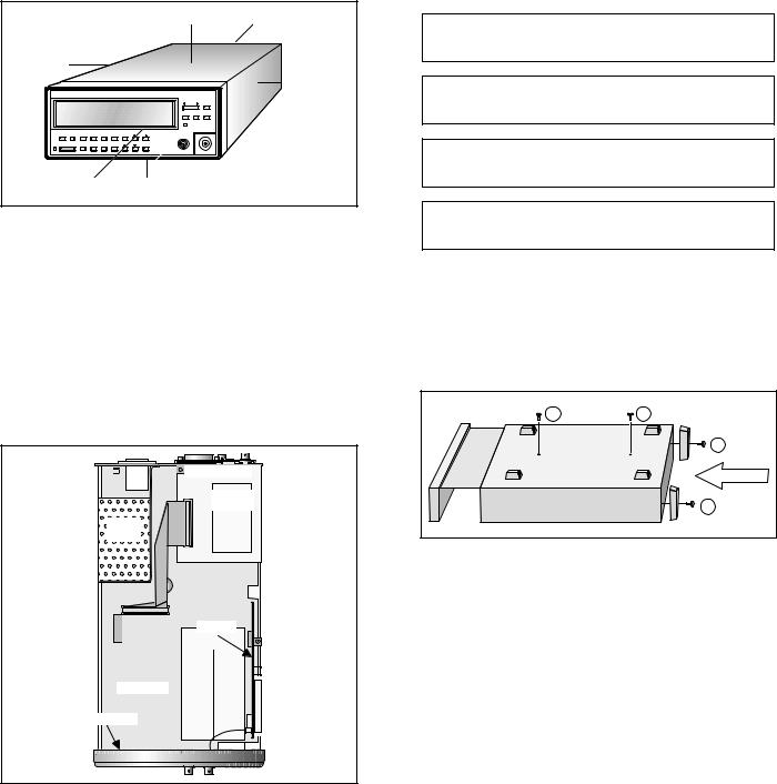
The terms in the following figure are used in all descriptions in this manual.
Top Rear
Left
Right
Front Bottom
Fig. 3-1 Designations used in this manual.
The PM6685 is available with a number of options and accessories. The labels on the rear panel of the counter identify the options and accessories included. If there are no labels, the counter contains an uncompensated crystal oscillator and no options. The following labels exist:
–PM9624 3.0 GHz HF input
–PM9691 High-Stability Oven Oscillator
–PM9692 Ultra-High-Stability Oven Oscillator
–PM9626B GPIB Interface
The location of these optional parts is illustrated in Fig.3-2.
GPIB interface |
Optional |
oscillator |
Power |
Module |
G 1 |
HF input |
Main board |
Front panel |
Fig. 3-2 Location of the boards in the counter.
Removing the Cover
WARNING: Do not perform any internal service or adjustment of this instrument unless you are qualified to do so.
WARNING: When you remove the cover you will expose high voltage parts and accessible terminals which can cause death.
WARNING: Although the power switch is in the off position, line voltage is present on the printed circuit board. Use extreme caution.
WARNING: Capacitors inside the instrument can hold their charge even if the instrument has been separated from all voltage sources.
–Make sure the power cord is disconnected from the counter.
–Turn the counter upside down.
–Loosen the two screws (A) at the bottom and the two screws
(B)in the rear feet.
–Grip the front panel and gently push at the rear.
–Pull the counter out of the cover.
A |
A |
|
B |
|
B |
Fig. 3-3 Remove the screws and push the counter out of the cover.
Reinstalling the Cover
–Gently push the counter back into the cover.
–Turn it upside down.
–Install the two screws (A) at the bottom.
–Install the two rear feet with the screws (B) to the rear panel.
PM9624 (HF Input)
–Disconnect the power cable.
–Remove the cover from the counter.
–Disconnect the cable from the mini-coax connector (A) on the HF input.
–Press the clips (B) apart and lift the HF input pca straight up and out.
3-2 Disassembly, Removing the Cover

–When installing the HF input, make sure that the connector pins fit exactly in the holes in the connector housing (C).
A |
B |
C |
B |
Fig. 3-6 Removing the HF Input.
PM9626 (GPIB Interface)
–Disconnect the power cable.
–Remove the cover from the counter.
–Loosen the two screws (A) holding the GPIB interface to the rear panel.
–Disconnect the interface cable from P103.
–Move the GPIB interface pca toward the front of the counter and lift the pca supports out from the “keyholes” (B) on the main PCA.
|
A |
A |
|
|
|
B |
|
B |
Fig. 3-4 Loosen the two screws in the rear panel and disengage the board from the keyholes.
PM9691 or PM9692 (Oven Oscillator)
–Disconnect the power cable.
–Remove the cover of the counter.
–Remove the two screws (A) holding the oscillator to the main pca from underneath.
–Press the clip (B) gently to the front of the counter and lift the oscillator straight up.
–Make sure that jumpers J14 and J15 are set in the correct position.
–When fitting the oscillator, make sure that the connector pins fit exactly in the holes in the connector housing.
A |
Fig. 3-5 One of the two screws holding the oven oscillator in place.
Disassembly, PM9626 (GPIB Interface) 3-3
This page is intentionally left blank.
3-4 Disassembly, PM9691 or PM9692 (Oven Oscillator)
Chapter 4
Circuit Descriptions
Block Diagram Description
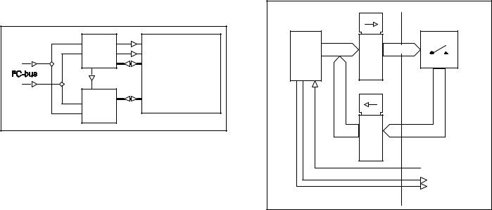
General
The PM6685 Frequency Counter consists of three main units:
–Front unit
–Main board unit
–Rear panel unit
The following options can be added:
–GPIB interface including analog output (PM9626B)
–Prescalers 1.3 GHz (PM9621), 3.0 GHz (PM9624)
–Oven-controlled crystal oscillators (PM9691 or PM9692)
–Rack mount adapter (PM9622/02)
–Battery option (PM9623)
The chassis of the counter consists of a front piece molded in aluminum, an aluminum rear panel, and two profiled aluminum rods that hold the front and rear panels together. This unit can be slid into the aluminum cover of the instrument.
The front unit contains all functions needed for the user communication. It is connected to the main board unit with a flat cable, and the
molded front unit is fixed to the two profiled aluminum rods with screws.
The main board unit consists of a PCB mounted on two profiled aluminum rods. Most functions, such as the following, are placed on the main board:
–Input amplifiers with trigger level circuits
–Power supply
–Measurement logic
–Microcomputer circuitry
Some outputs, such as the trigger levels and probe compensation view outputs are directly mounted on the main board.
The rear panel unit is of aluminum with a number of mounted connectors. Most of the connectors are soldered directly to the main board. The rear panel is fixed to the two profiled aluminum rods with screws.
4-2 Block Diagram Description

|
|
|
X2 |
INTREF |
G |
|
Optional oscillator |
|
10 MHz out |
||
|
|
|
EXTC |
|
|
|
|
|
B2 |
|
|
E |
|
|
EXTREF |
|
|
External arming |
|
A |
|
|
|
|
|
|
|
||
|
|
÷2 |
A2 |
|
|
C |
HF input |
|
|
U29 |
|
|
|
Counter |
|
||
|
|
|
|
||
|
|
|
GET |
|
|
|
|
|
ASIC |
|
|
|
|
|
|
|
|
D |
External reference |
|
|
|
|
|
|
|
|
|
|
A |
Input Amplifier |
|
|
|
|
|
|
|
|
|
|
|
|
|
Micro- |
|
|
|
|
|
computer |
|
|
|
Trigger DAC´s |
|
U11 |
|
Gate LED |
|
|
|
|
|
|
|
|
|
|
|
I2C |
|
Local preset |
|
HSI.0 |
|
Display |
|
|
|
|
||
|
Reset circuit |
|
RESET |
|
PWM |
|
|
|
Analog output |
||
|
|
|
|
|
Option 80 |
|
Power supply |
+5V |
|
|
GPIB option |
|
|
|
|
||
AC |
90-265 V |
+12V |
|
|
|
|
|
+7V |
|
|
|
|
|
-5.2V |
|
|
|
|
|
|
|
|
Keyboard |
Fig. 4-1 |
PM6685 block diagram. |
|
|
|
|
Block Diagram Description 4-3
Hardware Functional Description
Front Unit
LCD Drivers
|
U 20 1 |
|
Backpl. 0 |
|
Dr iver 1 |
||
|
Backpl. 1 |
||
|
PC F8 |
576 |
|
|
|
||
SCL |
|
|
|
|
|
|
LC D |
SD A |
Sync. |
1 58 segment s |
|
|
|
||
|
U2 02 |
|
2:1 Multiplex |
|
|
|
|
|
Dr iver 2 |
|
|
|
PC F 8576 |
|
|
Fig. 4-2 Front panel LCD drivers.
An LCD and two LEDs are used as indicators. The LCD is used to show both the measurement result and the state indicators of the instrument setting. The LEDs show standby and gating.
The LCD has 158 segments that are multiplexed with a ratio of 2:1. Two parallel and synchronized LCD drivers (U201 and U202) are used. They are connected with a serial I2C bus to the microcomputer on the main board. The clock frequency of the drivers is approximately 140 kHz, set by R201. The VLCD pin is connected to GND on the main board.
The LCD is provided with a backlight, an LED array integrated into one component. Its current consumption is set by the resistors R204-R207. The backlight dissipates approximately 1.5 W .
Keyboard
Main Board |
U13A |
Keyboard & Display |
|
Latch |
|||
|
Board |
|
U11 |
|
|
|
|
AD0-AD7 |
H0-H3 |
|
CPU |
|
|
P1.0 |
P1.1 |
HS1.0 |
|
|
|
-AD7 |
U14A |
|
|
Latch |
|
|
|
AD0 |
|
|
|
|
|
|
|
|
V0-V7 |
|
|
|
LOCAL/PRESET |
|
|
|
SCL |
|
|
|
SDA |
Fig. 3 Keyboard scanning.
The front panel pushbuttons are connected in a matrix. The scanning signals H0 to H3 come from the main board. If a push button is pressed and H0 to H3 is high, one of the output signals V0 to V7 will be high. The STAND-BY/ON and LOCAL-PRESET buttons are not part of the scanning but are connected directly to the main board.
The front unit is fixed to the main board unit with three screws. The electrical connection is made with a 40-lead flat cable to the main board.
4-4 Hardware Functional Description
Main Board
Introduction
Components not necessary for explaining the function are omitted from the figures in this chapter. For the complete set of components, see the circuit diagrams in Chapter 8, Drawings and Diagrams.
Input Amplifier
The input amplifier has 300 MHz bandwidth and is of the split-band type. It contains four main stages: the signal adaptation stage, the impedance converter stage, the comparator stage, and the buffer stage.
Signal Adaptation
This part of the amplifier contains:
– 50 /1 M impedance selector |
|
|
|
|
|||
– x1/x11 attenuator |
|
|
|
|
|
|
|
– Voltage limiter |
|
|
|
|
|
|
|
50 / 1 M Impedance Selector |
|
|
|
||||
|
|
|
K2 |
|
|
|
|
|
|
|
R6 |
C2 |
|
|
|
|
|
|
|
|
|
|
|
|
|
|
C1 |
|
|
|
To V olt age |
J 1 |
|
|
|
|
|
C3 |
|
R1 |
R2 |
R3-R5 |
R22-R23 |
|
li mi ter |
||
|
|
||||||
|
K 1 |
|
|
R18 |
R24- |
|
R27- |
|
|
|
R26 |
|
R28 |
||
|
|
|
|
|
|
||
|
R7-R17 |
|
|
K3 |
|
|
|
|
|
|
|
R19- |
|
|
|
|
|
|
|
R20 |
|
|
|
Fig. 4-4 Impedance selector and 1X/11X attenuator.
The 50 or 1 M impedance modes are selected by relay K1. 50 is selected via the resistors R7 to R17, if the relay is closed. 1 M is
selected if the relay is open. Depending on selected attenuation, the 1 M input impedance is determined by different combinations of resistors.
In x1 attenuation mode (K2 is closed and K3 is open) the impedance is determined by resistor network R22 to R28.
In x11 attenuation mode (K2 is open and K3 is closed) the same network as in the x1 case is involved plus the resistors R3 to R5 and R18 to R20.
The input capacitance in parallel with 1 M is 24 pF at x1 attenuation and 12 pF at x11 attenuation.
The series resistor R1 immediately after the selector serves both as current limiter together with the voltage limiter (see below) and as impedance matching resistor. The resistor also improves the Volt- age-Standing-Wave-Ratio (VSWR) of the amplifier input.
x1/x11 Attenuator
The x1 attenuator consists of a resistive low-frequency divider, which reduces the input signal by a factor of 2, and a capacitive high-frequency divider. The attenuator is formed by the resistors R22-R23 and R24-R26 in parallel with R27-R28. The capacitive part is formed by the variable capacitor C2 in parallel with R22-R23, and the parasitic capacitance across R24-R26.
The capacitive attenuator is adjusted via variable capacitor C2 to the same attenuation value as the resistive attenuator.
The x11 attenuator also consists of a resistive low-frequency divider and a capacitive high-frequency divider. The resistive part is formed by R1-R5, and R18-R20 in parallel with 1 M (the x1 attenuator impedance). The capacitive divider is formed by the variable capacitor C1 and the parasitic capacitance at the node where R5, R18 and R22 meet.
Resistors R2 and R6 improve the frequency response.
Input A |
Imp. |
Trigger |
level Comp I |
Trigger
level Comp II
|
|
Imp. |
Att. |
Limiter |
Conv. |
|
|
LP |
|
filter |
Comp- |
|
arator |
Comp-
arator
Flip- |
Buffer |
A |
Flop |
|
|
÷2 
 Buffer
  A2
A2
Fig. 4-5 Input amplifier block diagram.
Hardware Functional Description 4-5

Voltage limiter
 +5
+5
R35
D1 |
D3 |
From |
To Impedance |
Attenuator |
converter stage |
D2 |
D4 |
R36
 -5.2
-5.2
Fig. 4-6 Voltage limiter.
and D3 to clamp positive voltage and resistor R36 plus the diodes D2 and D4 to clamp negative voltage. The clamp voltage is approximately ±2.1 V for low frequency signals. At high frequency the clamp voltage rises to approximately ±2.3 V.
Impedance Converter Stage
The analog signal from the input stage is fed to an amplifier stage where split-band technique is used to get good frequency response over a wide range. This means that the high-frequency contents of the signal are fed to a high-impedance AC-coupled FET transistor stage Q1. The low-frequency contents are fed to a DC-coupled operational amplifier stage with negative feedback from the output of the converter stage buffer. The low-frequency path handles frequencies up to approximately 5 kHz.
The high-frequency signal is fed to the gate of Q1. The high impedance at the gate is converted to a low impedance at the source. The source is connected to the base of HF transistor Q2, the summing point for the two signal paths.
To make the FET work well in its active region within the whole dynamic range, the FET drain is supplied with +7 V via resistor R42.
The low-frequency signal is divided by the two resistors R27 and R28 before it is coupled to the input pin #2 of the operational amplifier U1. The resistors R37 and R38 at the operational amplifier output pin #6 center the output swing, and capacitor C6 stabilizes the operational amplifier stage.
A voltage limiter that protects the impedance converter against overvoltage is placed between the attenuator and the impedance converter. The voltage limiter consists of resistor R35 and the diodes D1
The low-frequency path goes from the operational amplifier to the base of transistor Q3, the collector of which is connected to the base
+ 7 |
+ 5 |
+ 5 |
Fr om Pro tec tio n ci rcu its
R27
R28
R32
|
R42 |
R43 |
C13 |
Q1 |
Q2 |
|
|
|
Q13 |
C20 |
|
|
|
|
|
|
|
|
R33 |
|
|
R50 |
|
U8 |
-5 .2 |
|
R105 |
|
T o |
|
|
|
|
|||
C5 |
|
K4 |
|
K4 |
Fli p- Fl o p |
|
|
|
+ |
||
|
|
|
L1 |
- |
|
|
|
|
|
+ |
|
|
|
R46 |
C18- |
|
|
|
|
|
- |
||
U1 |
Q3 |
Q4 |
C19 |
|
|
|
R37 |
|
R106 |
|
R29- |
R38 |
C6 |
R47 |
|
R30 |
||||
|
|
|
|
|
- 5 .2 - 5.2 |
-5 .2 |
-5 .2 |
-5 .2 |
Trig |
|
|
|
L e ve l |
|||||
R31 |
|||||||
|
|
|
|
|
Fig. 4-7 Impedance converter.
4-6 Hardware Functional Description
of transistor Q2. This point is common to the high and low frequency paths.
A buffer amplifier with high driving capacity is used to get a linear output in the 100 load resistor R106 over a swing of 2 V. This amplifier consists of a driver stage Q2, an output stage Q13, and a current generator Q4.
From the output of this second amplifier stage, the signal is fed back to the op amp pin 3 via the divider chain R29 to R32. The trimmer potentiometer R31 sets the gain of the low-frequency path equal to the high-frequency gain of about 0.9. Capacitor C5 is connected to operational amplifier pins #1 and #8 to achieve stable operation. The trimmer potentiometer R33 between pins #1 and #5 on the operational amplifier is used for adjusting the offset voltage of the operational amplifier.
The channel A filter connected to the output of the second amplifier stage is a 100 kHz low-pass LC filter. It consists of the coil L1 and the two capacitors C18 and C19 in parallel. The filter is controlled by the relay K4. The filter output is connected to the input of the comparator stage.
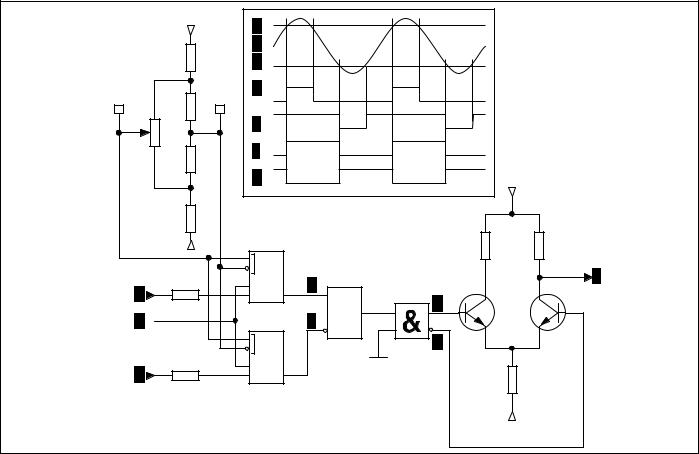
Comparator Stage
The comparator stage converts the analog signal from the impedance converter stage to a square wave. This circuit consists mainly of the high-speed integrated comparators U8A and U8B plus a separate trigger level circuit connected to the comparators at pins 9 and 13 via resistors R87 and R88.
The trigger level circuits, which are described later, generate a DC level in the range of approximately æ1.6 V. This covers a dynamic range of 6.4 V since the input signal is divided by a factor of 2 before it reaches the comparator.
The counter is provided with adjustable hysteresis, i.e., it is controllable via the front panel or GPIB. The circuitry for setting the hysteresis consists of the resistor network R91 to R96, supplied with +5 V and –5.2 V. It is connected to the latch enable inputs of the comparator, pin 5 and 7 for Comparator I and pin 17 and 15 for Comparator II.
The input signal is fed to both comparators, the outputs of which are used for setting/resetting the Flip-Flop U9.
Buffer Stage
Before the signal is fed further into the ASIC U29, it has to be level-shifted by a buffer stage. The negative ECL logic levels (~ –0.9 V to ~ –1.7 V) from U9 pins 17 and 18, are converted to a
single-ended signal with CMOS logic levels ( ~ 5 V to ~ 0 V).
The buffer is a differential amplifier consisting of the two transistors Q32 and Q33 whose bases are fed differentially from the two comparator outputs. Resistor R304 serves as a current generator that is switched alternately to the two collector resistors R296 and R297.
Trigger Level Circuits
The trigger level circuits generate the trigger voltage levels to the input comparators. The trigger level range is –3.2 V to + 3.2 V with a maximum resolution of 0.6 mV. The input amplifier attenuation is
|
+ 5 |
|
|
R92 |
|
TP27 |
R93 |
TP26 |
|
|
|
|
R91 |
|
|
R94 |
|
|
R96 |
|
|
- 5.2 |
|
T rig ger Level I |
R87 |
B |
Input si gnal A 
R88
Tri gger Level II |
C |
B
A
C
D
E
F
G |
|
|
|
|
+5 |
|
U8A |
|
|
|
R296 |
R297 |
|
|
|
|
|
|
|
|
|
|
|
|
|
F |
T o |
+ |
D |
U9 |
|
Q32 |
C ou nter |
|
|
U9 |
Q33 |
cir cu its |
|||
- |
|
F lip - |
||||
|
F |
|||||
|
|
|
|
|
|
|
U8B |
E |
F lo p |
|
|
|
|
|
|
|
|
G |
|
|
+ |
|
|
|
R304 |
|
|
- |
|
|
|
|
||
|
|
|
|
|
- 5.2 |
|
Fig. 4-8 Comparator flip-flop and buffer stages.
Hardware Functional Description 4-7
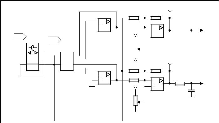
approximately 2 times. The trigger level circuits generate a DC level that has the same attenuation. This means that the output of this circuit has a range of –1.6 V to +1.6 V with a resolution of maximum 0.3 mV. A dual 8-bit DAC is used. The DACs only generate voltages between 0 and +1.6 V, but by using a X2 amplifier and an offset shift of 50%, the voltage range of –1.6 V to +1.6 V is achieved. The supply voltages to the trigger level circuits are filtered by R and C to prevent noise originating in the digital circuitry from influencing the trigger levels. The ground plane under the trigger level circuits is separated from the rest of the ground plane, and the planes are connected only at the front of the counter.
The trigger level circuits consist of the following:
–Resistor network R57 to R68 for generating the reference voltages 0.04 V, 0.22 V, 0.59 V, and 1.6 V.
–Three multiplexers (U3) to select one of the levels. With this arrangement there is a total trigger level range of
–1.6 V to +1.6 V.
–A double DAC (U4).
–Two current-to-voltage converters U6. These circuits convert the current at the IOUT pins of the DACs to a voltage. This signal has a range of 0 V to approximately 1.6 V.
–Two amplifiers, U7, with an amplification of X2, to generate a signal with a range of 0 V to 3.2 V. Resistors R69 and R70 set the reference voltage to the amplifier to get the 50 % offset shift. To get exact voltages, 0.5 % precision resistors are used: R73-R75, R78-R79 and R80-R82, R85-R86.
–The zero adjust of the trigger levels is done with trimmer potentiometers R69 and R70 connected to the amplifiers in U7.
–Two low-pass filters R87-C29 and R88-C30.
Tr ig ger l ev el C omp I
U6 |
R73-R74 |
R78-R79 |
|
|
|
|
R75 |
U7 |
|
|
|
|
U3 |
|
|
|
|
|
|
|
|
|
|
|
|
|
|
|
|
|
|
|
|
|
|
|
|
|
|
|
R87 C om par ator I |
||||||||||||
|
|
|
|
|
|
|
|
|
|
|
|
U4 |
|
|
|
|
|
|
|
|
|
|
|
|
|
|
|
|
|
|
|
|
|
|
|
|
|
|
|
|
|
|
|
|
A D0-A D2 |
|
|
|
|
|
|
|
|
|
|
|
|
|
|
|
|
|
|
|
+ 5 |
|
|
|
|
|
|
|
|
|
|
|
|
|
|||||||||||
|
|
|
|
|
|
|
|
|
|
|
|
|
|
|
|
|
|
|
|
|
|
|
|
|
|
|
|
|
|
|
|
|||||||||||||
|
|
|
|
|
|
|
|
|
|
|
|
|
|
|
|
|
|
|
|
|
|
|
|
|
|
|
|
|
|
|
|
|||||||||||||
|
|
|
|
|
|
|
|
D0D7 |
|
|
|
|
|
|
|
|
|
|
|
|
|
C29 |
|
|
|
|
|
|||||||||||||||||
|
|
|
|
|
AD0- A D8 |
|
|
|
|
|
|
|
|
|
|
|
|
|
|
|
|
|
|
|
|
|
|
|
|
|
|
|
|
|||||||||||
1.6V |
|
|
|
|
|
|
|
+ DA CA |
|
|
|
|
|
|
|
|
|
|
|
|
R69 |
|
|
|
|
|
|
|
|
|
|
|
|
|
|
|
|
|
||||||
|
|
|
|
|
|
|
|
|
|
|
|
|
|
|
|
|
|
|
|
|
|
|
|
|
|
|
|
|
|
|
|
|
|
|
|
|
|
|
|
|
|
|
||
|
|
|
|
|
|
|
|
|
|
|
|
|
|
|
|
|
|
|
|
|
|
|
|
|
|
|
|
|
|
|
|
|
|
|
|
|
|
|
|
|
|
|
||
|
|
|
|
|
|
|
|
|
|
|
|
|
|
|
|
|
|
|
|
|
|
|
|
|
|
|
|
|
|
|
|
|
|
|
|
|
|
|
|
|
|
|
||
|
|
|
|
|
|
|
|
|
|
|
|
|
|
|
|
|
|
|
|
|
|
|
|
|
|
|
|
|
|
|
|
|
|
|
|
|
|
|
|
|
|
|
||
0 .59V |
V RE F R F B |
|
|
|
|
|
|
|
|
|
|
|
|
|
|
|
|
|
|
|
|
|
|
|
|
|
|
|
|
|
|
|||||||||||||
|
|
|
|
|
|
|
|
|
|
|
|
|
|
|
|
|
|
|
|
|
|
|
|
|
|
Tr ig ger l evel |
|
|
|
|
|
|
|
|
||||||||||
|
|
|
|
|
|
|
|
|
|
|
|
|
|
|
|
|
|
|
|
|
|
|
|
|
|
|
|
|
|
|
||||||||||||||
|
|
|
|
|
|
|
|
|
|
|
|
I OUT |
|
|
|
|
|
|
|
|
|
|
|
|
|
|
|
|
|
|
|
|
|
|
|
|
|
|||||||
|
|
|
|
|
|
|
|
|
|
|
|
|
|
|
|
|
|
|
|
|
|
|
|
|
|
|
|
|
||||||||||||||||
0 .22V |
|
|
|
|
|
|
|
|
|
|
|
|
|
|
|
- 5.2 |
|
|
|
Com p I I |
|
|
|
|
|
|
|
|
||||||||||||||||
0 .04V |
|
|
|
|
|
|
|
|
|
|
|
|
|
|
|
|
|
|
|
|
|
|
|
|
|
|
|
|
|
|
|
|||||||||||||
|
|
|
|
|
|
|
|
|
|
|
|
|
|
|
|
|
|
|
|
|
|
|
|
|
|
|
|
|
|
|
|
|
|
|||||||||||
V RE F R F B |
|
|
|
I OUT |
U6 |
R80-R81 |
R85-R86 |
|
|
|
|
|
|
R82 |
U7 |
|
|
|
R88 C omp ara to r II
+ 5
C30
R70
 - 5.2
- 5.2
Fig. 4-9 Trigger level circuits.
4-8 Hardware Functional Description

Power Supply
General survey
The power supply generates four regulated DC supply voltages to the counter, as well as some other supply voltages for special purposes. The power supply block also contains the ON/STANDBY logic.
The main building block of the power supply is a primary switch mode power module (U39). The line power AC voltage (90 V to 265 V) is rectified to a DC voltage before it is fed to the power module.
After a line power filter in the power inlet, a fuse of 1.6 AT and an NTC resistor protect the power supply. The fuse F1 should only blow if a catastrophic error occurs on the primary side of the power supply. A short-circuit on the secondary side should not affect the primary side. To minimize the inrush current to the capacitors at the connection of the power cord, an NTC resistor (R148) is used. The resis-
tance is 15 when the resistor is cold but decreases to a few ohms as it is warmed up by the steady-state current.
The AC voltage is rectified in the bridge rectifier D9 and filtered in C64. C65 suppresses noise from D9. L6 and C82-C83 serve as a filter at the input of U39.
All inputs and outputs of the power module have HF chokes. The module is mounted with distance washers on the main board.
From the module there are three DC voltages outputs. One of those is regulated (+ 5 V) and the others are unregulated. These voltages will vary with input line voltage, the current at + 5 V, and at the unregulated voltages. The output marked +15 will be approximately +18 V, and the output marked –7 will be approximately –8 V. The outputs are filtered; HF is filtered by C70-C73, and LF is filtered by L7-L9 and C74-C76.
|
|
|
|
U40B |
|
|
|
K5 |
|
|
On |
|
|
|
|
|
Q14 |
|
|
|
+12 V* |
Stand by |
|
|
|
|
|
|
|
|
|
|
t |
|
|
|
U39 |
|
|
U43 |
|
|
|
MainsInle |
|
|
|
|
|
K5 |
|
|
||
Filter&Fuse |
|
|
PowerModule |
-7 |
|
|
|
|
||
|
|
|
U |
|
|
-5.2 V |
||||
|
|
|
|
|
|
|||||
D9 |
+5 |
|
|
|
|
|
||||
|
|
|
|
|
|
+5 V |
||||
|
|
|
|
|
|
|
||||
|
|
+15 |
R149-R155 |
J15 |
R130-R145 |
|
|
|||
|
|
|
Q5-Q6 |
|
||||||
|
|
|
|
|
||||||
|
|
|
|
|
|
|||||
|
|
|
|
|
|
|
|
|
|
+12 V |
U42 |
U |
|
|
|
|
U |
|
U |
+7 V |
|
|
|
|
|
|
|
|
|
|||
|
|
|
|
R156 |
|
|
U41 |
|
U21A&Q17 |
|
|
|
|
|
|
|
|
|
|
||
Fan |
|
|
|
|
|
*) for ON/STBY control & OCXO |
|
|||
PM6685R |
- |
J31 |
+ |
|
|
|
|
|
|
|
only |
|
|
|
|
|
|
|
|
|
|
|
|
|
|
|
|
|
|
|
|
|
Fig. 4-10 |
Power Supply. |
|
|
|
|
|
|
|
||
Hardware Functional Description 4-9
Function
The three DC voltages from the power module are used for generating the following four supply voltages in the counter:
+5 V
Regulated +5 V from the power module is used directly.
–5.2 V
–7 V is used, with regulator U43.
+12 V
+15 V is used, with regulator U41.
+7 V
Stabilized +12 V is used, with regulator U21A and Q17.
The following supply voltage is used for a special purpose:
+12 V*
This voltage comes directly from the +12 V regulator U41and will be present as soon as the power cord is connected, regardless of the position of the ON/STANDBY switch. It is used for the ON/STANDBY control logic and for supplying an optional OCXO in STANDBY to avoid the long warm-up time otherwise needed to obtain maximum accuracy.
At stand-by, the four main supply voltages are switched off, but as described above, some parts of the instrument should not be diconnected. Therefore the power module will never be switched off. The PM6685 has consequently only a secondary power switch.
A relay (K5) disconnects the load on the +5 V and –5.2 V at stand-by. Because the power module must always have a load on the regulated voltage, seven bleeder resistors R149-R155 are always connected to +5 V via J15. At stand-by the counter only needs +15 V, so a dummy load consisting of R130-R145 is connected to the power module by means of the relay K5 in order to stabilize the operation of the switchmode converter.
+5 V controls the switching on/off of +12 V and +7 V. When +5 V is on, Q6 and Q5 will conduct, i.e. +12 V will be on. If there is no +5 V, Q6 and Q5 will be off, thus blocking the +12 V.
The ON/STANDBY logic controls relay K5, which operates as described above. It is also possible to open the relay by changing the position of J16.
The ON/STANDBY logic consists of the RS (set-reset) flip-flop U40B that is controlled by the ON/STANDBY button on the front panel. Pressing STANDBY will apply a high voltage (+12 V) to the set input. The inverting output of the flip-flop will be low, disconnecting K5 via Q14. Pressing ON will give a high voltage (+12 V) on the reset input. The inverting output of the flip-flop will be high, engaging K5. Inserting the power cord into the power inlet will cause a pulse on the reset input, via C35. The microcomputer can disable the ON/STAND-BY button via Q12 and Q7. This is done in remote mode and during RAM-testing. A high level on the base of Q12 enables STAND-BY, a low level disables it.
The STAND-BY indicator on the front panel is controlled by the +5 V via Q16. +5 V off lights the STAND-BY LED that is fed by the uninterruptible +12 V*.
+5 V also indirectly controls the fan in the PM6685R. It is a 12 V DC fan that operates only if +12 V is on. An NTC resistor, serving as a
temperature sensor, controls the speed by applying a variable reference voltage to the fan voltage regulator U42.
Counter ASIC
The main part of the counting logic is integrated in a CMOS ASIC specially designed for the Fluke MultiFunction Counter series. There are also analog blocks included in the 100 pin QPF package.
MUX
The MUX block is a switchboard for incoming and internal signals involved in the measuring process. Some signals are divided by 2 to make it possible to measure higher frequencies. The trigger slope is controlled by the MUX block as well. A trigger edge detector senses the presence or absence of comparator pulses and controls the trigger level DAC’s in the TLDAC block. These functional units form an essential part of the Auto Trigger System.
OSC
The oscillator block generates, selects, and distributes the reference clock for the circuit. The active semiconductors of the standard oscillator are included in this block. The crystal is connected to pins X1 and X2. A TCXO or OCXO is connected to X2 only. An external reference clock is connected to EXTREF. The PWM signal generated at OTRIM controls the frequency of the reference oscillator after external integration.
PG
A built-in pulse generator having the 10 MHz clock as a reference can generate pulses with controllable duration and repetition rate at the OUTPUT connector. The level is fixed TTL.
RTC
A real time clock not used at present.
TLDAC
This block contains two 10-bit DAC’s generating the trigger levels for the input comparators, VOUTA for channel A and VOUTB for channel B. An external reference voltage is connected to V+REFA and V+REFB.
HO
The Hold Off block can manipulate the internal measuring signal X in several ways. One operating mode simulates a low pass filter (normal hold off), another mode is used in burst measurements.
The following blocks (SYNC, STST, CNTS and MCTRL) form the actual measuring logic in the ASIC. Three types of measurements can be made in this MEAS block:
Continuous measurements (frequency, ratio and period average). Not used at present.
Controlled measurements (time interval, period single, pulse width, frequency, totalize gated, totalize start-stop, and ratio).
Totalize manual.
SYNC
The SYNC block synchronizes the actual measurement with certain internal or external events like measuring time and arming signals.
STST
The start and/or the stop of the measurements are controlled by this block. External events can be used to define the exact moments.
4-10 Hardware Functional Description

A2 |
|
|
|
|
|
|
MUX |
|
|
||||||||
|
|
|
|
|
|
|
|
|
|
|
|||||||
A |
|
|
|
|
|
|
|
|
X |
|
|
||||||
|
|
|
|
|
|
|
|
||||||||||
SR |
|
|
|
|
|
|
|
|
Y |
|
|
||||||
|
|
|
|
|
|
|
|
||||||||||
B |
|
|
|
|
|
|
|
HODLYX |
|
|
|||||||
|
|
|
|
|
|
|
|
|
|||||||||
B2 |
|
|
|
|
|
|
|
|
|
|
|
|
|
||||
|
|
|
|
|
|
|
|
|
|
|
|
||||||
EXTC |
|
|
|
|
|
|
|
|
|
|
HODLYY |
|
|
||||
|
|
|
|
|
|
|
|
|
|
|
|||||||
P |
|
|
|
|
|
|
|
|
|
|
|
||||||
|
|
|
|
|
|
|
|
|
|
|
|||||||
BURST |
|
|
|
|
|
|
|
|
|
|
|
||||||
|
|
|
|
|
|
|
|
|
|
|
|||||||
TRA |
|
|
|
|
|
|
|
CLOCK |
|
|
|||||||
|
|
|
|
|
|
|
|
||||||||||
TRB |
|
|
|
|
|
|
|
S TAARM |
|
|
|||||||
|
|
|
|
|
|
|
|
|
|||||||||
V CCO |
|
|
|
|
|
|
|
|
|
|
|
|
|
||||
|
|
|
|
|
|
|
|
|
|
|
|
||||||
GNDD1 |
|
|
|
|
|
|
|
|
|
STOARM |
|
|
|||||
|
|
|
|
|
|
|
|
|
|
||||||||
GNDD2 |
|
|
|
|
|
|
|
|
|
STADLY |
|
|
|||||
|
|
|
|
|
|
|
|
|
|
||||||||
GNDD3 |
|
|
|
|
|
|
|
|
|
STODLY |
|
|
|||||
|
|
|
|
|
|
|
|
|
|
||||||||
GNDD4 |
|
|
|
|
|
|
TIME |
|
|
|
|
||||||
|
|
|
|
|
|
|
|
|
|
||||||||
|
|
|
|
|
|
|
|
|
|
|
|
|
|
|
|
|
|
|
|
|
|
|
|
|
|
|
|
|
|
|
M RE F |
|
|
|
|
|
|
|
|
|
|
|
|
|
|
|
|
|
F RE QC |
|
P CL |
|
|
|
|
|
|
|
|
|
|
|
|
|
|
|
M CLK |
|
|
|
|
GET |
|
|
|
|
|
P GARM |
PGTRIG |
|
|
||||||||
|
|
|
|
|
|
|
|
|
|
||||||||
|
|
|
|
|
|
|
|
|
|
||||||||
|
|
|
|
|
|
|
|
|
|
|
|
|
|
|
|
|
|
|
|
|
|
|
|
|
|
|
|
|
|
|
|
|
|
|
|
|
|
|
|
|
|
|
|
|
|
|
|
|
|
|
|
|
|
|
|
|
|
|
|
|
|
|
|
|
|
|
|
|
|
|
|
|
|
|
|
|
|
|
|
|
|
|
|
|
|
|
|
|
|
|
|
|
|
|
|
|
|
|
|
|
|
|
|
|
|
|
|
X1 |
|
|
|
|
|
|
|
|
|
|
|
|
OSC |
|
TIME |
|
|
|
|
|
|
|
|
|
|
|
|
|
|
|
|||||
X2 |
|
|
|
|
|
|
|
|
MREF |
|
|
||||||
|
|
|
|
|
|
|
|
|
|||||||||
V+REFO |
|
|
|
|
|
|
|
FRE QC |
|
|
|||||||
|
|
|
|
|
|
|
|
||||||||||
OTRIM |
|
|
|
|
|
|
|
|
MCLK |
|
|
||||||
|
|
|
|
|
|
|
|
||||||||||
V-REFO |
|
|
|
|
|
|
|
|
|
|
|
||||||
|
|
|
|
|
|
|
|
|
|
|
|||||||
E XTREF |
|
|
|
|
|
|
|
|
|
|
|
||||||
|
|
|
|
|
|
|
|
|
|
|
|||||||
MTCXO |
|
|
|
|
|
|
|
|
|
|
|
||||||
|
|
|
|
|
|
|
|
|
|
|
|||||||
INTREF |
|
|
|
|
|
|
|
|
|
|
|
||||||
|
|
|
|
|
|
|
|
|
|
|
|||||||
OUTMUX |
|
|
|
|
|
|
|
PGREF |
|
|
|||||||
|
|
|
|
|
|
|
|
||||||||||
MPCLK |
|
|
|
|
|
|
|
|
|
|
|
||||||
|
|
|
|
|
|
|
|
|
|
|
|||||||
P H1 |
|
|
|
|
|
|
|
|
|
|
|
||||||
|
|
|
|
|
|
|
|
|
|
|
|||||||
P H2 |
|
|
|
|
|
|
|
|
|
|
|
||||||
|
|
|
|
|
|
|
|
|
|
|
|||||||
V CCB |
|
|
|
|
|
|
|
|
|
|
|
||||||
|
|
|
|
|
|
|
|
|
|
|
|||||||
GNDB |
|
|
|
|
|
|
|
|
|
|
|
||||||
|
|
|
|
|
|
|
|
|
|
|
|||||||
VCCC |
|
|
|
|
|
|
|
|
|
|
|
||||||
|
|
|
|
|
|
|
|
|
|
|
|||||||
GNDC |
|
|
|
|
|
|
RTC |
|
|
|
|
||||||
|
|
|
|
|
|
|
|
|
|
||||||||
GNDA |
|
|
|
|
|
|
|
|
|
|
|||||||
|
|
+5 |
|
|
|
|
|
|
|||||||||
|
|
|
|
|
P GOUT |
|
|
|
|
||||||||
V CCA |
|
|
|
|
|
|
|
|
|||||||||
VCCX |
|
|
+5 |
|
|
|
|
|
|
|
|||||||
|
|
|
|
|
|
|
|
|
|||||||||
|
|
|
|
|
|
|
|
|
|
|
|
|
|
|
|
|
|
Fig. 4-11 Counter ASIC, block diagram.
PG
PGREF
|
|
|
|
|
|
|
|
|
|
|
|
|
|
|
|
RE SET |
|
|||
HO |
|
|
|
|
|
|
SYNC |
|
|
|
|
CNTS |
||||||||
X |
X H |
|
|
|
|
X H |
|
R1 |
|
|
|
R1 |
|
|
|
|
|
|
|
CY 1 |
Y |
Y H |
|
|
|
|
Y H |
|
R2 |
|
|
|
R2 |
|
|
|
|
|
|
|
CY 2 |
|
|
|
|
|
|
|
|
|
|
|
|
|
|
|
||||||
|
|
|
|
|
|
|
|
L1 |
|
|
|
L1 |
|
|
|
|
|
|
|
|
|
|
|
|
|
|
|
|
|
|
|
|
|
|
|
|
|
|
|
||
HODLYX |
HOS X |
|
|
|
|
|
|
L2 |
|
|
|
L2 |
INTB |
|
|
|
|
|
|
|
|
|
|
|
|
|
|
|
|
|
|
|
|
|
|
||||||
HODLYY |
HOS Y |
|
|
|
|
|
|
|
|
|
|
|
|
|
|
|
|
|||
|
|
|
|
|
|
|
|
|
|
|
||||||||||
|
|
|
|
|
|
|
|
|
|
|
|
|
INTA |
|
|
|
|
|||
|
|
|
|
|
|
|
|
|
|
|
|
|
|
|
|
|
SB |
|
|
|
|
|
|
|
|
CLOCK |
TEOGA |
|
|
|
|
|
|
|
|
|
|
|
SA |
|
|
|
|
|
|
|
|
|
|
|
|
|
|
NAF NBF |
NCF |
NDF OKA OKB COK OKD |
|
|
|
|
|||||
|
|
|
|
ST OP |
TOTSTA |
|
|
|
|
|
|
|
|
||||||||
|
|
|
|
ST ART |
|
|
STA |
|
|
|
|
|
|
|
|
|
|
|
|
|
|
|
|
|
|
|
|
|
|
|
|
|
I I I I |
|
|
|
|
|
|
|
|
||
|
|
|
|
HOS X |
|
S TOP |
|
|
|
|
|
|
|
|
|
|
|
Inter- |
VCCG |
||
|
|
|
|
HOS Y |
|
START |
|
|
|
|
|
|
|
|
|
|
polator |
GNDG |
|||
|
|
|
|
STA ARM |
|
|
|
|
|
|
|
|
|
|
|
|
VREFA D |
||||
|
|
|
|
|
|
|
|
|
|
|
|
|
|
|
|
|
|
|
|||
|
|
|
|
STOA RM |
|
|
|
|
|
|
|
|
|
|
|
|
|
|
|
IRES |
|
|
|
|
|
STA DLY |
|
|
|
|
|
|
|
|
|
|
|
|
|
|
|
INTP1 |
|
|
|
|
|
STODLY |
|
|
|
|
|
|
|
|
|
|
|
|
CLOCK |
|
INTP2 |
||
|
|
|
|
GET |
|
|
|
|
|
|
|
|
|
|
|
|
|
FNa |
FNb OKa |
OKb |
INTS1 |
|
|
|
|
TOTSTA |
STST |
|
|
|
|
|
|
|
|
|
|
INTS2 |
|||||
|
|
|
|
STA |
|
|
|
|
|
|
|
|
|
|
|
I I |
|
|
|||
|
|
|
|
|
|
|
|
|
|
|
P CL |
|
|
|
MCTRL |
|
|
FIN |
|||
|
|
|
|
|
|
|
|
|
|
|
|
DMAR |
|
DMABR |
|
|
|
|
MTIM E |
||
|
|
|
|
|
|
|
|
|
|
|
OK |
FIN1 |
|
|
|
TLDAC |
VOUTA |
||||
|
|
|
|
|
|
|
|
|
|
|
|
|
|
|
|
|
|
V+REFA |
|||
PGTRIG |
RTC |
|
|
|
|
|
|
|
|
|
|
|
|
|
|
|
|
|
V-RE FA |
||
|
|
|
|
|
|
|
|
|
|
|
|
|
|
|
|
|
|
|
|||
GOUTP |
|
RTC |
|
|
|
|
|
|
|
|
|
|
|
|
|
|
|
|
|
|
V+REFB |
|
|
|
|
|
|
|
|
|
|
|
|
|
|
|
|
|
|
|
VOUTB |
||
|
|
|
|
|
|
|
|
|
|
|
|
|
|
|
|
|
|
|
|
|
|
|
PGA RM |
|
|
|
|
|
|
|
|
|
|
|
|
|
|
|
|
|
|
|
V-RE FB |
|
|
|
|
|
|
|
|
|
|
|
|
|
|
|
|
|
|
|
|
|
VCCE |
|
|
|
|
|
|
|
|
|
|
|
|
|
|
|
|
|
|
|
|
|
GNDE |
|
|
|
|
|
|
CS |
RS |
SS |
MCLK |
|
|
|
|
|
|
|
|
|
|
||
|
|
|
|
|
|
|
|
|
|
|
|
MPI |
|
|
|
|
|
|
|
VCCF |
|
|
|
|
|
|
|
|
|
|
|
|
|
|
|
|
|
|
|
|
GNDF |
||
|
PG |
RTCX1 |
RTCX2 ALARMN |
VBAT |
|
AD0-AD15 |
ALE RDN |
WRHN WRLN CS |
A16 |
A17 |
A18 |
A19 HOLDN |
HLDAN |
QDMAN |
INT |
S1N |
S2N S3N |
S4N S5N |
C1 C2 |
C3 C4 |
|
CNTS
Two 32-bit binary counters count external events or keep track of the time.
They are calibrated over the possible error pulse range to allow for any aberrations from the theoretical linear behavior.
Interpolator
This block is not used at present.
MCTRL
The different events in the measurement cycle of the ASIC are timed by this block.
MPI
This is the microprocessor interface block. The bus width is 16 bits, AD0 to AD15. Interrupts to the microprocessor are generated at INT.
GET
The GET signal from an optional GPIB interface can control the start of a measurement.
External Interpolator
The X-POLATOR unit is connected directly to the internal interpolator in the ASIC. It is used for increasing the time resolution beyond the limits set by the reference clock period of 100 ns. An error pulse is generated in the SYNC block. Its width is determined by the difference between an external event on an input channel and the next clock pulse. This pulse controls a current generator charging a capacitor. When the pulse has expired the voltage across the capacitor is A/D converted and the value is added to the result. There are two interpolators, one for the start event and one for the stop event.
Oscillator Circuits
CPU Oscillator
The microcontroller U11 is clocked at 12 MHz. The crystal B1 is connected to the XTAL inputs of the microcontroller.
Reference Oscillators
A 10 MHz crystal oscillator is used as the reference for the measuring logic. If a stable external 10 MHz reference is available, it can be connected to REF IN on the rear panel and selected by means of the EXT REF button on the front panel.
In addition to the standard crystal oscillator there are two optional oven-controlled crystal oscillators (OCXO) to choose from.
Standard
The uncompensated standard oscillator consists of the crystal B2, C109, C113-C115, R209 and R211. C115 is used for manual adjustment of the frequency when the calibration tolerance has been exceeded. The active circuitry is built into the ASIC U29 and is accessible via the pins marked X1 and X2.
OCXO
If one of the OCXOs is mounted, the standard oscillator has to be inactivated by moving the jumpers J23 and J25 to their alternative position. These oscillators are connected to J24 and are self-contained
Hardware Functional Description 4-11

units with facilities for coarse and fine adjustment. They are fixed to the main PCB with two screws. The output signal is AC-coupled to the X2 pin on U29 via C107.
External
This input consists of an AC-coupled line receiver with Schmitt trigger function (U28) and is protected against excessive voltage excursions by a resistor-diode network. The output signal from U28 has CMOS logic levels and is connected to the EXTREF pin on the counter ASIC U29.
Logic
Microcomputer Circuits
Microcontroller
The microcomputer circuitry consists mainly of the microcontroller U11, an Intel 16-bit CMOS 80C196, RAM (U22A), and EPROM (U23A). The microcontroller is clocked at 12MHz. The data and address lines AD0 to AD15 are shared by means of multiplexing. Therefore the addresses are stored in the latches U16A and U17A. The ALE signal (Address Latch Enable) enables the latches.
UVEPROM
The main program is stored in U23A that is mounted in an IC socket, making it easy to update and customize the instrument firmware by changing the EPROM.
EEPROM
Front panel settings, GPIB address and certain other data that are not changed frequently, e.g. information in the Protected User Data Area, are stored in U12A which does not need battery backup.
Reset Circuit
A special reset circuit, the power supply supervisor U10, is included in the design. If the +5 V supply line becomes lower than 4.5 V, the reset output pin 5 goes low and the microcontroller will start over. The length of the reset pulse is set by C88; 2.2 µF gives a pulse of approximately 30 ms. U10 also controls the reset pulse during power-up so that the microcontroller will be initiated correctly.
Keyboard Scanning
Main Board |
|
U13A |
Keyboard & Display |
||
|
|
||||
|
|
|
|
Latch |
Board |
|
U11 |
|
|
|
|
|
|
|
AD0-AD7 |
|
H0-H3 |
|
CPU |
|
|
|
|
P1.0 |
P1.1 |
HS1.0 |
|
|
|
|
|
|
-AD7 |
U14A |
|
|
|
|
Latch |
|
|
|
|
|
AD0 |
|
|
|
|
|
|
|
|
|
|
|
|
|
V0-V7 |
|
|
|
|
|
LOCAL/PRESET |
|
|
|
|
|
SCL |
|
|
|
|
|
SDA |
Fig. 4-13 Keyboard scanning.
The keyboard scanning is done in two modes. The first mode is active as long as no button has been detected as depressed. Then all outputs of U13A are set high, and the latch U14A is read. If no button has been depressed, all outputs are low. This check is done at every timer interrupt in the microcontroller, every 25 ms. If a button is depressed, one of the output bits is high. When this event is detected, mode two is entered. The outputs of U13A must be set high one after the other to find the specific button. When found, only this button will be checked, so other simultaneously depressed buttons will not be recognized. The depressed button must stay down for several timer interrupts before action is taken. After the button has been recognized, the timer interrupt SW will be waiting for the button to be released. The button must be released for several timer interrupts before the keyboard scanning returns to mode 1. Then the search for other activated buttons can be resumed.
The following three buttons are not scanned in this way:
–The ON button is connected to the ON/STANDBY logic in the power supply.
|
CPU |
Latch |
Counter |
|
|
ASIC |
|
||
|
|
|
|
|
|
|
Address Bus |
LCD |
LCD |
Key- |
|
|
Drivers |
|
Latch |
|
|
||
|
|
|
||
board |
Address & Data Bus |
|
|
|
|
|
|
||
|
|
I2C Bus |
|
|
rd |
|
|
|
|
GPIB |
|
EE |
|
|
|
PROM |
|
|
|
|
|
|
|
|
Fig. 4-12 Microcomputer circuits, block diagram. |
|
|
||
4-12 Hardware Functional Description

–The STAND-BY button is connected to the ON/STANDBY logic in the power supply.
–The LOCAL/PRESET button is connected directly to input pin 24 on the microcontroller U11. Pressing this button sends an interrupt to a special handler in the SW.
Rear Panel Unit
The rear panel contains the following connectors
INPUTS:
–External reference input D - REF IN (BNC)
–External arming input E - EXT ARM (BNC)
–Power supply inlet including EMI filter OUTPUTS:
–Internal reference output G - 10 MHz OUT (BNC)
If a GPIB interface is installed in the device, it is mounted on the rear panel and connected to the main board with a flat cable.
Besides the normal standard GPIB connector, this optional unit also has a BNC connector capable of outputting an analog representation of any three consecutive digits on the display.
There is also a 6 SPST DIP switch on this unit for setting the default
GPIB address.
|
|
|
|
|
|
|
90V-265V |
|
|
ON |
16 8 |
4 2 1 |
I E E E 488/ IE C 625 |
INT |
ER F ACE |
|
|
|
|
OF F |
A DDRE S S |
S H 1, AH1, T 5, L4, |
SR1, |
|
|
|
|||
A NA L OG OU T |
|
|
R L1, D C1, DT 1, E 2 |
-I NT |
-S T B Y |
|
|
||
|
|
|
|
|
|
P RI MA RY F US E |
I N S ID E |
||
|
|
|
|
|
|
B AT T E RY |
|||
P M962 1 |
P M9 62 6 |
|
P M9 628 / 85 |
|
1. 6AT |
|
|||
|
|
|
|
|
|
||||
P M962 3 |
P M9 67 8 |
|
P M9697 |
|
-EX T /L I NE |
|
|
||
|
|
EXT SUPPLY |
P OWE R |
|
|
||||
P M962 4 |
P M9 69 0 |
|
_ _ _ _ _ __ |
|
|
|
|||
|
|
12-24V DC |
|
|
|
||||
P M962 5 |
P M9 69 1 |
|
_ _ _ _ _ __ |
|
|
|
|
||
|
|
|
|
|
|
||||
|
|
10M Hz O UT |
RE F I N |
|
E XT AR M |
|
|
|
|
|
|
G |
|
D |
|
E |
|
|
|
Fig. 4-14 Rear panel.
Hardware Functional Description 4-13
 Loading...