


Model 3BX III
Three-Band
Dynamic-Range Expander with Impact Restoration
SERVICE MANUAL
All dbx products are manufactured under patents in the US and abroad, and on all dbx circuit designs dbx holds copyright in one or more of the following years: 1979-’85. “dbx” is a registered trademark of dbx, Newton, Mass. USA.
|
CONTENTS |
|
SPECIFICATIONS (performance minimums)............................ |
4 |
|
CIRCUIT DESCRIPTION.............................................. |
1 |
|
SCHEMATIC CONVENTIONS .......................................... |
1 |
|
SIGNAL PATH .................................................... |
1 |
|
CONTROL-VOLTAGE (CV) PATH ...................................... |
3 |
|
High-Band CV Path ............................................ |
5 |
|
Low-Band CV Path ............................................. |
7 |
|
Mid-Band CV Path ............................................. |
7 |
|
LED DISPLAYS ................................................... |
7 |
|
POWER SUPPLY and MUTE GENERATOR ................................ |
8 |
|
ALIGNMENT PROCEDURE.............................................. |
9 |
|
1. |
INSTRUMENTS REQUIRED ........................................ |
9 |
2. |
INSPECTION and WARMUP ....................................... |
9 |
3. |
POWER-SUPPLY TESTS .......................................... |
9 |
4. |
CONTROL-CIRCUITRY TESTS ..................................... |
9 |
5. |
VCA-SYMMETRY ADJUSTMENTS ................................... |
12 |
6. |
VCA-GAIN ADJUSTMENTS ....................................... |
13 |
7. |
PERFORMANCE TESTS .......................................... |
14 |
MODEL 3BX III PRINTED CIRCUIT BOARD ASSEMBLY.................... |
20 |
|
MODEL 3BX III MAIN ASSEMBLY..................................... |
25 |
|
SPECIFICATIONS (performance minimums)
|
To 50% increase, |
Expansion |
maximum 12 dB upward |
|
and 20 dB downward |
|
|
|
To +12 dB (upward |
Impact restoration |
only), program- |
|
dependent |
|
|
|
+0.5 dB 20 Hz – 20 kHz, |
Frequency response |
|
|
any setting |
|
|
Dynamic range |
107 dB |
|
|
Total harmonic distortion (THD), no |
|
|
0.15% |
expansion |
|
|
|
Intermodulation distortion (IMD) IHF or |
|
|
0.1%, any setting |
SMPTE |
|
|
|
Equivalent input noise |
–90 dBV |
|
|
|
Program-dependent, |
Attack rates |
|
|
optimized for each band |
|
|
|
Linear expander program |
|
-dependent, optimized; |
Release rates |
|
|
impact restorer |
|
adjustable |
|
|
Maximum input and output |
7 V |
|
|
Notes
1)Specifications are subject to change without notice.
2)All data are for 20 Hz-20 kHz unless otherwise specified; line inputs
are driven by a source impedance |
of 1 k-ohms and outputs are loaded by |
10 k-ohms in parallel with 1000 |
pF; all voltages are rms (root-mean- |
square). |
|
3)Dynamic range is defined as the difference between the maximum rms output signal and A-weighted noise. All noise figures are A-weighted.
4)Frequency response figures are for pink noise (or music).
5)SMPTE IMD is measured with 60 Hz and 7 kHz mixed 4:1; IHF (differencetone) IMD is measured with 19 kHz and 20 kHz mixed 1:1; output 1 V.
6)Inputs and outputs have identical polarity.
7)All dbx home products are designed to be used with components whose output impedance is less than or equal to 5 k-ohms. All units are designed to drive loads of at least 5 k-ohms in parallel with 1000 pF or less.
Model 3BX III Service Manual
CIRCUIT DESCRIPTION
SCHEMATIC CONVENTIONS
The 3BX III is a stereo unit, with two independent, identical signal paths. We will refer here to the left channel only (channel 1). Almost all of its components are identified by designations ending in L (e.g., C705L, R708L); the right channel’s component designations generally end in R; and components common to the channels generally end in numbers (e.g., C803, R801). Furthermore, components are coded according to their function within the system. The 700 series indicates the signal path or detector path (the detector section is common to both channels, so 700 components ending in a number are in this area, while those ending in L or R are in the signal path). The 800 series indicates the power supply. Finally, the L## series indicates the LED display (e.g., RL21, UL05).
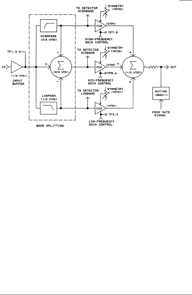
SIGNAL PATH
Refer to Fig. 1, a block diagram of the signal path (note that L, R suffixes are not shown and that test points [TPs] are for both channels, left first.) Audio input signals first are buffered by 1/2-U701L and its associated circuitry. The output of 1/2-U701L is TP1 (TP2, right channel). The signal there should be identical to that at the input except for a small attenuation (-0.83 dB) and a roll-off at 175 kHz.
Figure 1, Signal Path
– 1 –
Model 3BX III Service Manual
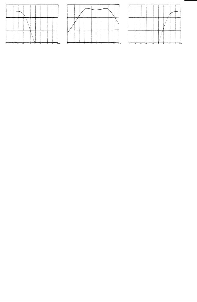
This signal is applied to a 4.21 kHz, two-pole high-pass filter (2/2- U702L), a 210 Hz, two-pole low-pass filter (1/2-U702L), and a summing stage (2/2-U701L). The summer subtracts the outputs of the high-pass and low-pass filters from the output of the buffer, forming a band-pass filter with cut-offs at about 4.21 kHz and 210 Hz. Its roll-off will be 6 dB/octave (with some peaking at each corner frequency), while that of the high-pass or low-pass filters is 12 dB/octave. Fig. 2 shows the frequency responses of these filters. Note that in their pass-bands the high-pass and low-pass filters are unity (0 dB) gain.
Figure 2, Low, Mid, and high Filters, 10 dB/division
The outputs of each filter are applied to the inputs of voltagecontrolled amplifiers (VCAs), one each for the low (U706L), mid (U705L), and high (U704L) ranges. The gain of each VCA is independently controlled by a voltage derived from the rms-level detector for each band and the front-panel control settings. This circuitry is described in the Control-Voltage Path section, next page.
The VCA’s gain in decibels is proportional to the voltage at pin 3 of each IC. Ideally the gain is 0 dB when the voltage is 0.00 mV; gain trims in the control-voltage (CV) path (see section 6 in the Alignment section) allow for a small adjustment. When pin 3 is positive, the gain in dB is negative (less than unity); when pin 3 is negative, the gain in dB is positive (greater than unity). Also under ideal conditions, variations in pin 3 voltage will not cause any variations in the dc level at the output of a VCA, but in the 3BX III, symmetry adjustments (VR701L for the low band, VR702L for the mid, VR703L for the high) are provided to compensate for non-ideal performance. (See the Alignment Procedure, sections 5.1 through 5.6, p.12 and following.) For a detailed explanation of this part, refer to the booklet on the VCA IC.
The outputs of all three VCAs are connected to a single summer stage, 2/2-U703 (in the right channel this stage is 1/2-U703). This op-amp converts the VCA-current output to a voltage signal and recombines the three bands into one. Note that the signal at pin 6 of U703 (pin 8 of the VCAs) is a current, not a voltage, which means that there won’t be very much voltage at pin 6 of U703 even if the VCA is working properly. By the way, a relatively large signal at this pin (more than 10-20 mV) usually indicates a fault with U703.
The output of 2/2-U703 goes through an RC-coupling stage (R731L, C776L, R732L) before connecting to the FET-based muting circuit (Q802 in the left channel, Q801 in the right channel). These FETs are turned on for a short time whenever power is applied or turned off, to attenuate the output during power-up and power-down transients.
– 2 –
Model 3BX III Service Manual
Finally, the signal passes to the switching circuitry. The switching allows the 3BX III signal path (a) to come either before or after a tape deck plugged into the tape jacks of the 3BX III, (b) to receive its signal from either the tape deck or the source, and (c) to bypass the circuitry.
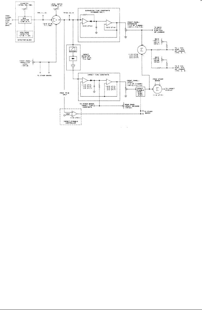
CONTROL-VOLTAGE (CV) PATH
The 3BX III has two main purposes: first, to make loud signals louder while making soft signals softer (upward and downward expansion), and second, to emphasize musical transients (impact restoration). The three rms detectors translate the signal level in each of the three bands into voltages (at dc or nearly so) that indicate how loud the input signal is in each of these bands. These voltages can then be processed and used to control the gain of the VCAs in the 3BX III to accomplish its two purposes. Choosing the correct time constants for the rms detectors in the first place is critical to doing this job right. Then the rmsdetector signals must be processed to find the transients and produce signals suitable for increasing the music’s impact. All of this detecting and processing takes place in the CV-path section of the 3BX III.
Refer to Fig. 3, a block diagram of the CV path. The audio signals at the outputs of each of the signal-path filters are connected to the inputs of three rms-level detectors, one for each band (U707 is the lowband detector, U708 the mid-band, U709 the high-band). For each band, the leftand right-channel signals are summed at pin 1 of the rmsdetector IC. For a detailed explanation of this part, refer to the booklet on the rms-detector IC.
Figure 3, Control-Voltage Path
– 3 –

Model 3BX III Service Manual
The output of these ICs (pin 7) is a dc voltage proportional to the dB signal level at the output of the filter that feeds them. TP9 is the low-band output, TP11 the mid-band, and TP13 the high-band. Table 1 shows the voltage and frequency required (simultaneously at the L- and R- channel inputs) to cause (ideally) 0.00 mV at pin 7 of each rms-detector IC. The exact calibration of these voltages is not critical, since adjustments are provided in the stage following the rms detector.
|
|
|
|
|
Approx. |
|
Input Voltage |
Input Frequency |
Rms IC |
Test Point |
|
|
|
|
|
|
|
|
Voltage |
|
|
|
|
|
|
|
|
227 mV |
100 Hz |
U707 |
TP9 |
0.00 |
mV |
|
|
|
|
|
|
|
|
88 |
mV |
1 kHz |
U708 |
TP11 |
0.00 |
mV |
|
|
|
|
|
|
|
69 |
mV |
10 kHz |
U709 |
TP13 |
0.00 |
mV |
|
|
|
|
|
|
|
TABLE 1
Input levels and frequencies (both channels driven) for 0.00 mV at the rms output
Along with the dc voltage is a small amount of ripple. Ideally, it will be at twice the frequency of the input, with no fundamental. Trim pots (VR704 in the low band. VR706 in the mid. and VR708 in the high) are provided to allow this waveform to be adjusted for perfect symmetry (see the Alignment Procedure, sections 4.1-4.3, p.9 and following). For larger input signals the rms-IC output is positive, and negative for smaller input signals; it varies by 6 mV for each decibel of input-level change.
The time-constant of the rms detector is dependent on the capacitance connected to pin 6. The larger the capacitor, the slower the time constant. The mid-band and high-band rms-detector ICs have small capacitors connected directly between pin 6 and ground (C731 in the mid band and C741 in the high band). Also connected to pin 6 is a larger capacitor (C720, C729, C740), which connects to an op-amp. This capacitor and the circuit to which it connects form a “nonlinear capacitor” with an equivalent “value” that changes with the signal conditions. If there are problems in verifying the expansion timing (see alignment procedure, section 7.2), check that this circuit is operating correctly by probing the output of the associated op-amp (pin 1 of U710 in the low band, of U711 in the mid band, and of U722 in the high band). The output of each op-amp should be a sinusoidal wave at twice the frequency of the input signal. See Table 2 for appropriate frequencies and levels.
|
|
|
|
|
Pin |
Approx |
|
Input Voltage |
Input Frequency |
Op-amp |
|
|
|
||
|
|
|
|
|
Number |
Voltage (p-p) |
|
|
|
|
|
|
|
||
1.0 |
v |
50 Hz |
U710 |
1 |
60 mV |
||
|
|
|
|
|
|
|
|
1.0 |
v |
100 |
Hz |
U711 |
1 |
540 |
mV |
|
|
|
|
|
|
|
|
1.0 |
v |
100 |
Hz |
U722 |
1 |
510 |
mV |
|
|
|
|
|
|
|
|
TABLE 2
Test conditions for the nonlinear-capacitor circuit
– 4 –

Model 3BX III Service Manual
The rms-detector outputs connect to inverting buffer stages (2/2-U710, 2/2-U711, and 2/2-U722) with gains of 9. At these buffers, individual dc voltages from trim pots VR705, VR707 and VR709 are added to the rmsdetector output voltages, and a single dc voltage from the TransitionLevel control (VR710 on the front panel) is added to all three stages. The trim pots allow the outputs of the rms detectors to be calibrated to specific references (see the Alignment Procedure, sections 4.1, 4.2 and 4.3), and the front-panel control allows the entire system’s unity-gain point (no upward or downward expansion) to be adjusted by the customer to match the levels in his or her stereo system.
TP10 is the low-band rms-buffer output, TP12 the mid-band, and TP14 the high-band. The CV path now splits in two, differently for the highand low-bands from the mid-band. First the high band…
High-Band CV Path
TP14 connects directly to the high-band-expansion control (VR715) on the front panel. This is one section of a three-gang pot (the other sections are labelled VR713 and VR711) which controls the amount of rms-detector signal that eventually reaches pin 3 of the high-band VCA IC. Setting the pot for more expansion causes more of this signal to be allowed through. At 50% expansion, a 100 mV change at the rms output (TP13) causes a negative 50 mV change at pin 3 of the VCA (TP7). When the signal at TP14 is positive, the gain of the high-band VCA will be either negative in dB or 0, depending on the position of the expansion control. When TP14 is negative, the gain will be positive or 0. The wiper of the expansion control connects to the positive input of a summer stage 2/2-U719) whose output is sent on to the VCA.
TP14 also connects to the impact detector (U720 and associated circuitry), which differentiates the rms-detector-output waveform and clips off the negative-going portions of it. Its output looks like a sharp positive-going spike every time a sudden increase in input-signal level takes place. This positive-going spike will cause the gain of the high-band VCA to increase (how much it increases depends on the setting of the Impact-Restoration control). Note that because the impact detector clips off the negative portions of the control signal, the impact restorer never causes negative gain (unlike the Expansion section). See Fig. 4, next page, for typical waveforms in the impactrestoration part of the CV path (note that column ‘a’ is low, ‘b’ is mid, ‘c’ is high). The output of the impact detector connects to a timeconstant circuit (1/2-U717, 2/2-U717), which stretches this spike out for a time determined by the setting of the rear Impact-Release-Rate control (VR723).
The output of the time-constant circuit is directly connected to the impact-level control (VR716) on the front panel. This, too, is one section of a three-gang pot (the other sections are labelled VR714 and VR712), and it controls the amount of impact-control signal that reaches pin 3 of the high-band VCA. The wiper of the pot connects to the impactdisable circuit (Q703, driven from 1/2-U721), which turns off the impactcontrol signal at low signal levels. This prevents record-surface noise and other small signals from being raised in volume by the impactrestoration circuitry.
– 5 –

Model 3BX III Service Manual
All photos:
All front controls @ maximum; Rear trim (Impact Release Rate) centred
a & b photos: |
c photos; |
300 Hz tone-burst @ 316 mV rms (447 mV peak), 128 cycles on, 172 cycles off, 0.2 s/div
3 kHz tone-burst @ 316 mV rms (447 mV peak), 128 cycles on, 172 cycles off, 20 ms/div
4.a.1 |
|
4.b.1 |
|
|
4.c.1 |
|
Top: Low-pass filter output, |
U702L, |
Top: Mid-band summer output, |
U701L, |
Top: High-pass |
filter output, |
U702L, |
pin 1, or U702R, pin 7, 0.2 V/div; |
pin 7, or U701R, pin 1, 0.5 V/div; |
pin 7, or U702R pin 1, 0.2 V/div; |
||||
Bottom: Low-band rms-detector |
output, |
Bottom: Mid-band rms-detector |
output, |
Bottom: High-band rms-detector |
output, |
|
U707, pin 7 (TP9), 0.1 V/div. |
U708, pin 7 (TP11), 50 mV/div. |
U709, pin 7 |
(TP13), 0.1 V/div. |
|||
|
4.a.2 |
|
4.b.2 |
|
4.c.2 |
|
Top: Low-band |
rms-buffer output, |
Top: Mid-band |
rms-buffer output, |
Top: High-band |
rms-buffer |
output, |
U710, pin 7 |
(TP10), 1 V/div; |
U711, pin 7 |
(TP12), 1 V/div; |
U722, pin 7 (TP14), 1 V/div; |
||
Bottom: Low-band impact-detector |
Bottom: Mid-band impact-detector |
Bottom: High-band impact-detector |
||||
output, U713, pin 5, 0.2 V/div. |
output, U714, pin 3, 0.5 V/div. |
output, U717, |
pin 5, 0.2 |
V/div. |
||
|
4.a.3 |
|
4.b.3 |
|
|
4.c.3 |
|
|
|
Top: Output, |
low-band |
impact time- |
Top: Output. mid-band |
impact time- |
Top: Output, high-band impact time- |
||||
constants, U713, pin |
1, 1 |
V/div; |
constants, U715, pin |
7, 1 |
V/div; |
constants, U717, pin 1, 0.5 |
V/div; |
||
Bottom: Low-band VCA control voltage, |
Bottom: Mid-band VCA control voltage, |
Bottom: High-band VCA |
control |
voltage, |
|||||
U706L or R, pin |
3 (TP3 or 4), |
0.1 V/div. |
U705L or R, pin 3 (TP5 or 6), |
0.1 V/div. |
U704L or R, pin 3 (TP7 |
or 8), 0.1 V/div. |
|||
|
Figure 4 |
|
4.a & b.4 |
|
4.c.4 |
|
||
Left or right output, 5 V/div |
|
Left or right output, 0.5 V/div |
– 6 –
Model 3BX III Service Manual
Finally, the output of the impact-disable circuit connects to the summer stage (2/2-U719) previously mentioned, where both the expansion and impact-restoration CVs are combined before being sent to the VCA. Trim pots (VR721 and VR722) are provided at the output of this summer to allow the CVs sent to each VCA (left and right channel) to be offset slightly, in order to account for differences in VCA-gain offsets (see Alignment Procedure, section 6, p.13).
Low-Band CV Path (see Fig. 4)
This path is nearly identical to the high-band, except that the timeconstants used throughout are generally much longer, as is appropriate for low frequencies. The signal at TP10 (the output of the buffer following the low-band rms output) splits into two paths: one to the expansion control (VR711) and one to the impact detector. The output of the impact detector goes through a circuit to lengthen the decay, and then to the impact-disable circuit. (The impact-disable controller is common to all three bands.) The impact-control signal and the expansioncontrol signals are combined in 1/2-U718 and then sent to the low-band VCAs. Trim pots VR717 and VR718 are provided to set the VCA gains precisely.
Mid-Band CV Path (again see Fig. 4)
This path also closely resembles the high-band, except for different time-constants (midway between the lowand high-band ones) and the addition of a mid-band expansion time-constant circuit. This circuit is placed between the output of the buffer following the mid-band rms detector (TP12) and the front panel expansion control (VR713). Its purpose is to prevent the mid-band CV from dropping too fast after an input signal goes away (toward lower signal level indication, which at this point is toward positive voltages). This circuit closely resembles the impact time-constant circuit; it performs a similar function but does not provide a user-adjustable release rate.
LED DISPLAYS
Refer to Fig. 5, a block diagram of a typical LED display. The control voltages from each of the three sections of the Impact-Restoration control are summed in 1/2-U719 to produce a signal representative of the average of the impact CVs.
This signal is sent to the LEDdisplay section. In addition, the CVs from each of the three sections of the Expansion-Level control (VR711, VR713, and VR715) are sent
(separately) there.
Figure 5, LED Display
– 7 –
Model 3BX III Service Manual
In the LED display, current sources (QL01 through QL08) of approximately 7 mA each provide constant currents to each series-connected string of six LEDs regardless of the number of LEDs on at any one time. The LM339 comparator sections (UL01 through UL12) have open collector outputs that shunt the LED supply currents to ground when they are “low” and allow the currents to pass into the LEDs when they are “high.” This turns off all the LEDs “below” the last comparator whose output is low. Any LEDs between the current source and the uppermost low comparator will be illuminated.
The comparators compare the CV signals with a set of predetermined voltages set by resistor strings across the supply voltage. For the red LEDs, the comparator goes high and an individual LED turns on when the CV negatively exceeds the fixed voltage at the comparator’s other input. For the yellow LEDs, the CV must positively exceed the fixed voltage to turn on an LED. Because of the series connection, if any one LED is open, all LEDs in that string will go out as soon as the comparator at the bad LED goes high. An open in a comparator output will cause its LED to light as soon as the one “above” it is lit; a short in a comparator output will prevent any LEDs from lighting “below” that comparator.
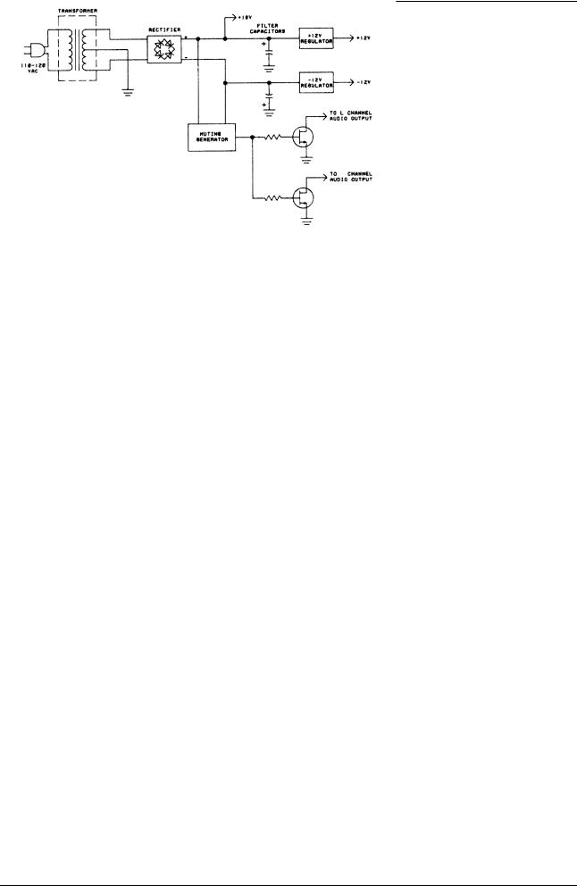
POWER SUPPLY and MUTE GENERATOR
Refer to Fig. 6, a block diagram of the power supply. The secondary of the power transformer produces approximately 37 Vac rms (the normal range is 31 to 43 V), which is full-wave rectified by the bridge rectifier (D801-D804) and smoothed by electrolytic capacitors (C801-C804) to produce approximately +18 Vdc (the normal range is 17 to 24 V). Threeterminal regulators reduce this voltage to a constant +12 Vdc, which is used to supply most of the circuitry. The unregulated +18 Vdc is used to supply current to the LED strings.
Figure 6, Power Supply
Also in the power-supply section is the muting generator (Q803, etc.). Refer to the main schematic for details. The output of this circuit (the collector of Q803) is normally -18 V. However, it produces a short positive pulse when power is first applied or removed. The pulse on turn-on lasts longer than the time required for the supplies to stabilize, and the pulse after turn-off lasts longer than the time required for the supplies to collapse. These pulses turn on the muting FETs (Q801 and Q802), shorting the audio output to ground during the On and Off transients.
– 8 –
 Loading...