

Page 1
®
HIGH FREQUENCY SECONDARY RECTIFIER
MAJOR PRODUCT CHARACTE RISTICS
STTH3003CW
I
F(AV)
V
RRM
2 x 15 A
300 V
Tj (max) 175 °C
(max) 1 V
V
F
trr (max) 40 ns
FEATURES AND BENE FITS
COMBINES HIGHEST RECOVERY AND
REVERSE VOLTAGE PERFORMANCE
ULTRA-FAST, SOFT AND NOISE-FREE
RECOVERY
DESCRIPTION
Dual center tap Fast Recovery Epitaxial Diodes
suited for Switch Mode Power Supply and high
frequency DC to DC converters.
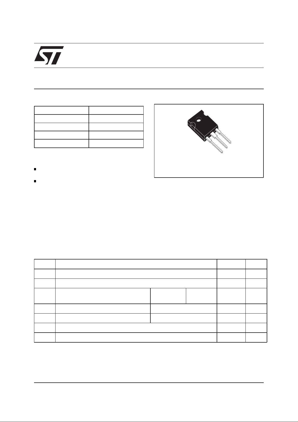
Packaged in TO-247 this device is intended for
secondary rectification.
ABSOLUTE RATINGS (limiting values, per diode)
A2
K
A1
TO-247
Symbol Parameter Value Unit
V
RRM
I
F(RMS)
I
F(AV)
I
FSM
I
RSM
T
stg
Tj
October 1999 - Ed: 5A
Repetitive peak reverse voltage
RMS forward current
Average forward current Tc = 135°C
Surge non repetitive forward current tp = 10 ms sinusoidal
Non repetitive peak reverse current tp = 20 µs square
Storage temperature range
Maximum operating junction temperature
δ = 0.5
Per diode
Per device
300 V
30 A
15
30
140 A
7A
-65 +175 °C
+175 ° C
A
1/5
Page 2

STTH3003CW
THERMA L RE SISTA NC ES
Symbol Parameter Value Unit
R
th (j-c)
Junction to case Per diode
Total
R
th (c)
Coupling
STATIC ELECTRICAL CHARACTERISTICS (per diode)
Symbol Parameter Tests conditions Min. Typ. Max. Unit
2.0 °C/W
1.05
0.1
*
I
R
V
F
Reverse leakage
current
**
Forward voltage drop I
V
= 300 V Tj = 25°C
R
Tj = 125°C
= 15 A Tj = 25°C
F
Tj = 125°C
40 400
0.85 1
40 µA
1.25 V
Puls e tes t : * tp = 5 m s, δ < 2 %
** tp = 380 µs, δ < 2%
To evaluate the maximum conduction losses use the following equation :
P = 0.75 x I
F(AV)
+ 0.017 I
F2(RMS)
RECOVERY CH ARACTE RIST ICS
Symbol Tests conditions Min. Typ. Max. Unit
trr
= 0.5 A Irr = 0.25 A IR = 1A Tj = 25°C
I
F
IF = 1 A dIF/dt = - 50 A/µ s VR = 30V
tfr
V
FP
I
= 15 A dIF/dt = 100 A/µs
F
V
= 1.1 x VF max.
FR
Tj = 25°C
30 ns
40
300 ns
3.5 V
2/5
S
factor
I
RM
Vcc = 200 V IF = 15 A
dI
/dt = 200A/µs
F
Tj = 125°C
0.3 -
8.5 A
Page 3

STTH3003CW
Fig. 1: Conduction losses versus average current
(per diode).
P1(W)
20
18
16
14
δ = 0.05
δ = 0.1
δ = 0.2
δ = 0.5
δ = 1
12
10
8
6
T
4
2
0
02468101214161820
IF(av) (A)
δ
=tp/T
tp
Fig. 3: Relative variation of thermal impedance
junction to case versus pulse duration.
Zth(j-c)/Rth(j-c)
1.0
0.8
δ = 0.5
0.6
δ = 0.2
0.4
δ = 0.1
0.2
Single pulse
tp(s)
0.0
1E-3 1E-2 1E-1 1E+0
δ
=tp/T
T
tp
Fig. 2: Forward voltage drop versus forward
current (maximum values, per diode).
IFM(A)
200
100
Tj=125°C
10
Tj=25°C
Tj=75°C
VFM(V)
1
0.50 0.75 1.00 1.25 1.50 1.75 2.00 2.25 2.50
Fig. 4: Peak reverse recovery current versus
dI
/dt (90% confidence, per diode).
F
IRM(A)
16
VR=200V
14
Tj=125°C
12
IF=IF(av)
10
8
6
4
2
0
0 50 100 150 200 250 300 350 400 450 500
dIF/dt(A/µs)
IF=2*IF(av)
IF=0.5*IF(av)
Fig. 5: Reverse recovery time ver sus dI
F
confidence, per diode).
trr(ns)
100
80
60
IF=2*IF(av)
40
20
IF=0.5*IF(av)
dIF/dt(A/µs)
0
0 50 100 150 200 250 300 350 400 450 500
VR=200V
Tj=125°C
IF=IF(av)
/dt (90%
Fig. 6: Softness factor versus dI
/dt (typical
F
values, per diode).
S factor
0.60
0.50
0.40
0.30
0.20
0.10
0.00
0 50 100 150 200 250 300 350 400 450 500
dIF/dt(A/µs)
VR=200V
Tj=125°C
3/5
Page 4

STTH3003CW
Fig. 7: Re lative variati on of dynamic par ameters
versus junction temperature (reference: Tj = 125°C).
2.6
2.4
2.2
2.0
1.8
1.6
1.4
1.2
1.0
0.8
0.6
0.4
0.2
0.0
25 50 75 100 125
Fig. 9: Forward recovery time versus dI
IRM
S factor
Tj(°C)
/dt (90%
F
confidence, per diode).
tfr(ns)
500
450
400
350
300
250
200
150
100
50
0
0 50 100 150 200 250 300 350 400 450 500
dIF/dt(A/µs)
VFR=1.1*VF max.
IF=IF(av)
Tj=125°C
Fig. 8: Transient peak forward voltage versus
dI
/dt (90% confidence, per diode).
F
VFP(V)
8
IF=IF(av)
7
Tj=125°C
6
5
4
3
2
1
0
0 50 100 150 200 250 300 350 400 450 500
dIF/dt(A/µs)
4/5
Page 5

PACKAGE MECHANICAL DAT A
TO-247
V
V
H
L5
L
F2
F4
L1
F3
L3
F1
V2
F(x3)
G
= =
Dia.
L4L2
D
ME
A
STTH3003CW
DIMENSIONS
REF.
A 4.85 5.15 0.191 0.203
D 2.20 2.60 0.086 0.102
E 0.40 0.80 0.015 0.031
F 1.00 1.40 0.039 0.055
F1 3.00 0.118
F2 2.00 0.078
F3 2.00 2.40 0.078 0.094
F4 3.00 3.40 0.118 0.133
G 10.90 0.429
H 15.45 15.75 0.608 0.620
L 19.85 20.15 0.781 0.793
L1 3.70 4.30 0.145 0.169
L2 18.50 0.728
L3 14.20 14.80 0.559 0.582
L4 34.60 1.362
L5 5.50 0.216
M 2.00 3.00 0.078 0.118
V5° 5°
V2 60° 60°
Dia. 3.55 3.65 0.139 0.143
Millimeters Inches
Min. Typ. Max. Min. Typ. Max.
Ordering code Marking Package Weight Base qty Delivery mode
STTH3003CW STTH3003CW TO-247 4.36g 30 Tube
Cooling method: by conduction (C)
Recommended torque value: 0.8 N.m.
Maximum torque value: 1.0 N.m.
Epoxy meets UL 94,V0
Information furnished is believed to be accurate and reliable. However, STMicroelectronics assumes no responsibility for the consequences of
use of such information nor for any infringement of patents or other rights of third parties which may result from its use. No license is granted by
implication or otherwi se un der any pat ent or patent rights of STMic roelec tronics. S pecifications ment ioned in t his publ ication are subject to
change without notice. This publication supersedes and replaces all information previously supplied.
STMicroelectronics products are not author i zed f or use as critical comp onents i n l i fe s upport devices or systems without express written approval of STMicroelectronics.
The ST logo is a registered trademark of STMicroe lectronics
© 1999 STMicroelectronics - Printed in Italy - All rights reser ved.
STMicroelectronics GROUP OF COMPANIES
Australia - Brazil - China - Finland - France - Germany - Hong Kong - India - Italy - Japan - Malaysia
Malta - Morocco - Singapore - Spain - Sweden - Switzerland - United Kingdom - U.S.A.
http://www.st.com
5/5
 Loading...