

A/D, D/C Converters for Image Signal Processing
MN657021F
Low Power 8-Bit, 3-Channel CMOS D/A Converter for Image Processing
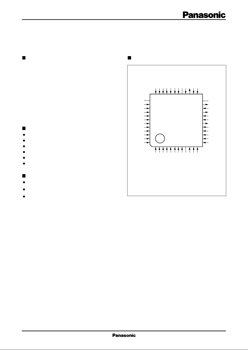
Pin Assignment Overview
The MN657021F is a high-speed 8-bit, 3-channel
CMOS digital-to-analog converter. (Two channels use
serial input.)
It uses both a matrix cell and weighted current technology to achieve both low power consumption and high
speed.
It provides independent output amplitude adjustment
for the Y (luminance) and C (chroma) synchronization
signals. The Y (luminance signal) can be superimposed
with an external SYNC signal.
Features
Maximum conversion rate: 27 MSPS (min.)
Linearity error: ±0.2 LSB (typ.)
Differential linearity error: ±0.2 LSB (typ.)
Power supply voltage: 3.15 ±0.3 V
Full scale current: 1.75 mA (typ.)
Power consumption: 54 mW (typ.) (f
=27 MHz)
CLK
N.C.
DC3
DC2
DC1
UVSEL
DV
DV
CLK
DY8
DY7
DY6
DY5
DC4
DC5
DC6
DC7
DC8
DVSSDVDDN.C.
3635343332313029282726
37
38
39
40
41
42
DD
43
SS
44
45
46
47
48
1234567891011
DY2
DY1
DD
DV
SYNC
DY4
DY3
SS
DV
AVSSV
N.C.
MSEL
REFC
DD
AV
REFC
I
COMPC
25
24
23
22
21
20
19
18
17
16
15
14
13
12
REFS
I
COMPS
N.C.
I
OV
AV
I
OU
AV
AV
I
OY
AV
V
I
REFY
COMPY
V
DD
SS
DD
SS
REFY
REFY
Applications
Digital television
Digital video equipment
Digital image processing equipment
(TOP VIEW)
TQFP048-P-0707
1
MN657021F A/D, D/C Converters for Image Signal Processing
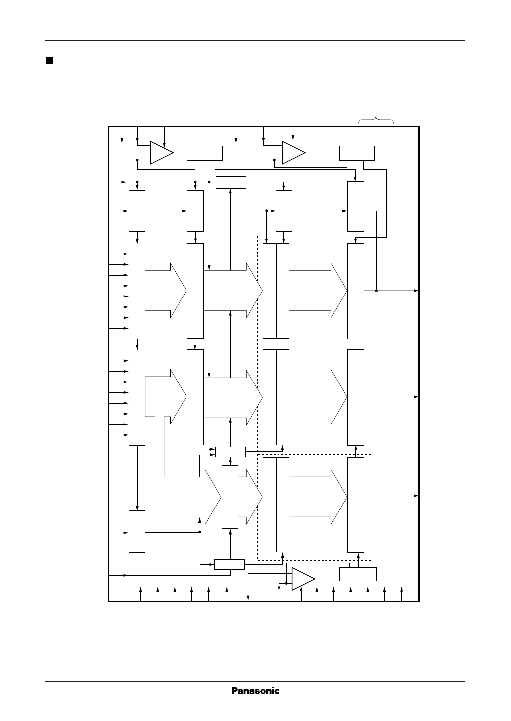
Block Diagram
CLK
SYNC
(MSB) DY1
DY2
DY3
DY4
DY5
DY6
DY7
(LSB) DY8
(MSB) DC1
DC2
DC3
DC4
DC5
DC6
DC7
(LSB) DC8
Current
Source
N.C.
372924
9
REFS
REFS
I
V
COMPS
12
13
11
+
–
Current
Source
44
15
Selector
REFY
I
REFY
V
16
COMPY
14
+
–
5
Latch
Latch
Latch
Current cellCurrent cellCurrent cellCurrent cell
4
3
2
1
48
Latch
47
Latch
Latch
18
I
OY
46
45
40
39
38
36
35
Latch
34
Latch
LatchLatch
21
I
OU
33
32
Selector
23
I
OV
UVSEL
MSEL
Selector
41
Latch
8
6
30
42
DDDVDDDVDD
DV
Selector
7
31
DVSSDVSSDV
43
SS
Decoder Decoder Decoder
+
–
27
REFC
V
26
25
10
REFC
I
COMPC
Current
Source
19
22
DD
AVDDAVDDAV
17
20
AVSSAVSSAV
28
SS
2
A/D, D/C Converters for Image Signal Processing MN657021F
Pin Descriptions
Pin No. Symbol Function Description
1 DY4 Y (luminance) digital input
2 DY3 Y (luminance) digital input
3 DY2 Y (luminance) digital input
4 DY1 Y (luminance) digital input (MSB)
5 SYNC SYNC signal judgment signal
6DVDDPower supply for digital circuits
7DVSSGround for digital circuits
8 MSEL Y, C/Y, R-Y, B-Y discrimination signal
9 N.C. No connection
10 AV
DD
11 COMPS Phase compensation
12 I
13 V
REFS
REFS
14 COMPY Phase compensation
15 I
16 V
17 AV
18 I
19 AV
20 AV
21 I
22 AV
23 I
REFY
REFY
SS
OY
DD
SS
OU
DD
OV
24 N.C. No connection
25 COMPC Phase compensation
26 I
27 V
28 AV
REFC
REFC
SS
29 N.C. No connection
30 DV
31 DV
DD
SS
32 DC8 C (chroma) digital input (LSB)
33 DC7 C (chroma) digital input
34 DC6 C (chroma) digital input
35 DC5 C (chroma) digital input
36 DC4 C (chroma) digital input
37 N.C. No connection
38 DC3 C (chroma) digital input
39 DC2 C (chroma) digital input
40 DC1 C (chroma) digital input (MSB)
41 UVSEL U/V signal discrimination for C (chroma) signal
42 DV
DD
Power supply for analog circuits
Full scale adjustment resistor
SYNC reference voltage input
Full scale adjustment resistor
Luminance reference voltage input
Ground for analog circuits
Y signal analog current output
Power supply for analog circuits
Ground for analog circuits
U signal analog current output
Ground for analog circuits
V signal analog current output
Full scale adjustment resistor
Chroma reference voltage input
Ground for analog circuits
Power supply for digital circuits
Ground for digital circuits
Power supply for digital circuits
3
MN657021F A/D, D/C Converters for Image Signal Processing
Pin Descriptions (continued)
Pin No. Symbol Function Description
43 DV
SS
44 CLK Sampling clock
45 DY8 Y (luminance) digital input (LSB)
46 DY7 Y (luminance) digital input
47 DY6 Y (luminance) digital input
48 DY5 Y (luminance) digital input
Absolute Maximum Ratings Ta=25˚C
Parameter Symbol Rating Unit
Power supply voltage for digital circuits DV
Power supply voltage for analog circuits AV
Input voltage V
Output voltage V
Operating ambient temperature T
Storage temperature T
Recommended Operating Conditions V
Parameter Symbol min typ max Unit
Power supply voltage V
Reference voltage V
Reference resistance R
External compensation capacitor C
Output load resistance R
Digital input "H" level V
voltage "L" level V
Clock "H" level pulse width t
Electrical Characteristics DV
Parameter Symbol Conditions min typ max Unit
Power supply current I
Resolution RES 8 bit
Linearity error E
Differential linearity error E
Full scale current I
Setup time t
Hold time t
Settling time t
Maximum conversion speed F
Analog output delay time t
Ground for digital circuits
COMPS, Y , C
"L" level pulse width t
=AVDD=3.0V, DVSS=AVSS=0V, Ta=25˚C
DD
F
DD
CLK
Output amplitude=0.7 V, 18 28 mA
R
OUT
VDD=3.0V , Y output amplitude=0.7V ±0.2 ±0.5 LSB
L
UV output amplitude=0.7V ±0.2 ±0.5 LSB
D
R
FS
ST
C(max.)
OUT
R
REFY
S
H
VDD=3.0V , Y output amplitude=0.7V , 25 37 ns
UV output amplitude=0.7V
R
OUT
VDD=3.0V , Y output amplitude=0.7V ,
d
UV output amplitude=0.7V
DD
DD
I
O
opr
stg
=AVDD=DVDD=3.0V, VSS=AVSS=DVSS=0V, Ta=25˚C
DD
DD
REFS/Y, C
REFS/Y, C
2.85 3.0 3.45 V
1.0 1.85/1.63 2.3 V
2.0/0.58 5.0/2.5 8.0/5.0 kΩ
0.33 1.0 3.3 µF
OUT
IH
IL
WH
WL
75 400 500 Ω
VDD × 0.75 V
V
16 ns
16 ns
=30MHz, MSEL="H",
=400Ω
=400Ω
=2.5kΩ, R
=400Ω, R
REFC
REF
=2.5kΩ
=2.5kΩ
SS
– 0.3 to +7.0 V
– 0.3 to +7.0 V
– 0.3 to DV
– 0.3 to AV
+0.3 V
DD
+0.3 V
DD
–20 to +70 ˚C
–55 to +125 ˚C
DD
VDD × 0.25 V
1.75 mA
12 ns
10 ns
27 MSPS
10 ns
V
4
A/D, D/C Converters for Image Signal Processing MN657021F
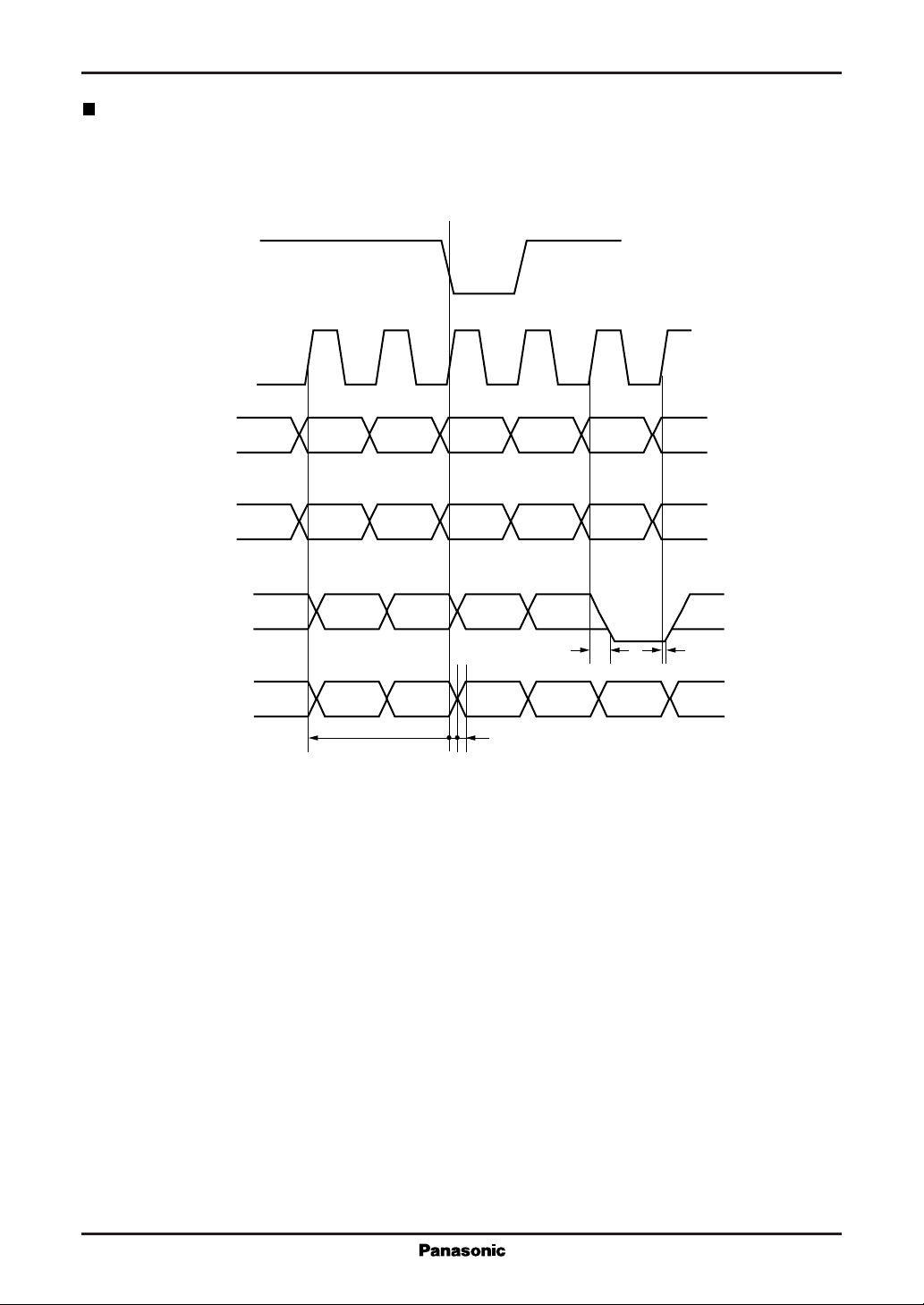
Timing Chart
M SELECT = "L," Y and U(C), 2-channel output
SYNC
CLK
DY1 to DY8
DC1 to DC8
I
OY
I
OU
Y-1
C-1
Y0
C0
Y-3
Y1
C1
Y2
C2
Y3
C3
Y-2 Y-1 Y-0 Y1
t
ds
Y4
C4
C-3 C-2 C-1 C-0 C1 C2 C3
Two clock cycles
t
t
d
st
tds: SYNC delay time
: Analog output delay time
t
d
t
: Settling time
st
Y5
C5
Y3
t
ds
5
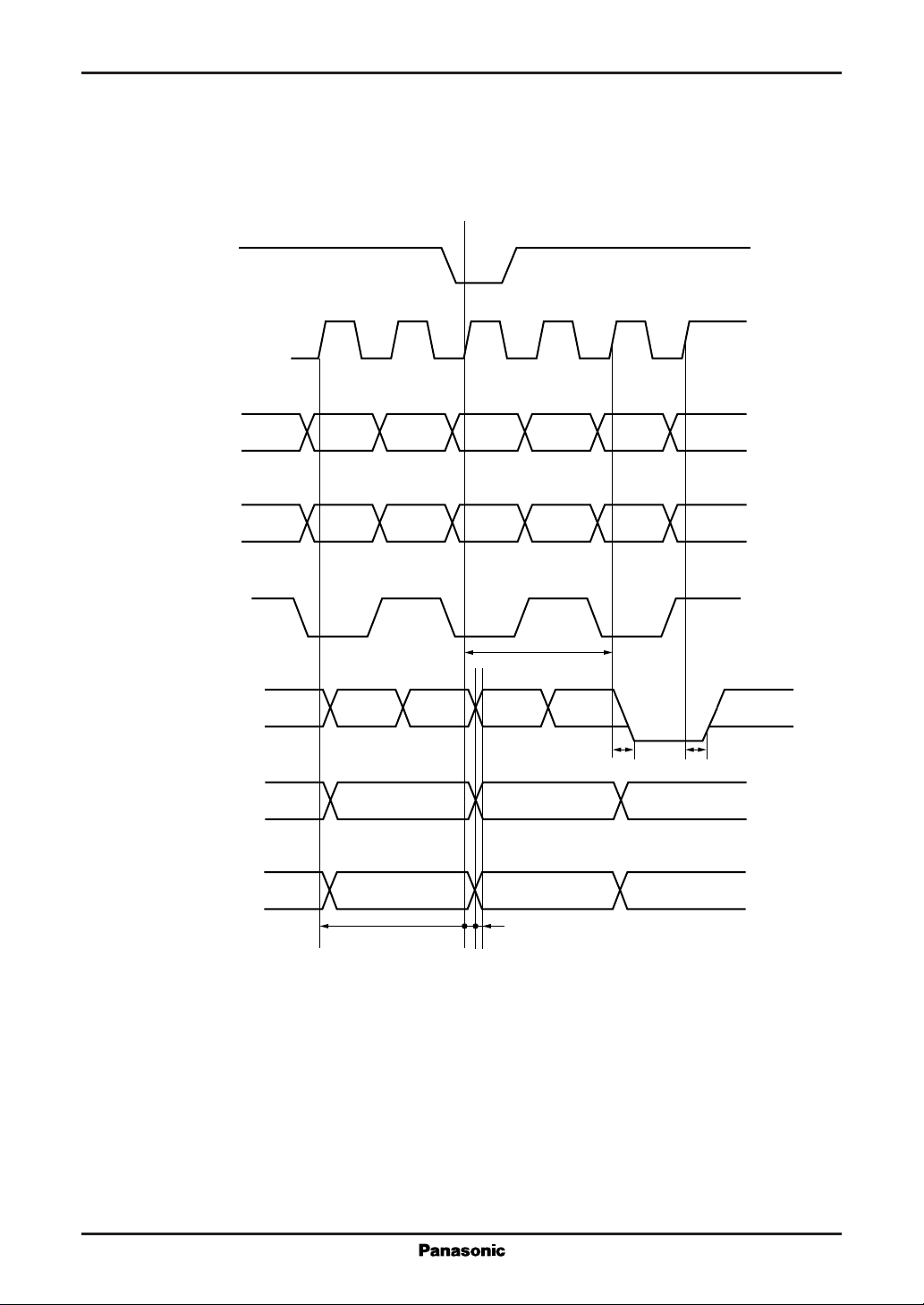
MN657021F A/D, D/C Converters for Image Signal Processing
M SELECT = "H," Y and U(C), 3-channel output
SYNC
CLK
DY1 to DY8
DC1 to DC8
UVSEL
I
OY
I
OU
I
OV
Y-1
Y-2
Y0 Y1 Y2 Y3 Y4 Y5
U0 U2 U4V0
V2 V4
Two clock cycles
Y-2
U-4
Y-1
Y0 Y1 Y3
t
ds
U-2 U0 U2
V-4 V-2 V0 V2
Two clock cycles
t
t
d
st
tds: SYNC delay time
: Analog output delay time
t
d
: Settling time
t
st
t
ds
6
A/D, D/C Converters for Image Signal Processing MN657021F
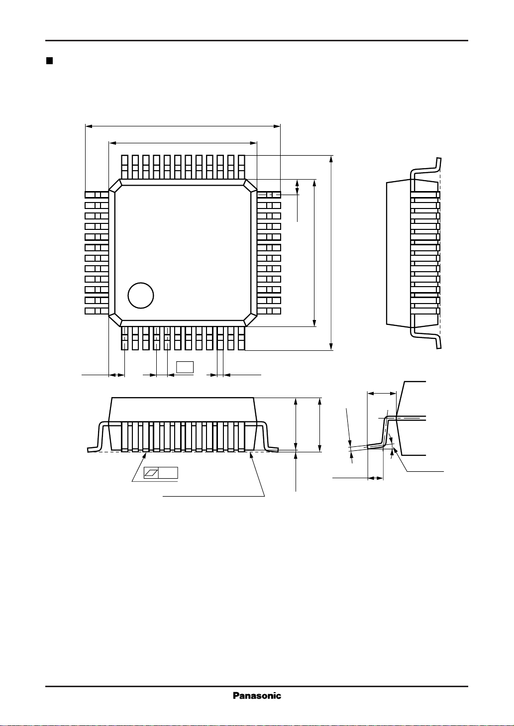
Package Dimensions (Unit:mm)
TQFP048-P-0707
9.0±0.2
±0.2
7.0
36 25
37
48
(0.75)
24
(0.75)
7.0±0.2
9.0±0.2
13
1
0.5
12
0.2±0.1
(1.0)
±0.20.1±0.1
2.5
0.1
0.05
-
+0.10
2.9 max.
0.15
0.5±0.2
0 to 10°
SEATING PLANE
7

 Loading...