

Page 1
Color TFT LCD Driver
MN838850
Source Driver for LCD Panel Drive
■ Overview
The MN838850 converts digital display data from a personal computer or an engineering workstation to analog signal
voltages to allow those signals to be displayed on a color TFT LCD panel.
■ Features
• Includes a built-in D/A converter and accepts 8-bit digital input data for 16.7-million color display.
• Output dynamic range: 14.6 V
• Supports both dot inversion drive and source inversion drive schemes.
• Number of drive outputs: 384
• Input data bus: acquires two pixels at the same time
• Supports control of data inversion at each clock cycle.
• Supports γ correction.
• Adopts a drive scheme that does not require precharging.
• Allows serial cascade connection.
• The clock is automatically stopped after the acquisition of a fixed amount of data.
• The shift register shift direction can be set to be either left-to-right or right-to-left.
• Digital circuit block features low-voltage operation:
2.7 to 3.6 V
• Maximum operating clock frequency:
50 MHz (3.1 to 3.6 V), 40 MHz (2.7 to 3.6 V)
(when AVDD = 15 V)
P-P
■ Applications
•
TFT LCD panels
1
Page 2
MN838850 Color TFT LCD Driver
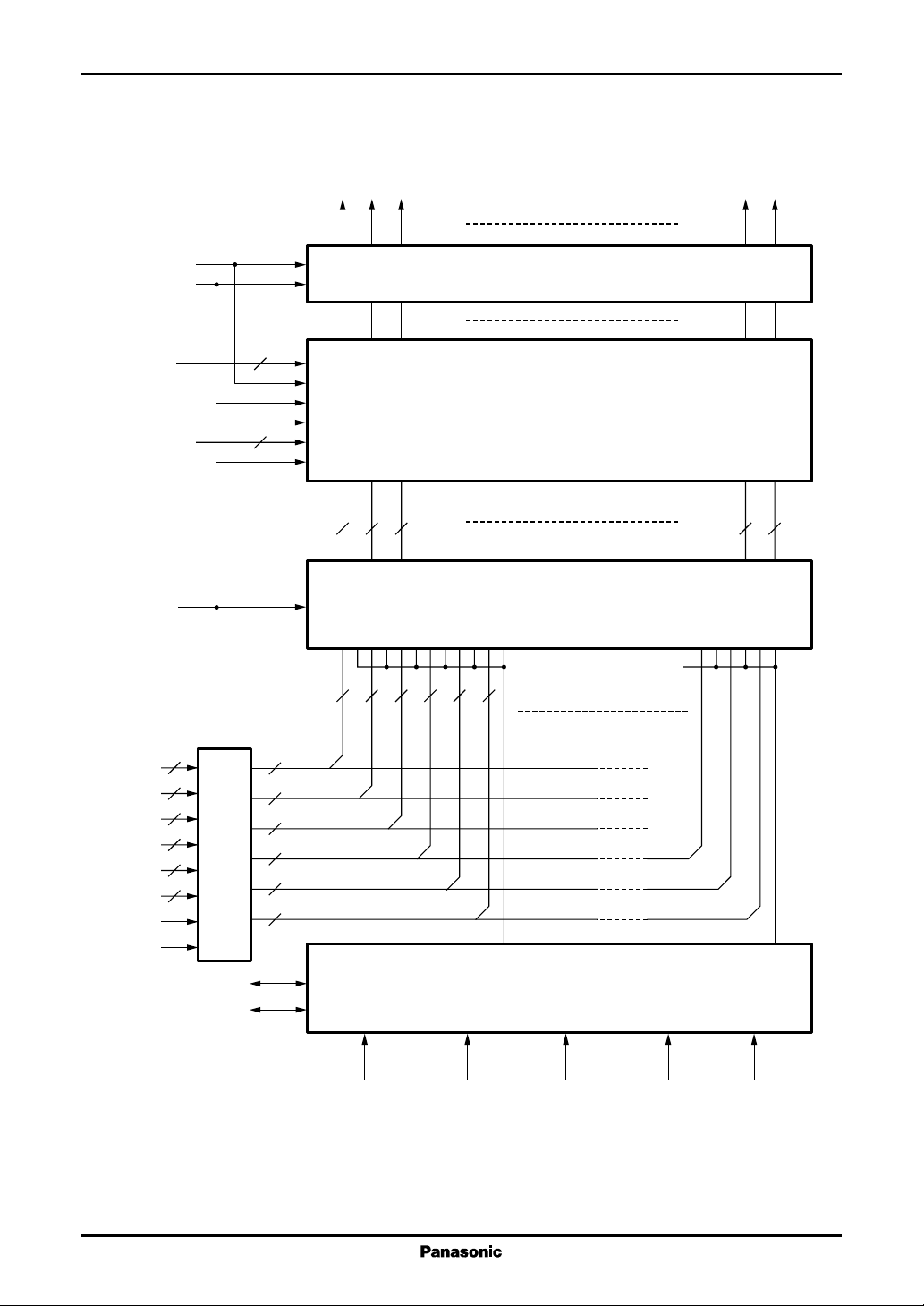
■ Block Diagram
Y1
Y2
Y3
Y383
Y384
VREF0 to 9
VOPU, VOPL
D00 to D07
D10 to D17
D20 to D27
D30 to D37
D40 to D47
D50 to D57
INV1
INV2
AVDD
AVSS
POL
A
8
8
8
8
8
8
Latch
10
2
Output Circuit
D/A Converter
8 8 88
8
Two-line 384 × 8-bit latch
8 8 8 8 8 8
8
8
8
8
8
8
PLSR
PRSL
DVDD
2
Shift Register
DVSS
RL
FY
TEST
Page 3
Color TFT LCD Driver MN838850
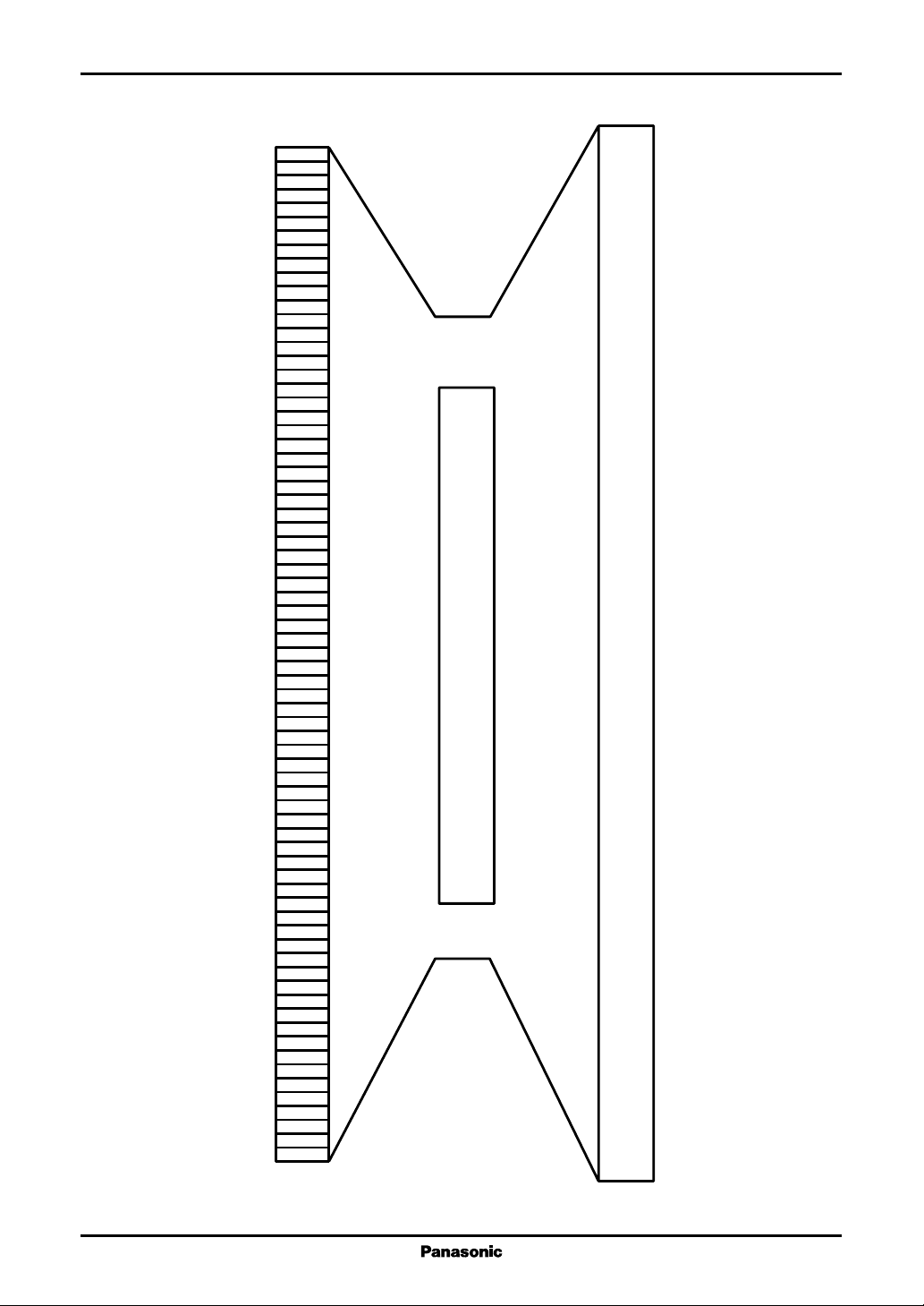
■ Pin Arrangement
Y384
1 PRSL
2D57
3D56
4D55
5D54
6D53
7D52
8D51
9D50
10 D47
11 D46
12 D45
13 D44
14 D43
15 D42
16 D41
17 D40
18 D37
19 D36
20 D35
21 D34
22 D33
23 D32
24 D31
25 D30
26 DVDD
27 TEST
28 RL
29 VOPU
30 VREF9
31 VREF8
32 VREF7
33 VREF6
34 VREF5
35 A VDD
36 A VSS
37 VREF4
38 VREF3
39 VREF2
30 VREF1
41 VREF0
42 VOPL
43 DVSS
44 FY
45 A
46 POL
47 INV2
48 INV1
49 D27
50 D26
51 D25
52 D24
53 D23
54 D22
55 D21
56 D20
57 D17
58 D16
59 D15
60 D14
61 D13
62 D12
63 D11
64 D10
65 D07
66 D06
67 D05
68 D04
69 D03
70 D02
71 D01
72 D00
73 PLSR
Cu Foil Surface Top View
Y383
Y382
Y381
Y380
·
·
·
·
·
·
·
·
·
·
·
·
·
·
·
·
·
·
·
·
·
·
·
·
·
·
·
·
·
·
·
·
·
·
·
·
·
·
·
·
·
·
·
·
·
·
·
·
·
·
·
·
·
·
·
·
·
·
·
·
·
·
·
·
·
·
·
·
·
·
·
·
·
·
·
·
·
·
·
·
·
·
·
·
·
·
·
·
·
·
·
·
·
·
·
·
·
·
·
·
·
·
·
·
·
·
·
·
·
·
·
·
·
·
·
·
·
·
·
·
·
·
·
·
·
·
·
·
·
·
·
·
·
·
·
·
·
·
·
·
·
·
·
·
·
·
·
·
·
·
·
·
·
·
·
·
·
·
·
·
·
·
·
·
·
·
·
·
·
Y5
Y4
Y3
Y2
Y1
3
Page 4
MN838850 Color TFT LCD Driver
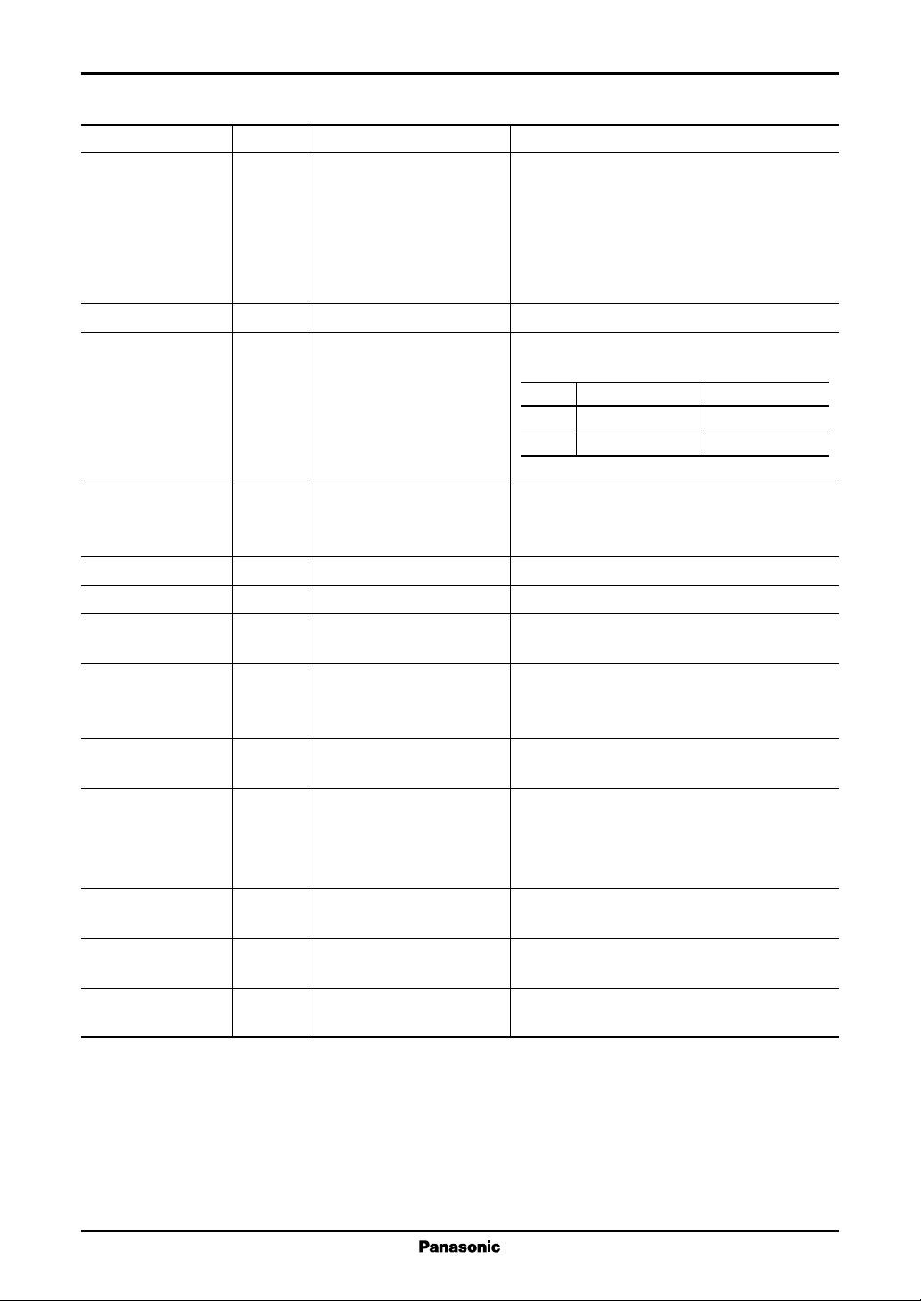
■ Pin Descriptions
Pin No. I/O Pin Name Description
D00 to D07 I Image data input Image data input pins.
D10 to D17 The R, G, and B image signals are input using
D20 to D27 these pins.
D30 to D37 D07, D17, D27, D37, D47, D57 : MSB
D40 to D47 D00, D10, D20, D30, D40, D50 : LSB
D50 to D57
Y1 to Y384 O Image signal output Analog image signal output pins.
PLSR I/O Start pulse input and output Internal shift register start pulse input and
PRSL output pins.
RL = "H" RL = "L"
PLSR Right shift input Left shift output
PRSL Right shift output Left shift input
RL I Shift direction selection Input signal that selects the shift direction.
signal input High: Right shift (Y1 to Y384)
Low: Left shift (Y384 to Y1)
FY I Clock input Data acquisition clock input pin.
A I Analog output control Controls the analog voltage output.
POL I Output polarity reversal Switches the reference voltage for odd and even
control input outputs.
INV1 I Data inversion control input Controls inversion of the input image signal.
INV2 INV1: Used for D2(7 : 0), D1(7 : 0), D0(7 : 0)
INV2: Used for D5(7 : 0), D4(7 : 0), D3(7 : 0)
VREF0 to 9 I γ correction voltage input Inputs the γ correction voltage used by the D/A
converter.
VOPU, VOPL I Analog reference voltage Provides the reference voltage that determines
the analog circuit operating point.
VOPU: Reference voltage for the high side output
VOPL: Reference voltage for the low side output
AVDD I Analog system power supply Provides the power for the analog circuits.
AVSS
DVDD I Digital system power supply Provides the power for the digital circuits.
DVSS
TEST I Test Used for device testing.
(Pull-down resistor: 100 kΩ) This pin must be left open during normal operation.
4
Page 5
Color TFT LCD Driver MN838850
■ Functional Description
•
Relationship between the data input and the analog output pins
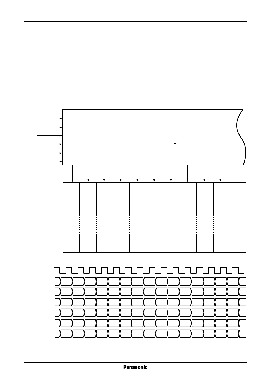
The input mode used by this IC is a two-pixel mode in which the data for two pixels is input in parallel from the D0(7:0),
D1(7:0), D2(7:0), D3(7:0), D4(7:0), and D5(7:0) input ports.
The correspondence between the data input ports and the output pins is as follows.
Y(6n−5) = D00 to D07 Y(6n−2) = D30 to D37
Y(6n−4) = D10 to D17 Y(6n−1) = D40 to D47
Y(6n−3) = D20 to D27 Y(6n) = D50 to D57 (n = 1, 2, ······, 64)
Figure 1 shows an example of color data and pin connections when RL is high.
This example shows the case where the pixels are in the order R, B, G starting at the left edge of the LCD panel.
D00 to D07
R2n-1
D10 to D17
B2n-1
G2n-1
R2n
B2n
G2n
(n=1..)
D20 to D27
D30 to D37
D40 to D47
D50 to D57
Y1
Y2
Y3
Y4
MN838850
Y5
Y6
Y7
Y8
Y9
Y10
············
FY
D0(7 : 0)
D1(7 : 0)
D2(7 : 0)
D3(7 : 0)
D4(7 : 0)
D5(7 : 0)
R1 B1 R2 B2 G2 R3 B3 G3 R4
R1 B1 R2 B2 G2
R1 B1
G1
G1
G1 R2 B2 G2
R3 B3 G3 R4
R3 B3 G3 R4
LCD Panel
R1
R3
R5
R7
R9
R11
R13
R15
R17
R19
R21
R23
R25
B1
B3
B5
B7
B9
B11
B13
B15
B17
B19
B21
B23
B25
G1
G3
G5
G7
G9
G11
G13
G15
G17
G19
G21
G23
G25
R2
R4
R6
R8
R10
R12
R14
R16
R18
R20
R22
R24
R26
B2
B4
B6
B8
B10
B12
B14
B16
B18
B20
B22
B24
B26
G2
G4
G6
G8
G10
G12
G14
G16
G18
G20
G22
G24
G26
···
···
···
R27
B27
G27
R28
B28
G28
Figure 1 Relationship between Input and Output Pins (When RL is high and the shift direction is Y1 to Y384)
5
Page 6
MN838850 Color TFT LCD Driver
■ Functional Description (continued)
•
Relationship between the data input and the analog output pins (continued)
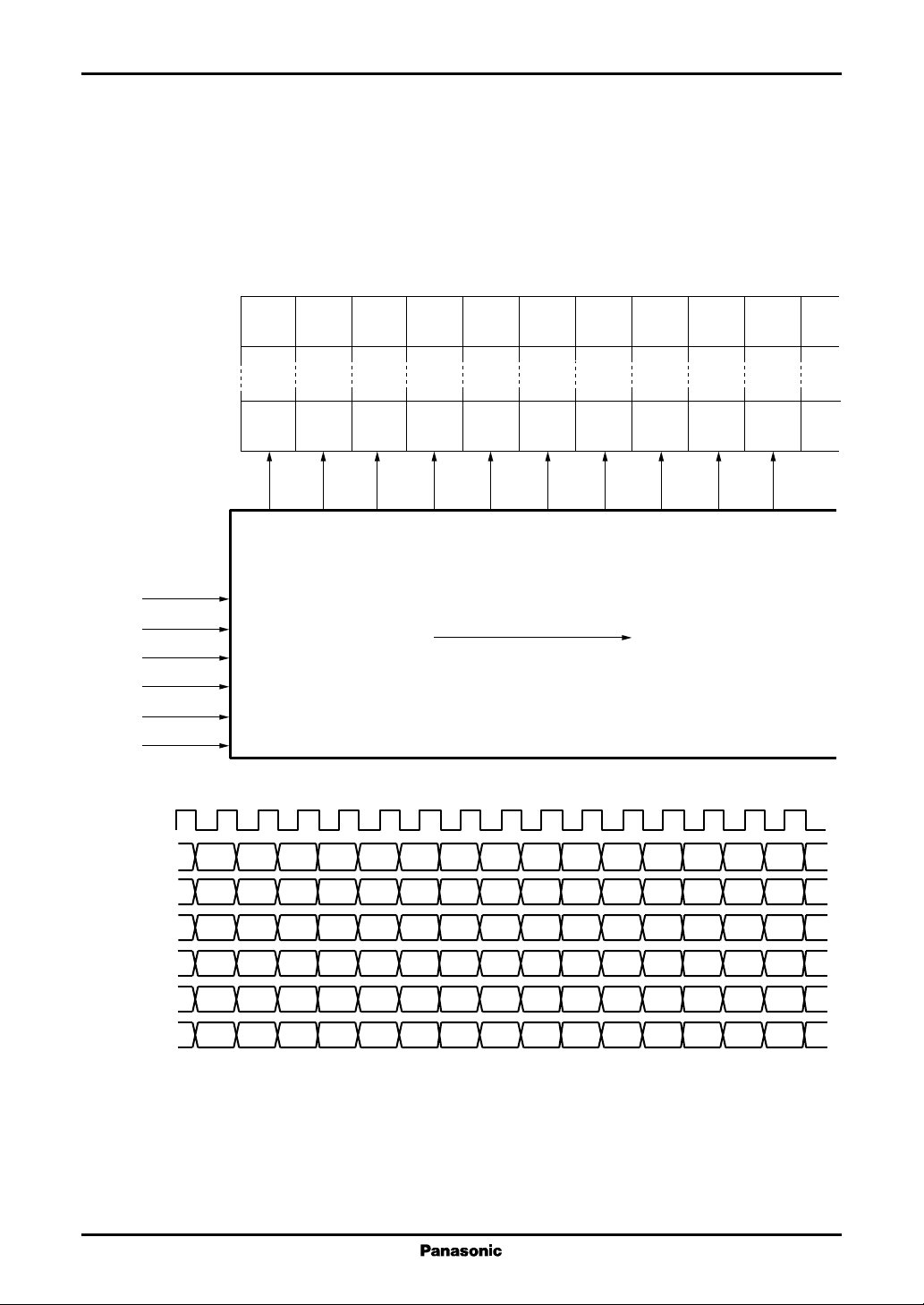
The following presents the case with the same LCD panel color arrangement as figure 1 but with RL low.
In figure 2, R1 corresponds to Y384, B1 to Y383, and G1 to Y382. Note that the relationship between the color data
and the data ports here differs from that in figure 1.
LCD Panel
R2n-1
B2n-1
G2n-1
R2n
B2n
G2n
(n=1..)
FY
D50 to D57
D40 to D47
D30 to D37
D20 to D27
D10 to D17
D00 to D07
R1 B1 R2 B2 G2
R1 B1G1G1 R2 B2 G2
Y384
Y383
Y382
Y381
Y380
MN838850
R3 B3 G3 R4
R3 B3 G3 R4
Y379
Y378
Y377
Y376
Y377
···
···
·········
G2
G4
G6
G8
G10
G12
G14
G16
G18
G20
G22
G24
B24
R24
G23
B23
R23
G26
B26
R26
G25
B25
R25
D0(7 : 0)
B2
B4
B6
B8
B10
B12
B14
B16
B18
B20
R20
G19
B19
R19
B22
R22
G21
B21
R21
D1(7 : 0)
R2
R4
R6
R8
R10
R12
R14
R16
G15
B15
R15
R18
G17
B17
R17
D2(7 : 0)
G1
G3
G5
G7
G9
G11
B11
R11
G13
B13
R13
D3(7 : 0)
B1
B3
B5
B7
R7
B9
R9
D4(7 : 0)
R1
R3
D5(7 : 0)
Figure 2 Relationship between Input and Output Pins (When RL is low and the shift direction is Y384 to Y1)
6
R5
G28
B28
R28
G27
B27
R27
Page 7
Color TFT LCD Driver MN838850
■ Functional Description (continued)
•
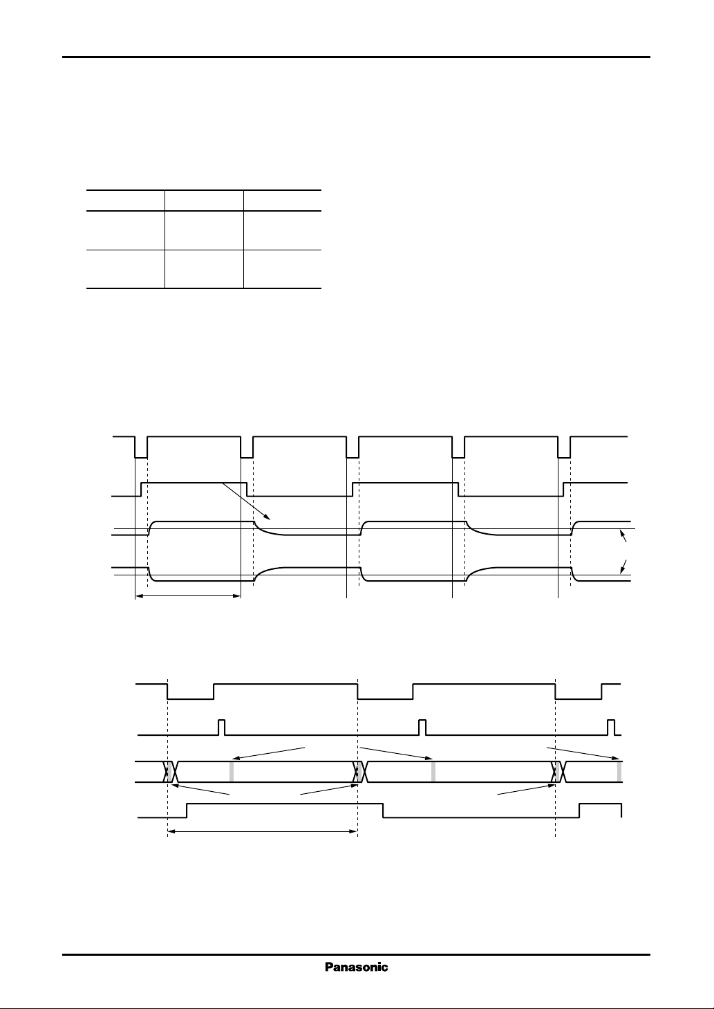
Dot inversion drive
Since dot inversion drive is used, the analog output voltages with respect to the opposite electrode voltage differ in polarity
for each of the odd and even numbered output pins. This output voltage polarity is controlled by POL. The table below
lists the correspondence between the POL polarity setting, the analog output polarity and the VREF used.
POL Y2n-1 Y2n
"L"
"H"
The POL switching timing is presented below.
POL should be switched during the period when A is low, after the last data has been input, and before the next start
signal has been input. The POL signal level is acquired by the device internally on the falling edge of the A signal. The
output polarity is determined by the acquired signal level.
A
Positive polarity Negative polarity
VREF9 to 5 VREF4 to 0
Negative polarity Positive polarity
VREF4 to 0 VREF9 to 5
POL
Y
2n-1
Y
2n
(n=1 to 192)
A
Start Signal
Dxx
POL
One horizontal period
One horizontal period
Negative
polarity
Positive
polarity
Positive
polarity
Negative
polarity
POL Switching Timing
First data First data
Last data
Details of the POL Switching Timing
Last data
Negative
polarity
Positive
polarity
Opposite electrode
voltages
7
Page 8
MN838850 Color TFT LCD Driver
■ Functional Description (continued)
•
Dot inversion drive (continued)
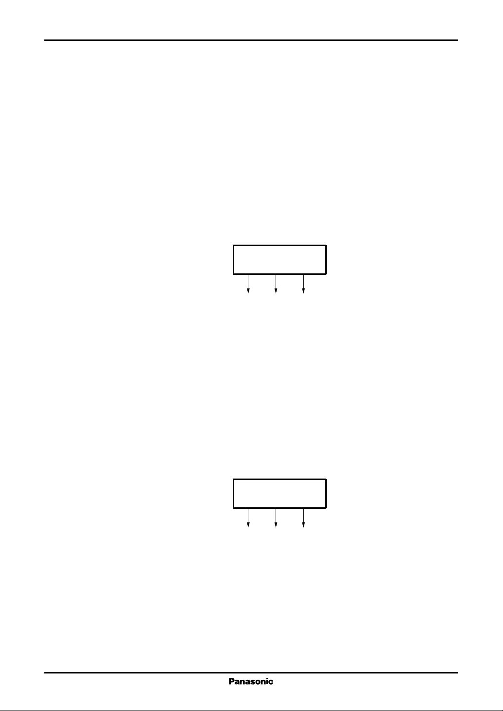
Next we describe dot inversion drive operation.
The symbol "+" here means a voltage that is positive with respect to the voltage on the opposite electrode, and "−" means
a voltage that is negative with respect to the voltage on the opposite electrode.
The figure below shows the dot inversion drive operation.
Since POL is low in the first line of the first field, Y1 will be + and Y2 will be −, that is, odd-numbered output pins
will have positive polarity and even-numbered output pins will have negative polarity.
Since POL is switched to high for the second line, odd-numbered output pins will have negative polarity and evennumbered output pins will have positive polarity.
Thereafter, the polarity of the output voltages is determined by the POL polarity.
In the second field, the POL polarity will be the opposite of what it was for the first field, so the output voltage polarities
will be reversed.
Y1
Y2
Y3
Field 1 Line 1 +−+ "L"
Line 2 −+− "H"
Line 3 +−+ "L"
Line 4 −+− "H"
·
·
·
·
·
·
Field 2 Line 1 −+− "H"
Line 2 +−+ "L"
Line 3 −+− "H"
POL
Note that if POL is inverted not every line, but only every field, the output polarities will be as shown below.
Y1
Y2
Y3
Field 1 Line 1 +−+ "L"
Line 2 +−+ "L"
Line 3 +−+ "L"
·
·
·
·
·
·
Field 2 Line 1 −+− "H"
Line 2 −+− "H"
Line 3 −+− "H"
8
POL
Page 9
Color TFT LCD Driver MN838850
■ Functional Description (continued)
•
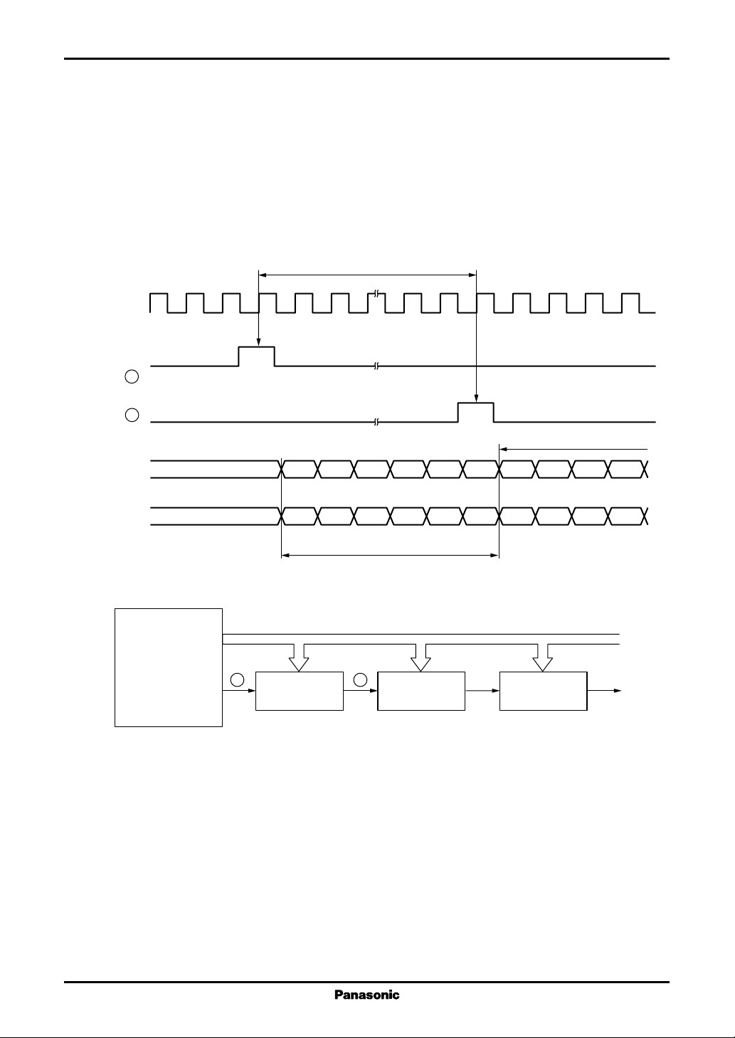
Operation when Connected in Cascade
When RL is high:
Driver A acquires the PLSR start pulse on the rising edge of FY and starts acquiring data on the next FY rising edge.
The PRSL (carry) output will go high 64 clock pulses after the start pulse input and data acquisition will stop one clock
cycle later.
Driver B receives the driver A PRSL rising edge and starts accepting data one clock cycle later.
64 clock cycles
FY
Acquired on the falling
edge of FY.
State of
signal 1
State of
signal 2
Driver B
D00 to D07
D10 to D17
D20 to D27
D30 to D37
D40 to D47
D50 to D57
1 3 5 ··· 125 127 129 131 133
135
4 6 ··· 126 128 130 132 134
2
Data acquired by driver A
246
LCD controller
8-bit RGB data
Start pulse
1 2
PLSR PRSL
Driver A
PLSR PRSL
Driver B
PLSR PRSL
Driver C
9
Page 10
MN838850 Color TFT LCD Driver
■ Functional Description (continued)
•
Relationship between input data values and output voltages
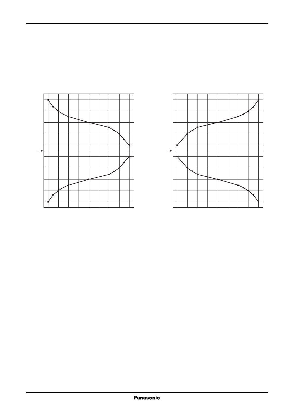
The IC outputs voltages with discrete values and differing polarities for the odd and even output pins with respect to
the common electrode. The output voltage is determined by the input data value, the γ correction voltages (VREF0 to
VREF9), VOPL, VOPU, and POL.
AVDD
Output V oltage
Common
voltage
00 1F 3F 5F 7F 9F BF DF FF
Input data Input data (Hexadecimal)
Relationship between Input Data and Output Voltage
(VREF0 > VREF1 > VREF2 > VREF3 > VREF4,
VREF5 > VREF6 > VREF7 > VREF8 > VREF9)
A VDD
Output V oltage
Common
voltage
00 1F 3F 5F 7F 9F BF DF FF
Input data
Relationship between Input Data and Output Voltage
(VREF0 < VREF1 < VREF2 < VREF3 < VREF4,
VREF5 < VREF6 < VREF7 < VREF8 < VREF9)
10
Page 11
Color TFT LCD Driver MN838850
■ Functional Description (continued)
•
Relationship between input data values and output voltages (continued)
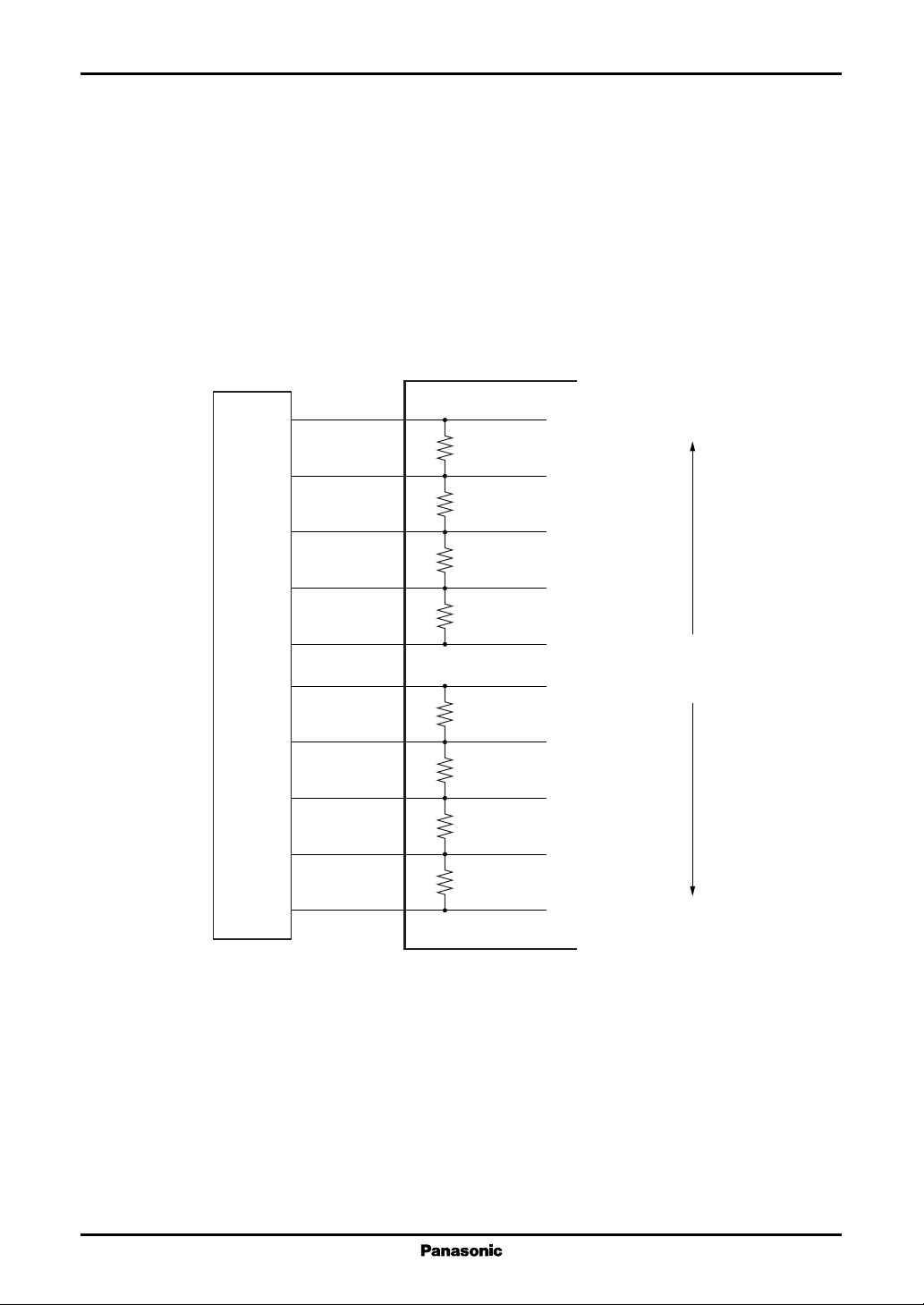
Apply the voltages for the γ correction to the pins VREF0 to VREF9.
The γ correction voltage input pins are divided into two groups: the high-level output control group and the low-level
output control group, and each group is connected in series with resistors. Each of these resistor series has a total
typical value of 14 kΩ.
This structure is shown in the figure. The typical values of the resistors are shown in parentheses.
Note that since these voltages are resistor divided internally, the voltages applied to the VREF pins should be applied
through a low-impedance circuit. If the voltages are directly applied by the resistor divider, the desired output voltages
may not result.
IC internal circuits
VREF9
R0 (2000 Ω)
VREF8
Data correspondence
High-level
output side
FF
VREF7
VREF6
VREF5
VREF4
VREF3
VREF2
External reference voltage generating circuit
VREF1
VREF0
R1 (3800 Ω)
R2 (4500 Ω)
R3 (3700 Ω)
R4 (3700 Ω)
R5 (4500 Ω)
R6 (3800 Ω)
R7 (2000 Ω)
Low-level
output side
00
00
FF
11
Page 12
MN838850 Color TFT LCD Driver
■ Functional Description (continued)
•
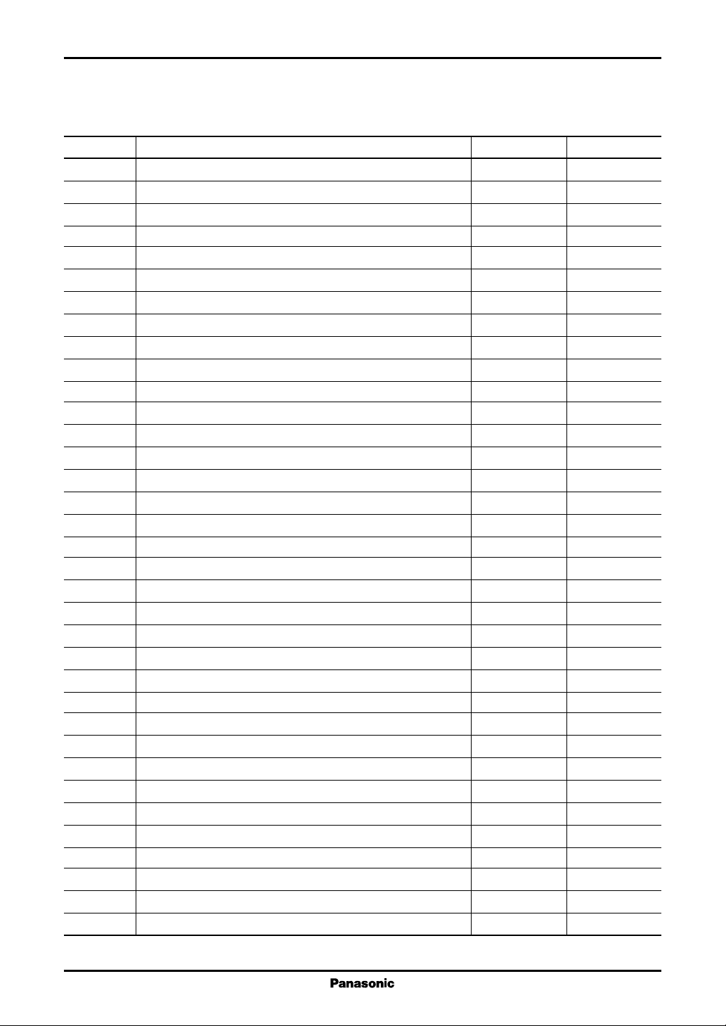
Table 1 Relationship between VREF Voltages and Analog Output Voltages (High-level side) (Values are examples)
VREF5 = 9.200, VREF6 = 10.635, VREF7 = 12.380, VREF8 = 13.854, VREF9 = 14.630, VOPU = 11.250
Display data Logical expression Voltage level
00 VOPU × 63/31− (42 × VREF8+1238 × VREF9) /1240 7.787 0.026
01 VOPU × 63/31− (84 × VREF8+1196 × VREF9) /1240 7.813 0.026
02 VOPU × 63/31− (126 × VREF8+1154 × VREF9) /1240 7.839 0.026
·
·
·
0D VOPU × 63/31− (588 × VREF8+692 × VREF9) /1240 8.128 0.026
0E VOPU × 63/31− (630 × VREF8+650 × VREF9) /1240 8.155 0.026
0F VOPU × 63/31− (672 × VREF8+608 × VREF9) /1240 8.181 0.023
10 VOPU × 63/31− (710 × VREF8+570 × VREF9) /1240 8.205 0.023
11 VOPU × 63/31− (748 × VREF8+532 × VREF9) /1240 8.228 0.023
12 VOPU × 63/31− (786 × VREF8+494 × VREF9) /1240 8.252 0.023
·
·
·
1D VOPU × 63/31− (1204 × VREF8+76 × VREF9) /1240 8.514 0.023
1E VOPU × 63/31− (1242 × VREF8+38 × VREF9) /1240 8.537 0.023
1F VOPU × 63/31− (1280 × VREF8+0 × VREF9) /1240 8.561 0.020
20 VOPU × 63/31− (32 × VREF7+2400 × VREF8) /2356 8.581 0.020
21 VOPU × 63/31− (64 × VREF7+2368 × VREF8) /2356 8.601 0.020
22 VOPU × 63/31− (96 × VREF7+2336 × VREF8) /2356 8.621 0.020
·
·
·
2D VOPU × 63/31− (448 × VREF7+1984 × VREF8) /2356 8.841 0.020
2E VOPU × 63/31− (480 × VREF7+1952 × VREF8) /2356 8.861 0.020
2F VOPU × 63/31− (512 × VREF7+1920 × VREF8) /2356 8.882 0.016
30 VOPU × 63/31− (538 × VREF7+1894 × VREF8) /2356 8.898 0.016
31 VOPU × 63/31− (564 × VREF7+1868 × VREF8) /2356 8.914 0.016
32 VOPU × 63/31− (590 × VREF7+1842 × VREF8) /2356 8.930 0.016
·
·
·
3D VOPU × 63/31− (876 × VREF7+1556 × VREF8) /2356 9.109 0.016
3E VOPU × 63/31− (902 × VREF7+1530 × VREF8) /2356 9.125 0.016
3F VOPU × 63/31− (928 × VREF7+1504 × VREF8) /2356 9.142 0.015
40 VOPU × 63/31− (953 × VREF7+1479 × VREF8) /2356 9.157 0.015
41 VOPU × 63/31− (978 × VREF7+1454 × VREF8) /2356 9.173 0.015
42 VOPU × 63/31− (1003 × VREF7+1429 × VREF8) /2356 9.189 0.015
·
·
·
4D VOPU × 63/31− (1278 × VREF7+1154 × VREF8) /2356 9.361 0.015
4E VOPU × 63/31− (1303 × VREF7+1129 × VREF8) /2356 9.376 0.015
4F VOPU × 63/31− (1328 × VREF7+1104 × VREF8) /2356 9.392 0.015
Voltage level difference
12
Page 13
Color TFT LCD Driver MN838850
■ Functional Description (continued)
•
Table 1 (continued) Relationship between VREF Voltages and Analog Output Voltages (High-level side) (Values are examples)
VREF5 = 9.200, VREF6 = 10.635, VREF7 = 12.380, VREF8 = 13.854, VREF9 = 14.630, VOPU = 11.250
Display data Logical expression Voltage level
50 VOPU × 63/31− (1353 × VREF7+1079 × VREF8) /2356 9.408 0.015
51 VOPU × 63/31− (1378 × VREF7+1054 × VREF8) /2356 9.423 0.015
52 VOPU × 63/31− (1403 × VREF7+1029 × VREF8) /2356 9.439 0.015
·
·
·
5D VOPU × 63/31− (1678 × VREF7+754 × VREF8) /2356 9.611 0.015
5E VOPU × 63/31− (1703 × VREF7+729 × VREF8) /2356 9.627 0.015
5F VOPU × 63/31− (1728 × VREF7+704 × VREF8) /2356 9.642 0.013
60 VOPU × 63/31− (1750 × VREF7+682 × VREF8) /2356 9.656 0.013
61 VOPU × 63/31− (1772 × VREF7+660 × VREF8) /2356 9.670 0.013
62 VOPU × 63/31− (1794 × VREF7+638 × VREF8) /2356 9.683 0.013
·
·
·
6D VOPU × 63/31− (2036 × VREF7+396 × VREF8) /2356 9.835 0.013
6E VOPU × 63/31− (2058 × VREF7+374 × VREF8) /2356 9.849 0.013
6F VOPU × 63/31− (2080 × VREF7+352 × VREF8) /2356 9.862 0.013
70 VOPU × 63/31− (2102 × VREF7+330 × VREF8) /2356 9.876 0.013
71 VOPU × 63/31− (2124 × VREF7+308 × VREF8) /2356 9.890 0.013
72 VOPU × 63/31− (2146 × VREF7+286 × VREF8) /2356 9.904 0.013
·
·
·
7D VOPU × 63/31− (2388 × VREF7+44 × VREF8) /2356 10.055 0.013
7E VOPU × 63/31− (2410 × VREF7+22 × VREF8) /2356 10.069 0.013
7F VOPU × 63/31− (2432 × VREF7+0 × VREF8) /2356 10.083 0.013
80 VOPU × 63/31− (11 × VREF6+1429 × VREF7) /1395 10.096 0.013
81 VOPU × 63/31− (22 × VREF6+1418 × VREF7) /1395 10.110 0.013
82 VOPU × 63/31− (33 × VREF6+1407 × VREF7) /1395 10.124 0.013
·
·
·
8D VOPU × 63/31− (154 × VREF6+1286 × VREF7) /1395 10.275 0.013
8E VOPU × 63/31− (165 × VREF6+1275 × VREF7) /1395 10.289 0.013
8F VOPU × 63/31− (176 × VREF6+1264 × VREF7) /1395 10.303 0.013
90 VOPU × 63/31− (187 × VREF6+1253 × VREF7) /1395 10.317 0.013
91 VOPU × 63/31− (198 × VREF6+1242 × VREF7) /1395 10.330 0.013
92 VOPU × 63/31− (209 × VREF6+1231 × VREF7) /1395 10.344 0.013
·
·
·
9D VOPU × 63/31− (330 × VREF6+1110 × VREF7) /1395 10.495 0.013
9E VOPU × 63/31− (341 × VREF6+1099 × VREF7) /1395 10.509 0.013
9F VOPU × 63/31− (352 × VREF6+1088 × VREF7) /1395 10.523 0.016
Voltage level difference
13
Page 14
MN838850 Color TFT LCD Driver
■ Functional Description (continued)
•
Table 1 (continued) Relationship between VREF Voltages and Analog Output Voltages (High-level side) (Values are examples)
VREF5 = 9.200, VREF6 = 10.635, VREF7 = 12.380, VREF8 = 13.854, VREF9 = 14.630, VOPU = 11.250
Display data Logical expression Voltage level
A0 VOPU × 63/31− (365 × VREF6+1075 × VREF7) /1395 10.539 0.016
A1 VOPU × 63/31− (378 × VREF6+1062 × VREF7) /1395 10.556 0.016
A2 VOPU × 63/31− (391 × VREF6+1049 × VREF7) /1395 10.572 0.016
·
·
·
AD VOPU × 63/31− (534 × VREF6+906 × VREF7) /1395 10.751 0.016
AE VOPU × 63/31− (547 × VREF6+893 × VREF7) /1395 10.767 0.016
AF VOPU × 63/31− (560 × VREF6+880 × VREF7) /1395 10.783 0.016
B0 VOPU × 63/31− (573 × VREF6+867 × VREF7) /1395 10.800 0.016
B1 VOPU × 63/31− (586 × VREF6+854 × VREF7) /1395 10.816 0.016
B2 VOPU × 63/31− (599 × VREF6+841 × VREF7) /1395 10.832 0.016
·
·
·
BD VOPU × 63/31− (742 × VREF6+698 × VREF7) /1395 11.011 0.016
BE VOPU × 63/31− (755 × VREF6+685 × VREF7) /1395 11.027 0.016
BF VOPU × 63/31− (768 × VREF6+672 × VREF7) /1395 11.043 0.022
C0 VOPU × 63/31− (786 × VREF6+654 × VREF7) /1395 11.066 0.022
C1 VOPU × 63/31− (804 × VREF6+636 × VREF7) /1395 11.089 0.022
C2 VOPU × 63/31− (822 × VREF6+618 × VREF7) /1395 11.111 0.022
·
·
·
CD VOPU × 63/31− (1020 × VREF6+420 × VREF7) /1395 11.359 0.022
CE VOPU × 63/31− (1038 × VREF6+402 × VREF7) /1395 11.381 0.022
CF VOPU × 63/31− (1056 × VREF6+384 × VREF7) /1395 11.404 0.030
D0 VOPU × 63/31− (1080 × VREF6+360 × VREF7) /1395 11.434 0.030
D1 VOPU × 63/31− (1104 × VREF6+336 × VREF7) /1395 11.464 0.030
D2 VOPU × 63/31− (1128 × VREF6+312 × VREF7) /1395 11.494 0.030
·
·
·
DD VOPU × 63/31− (1392 × VREF6+48 × VREF7) /1395 11.824 0.030
DE VOPU × 63/31− (1416 × VREF6+24 × VREF7) /1395 11.854 0.030
DF VOPU × 63/31− (1440 × VREF6+0 × VREF7) /1395 11.884 0.041
E0 VOPU × 63/31− (66 × VREF5+2302 × VREF6) /2294 11.926 0.041
E1 VOPU × 63/31− (132 × VREF5+2236 × VREF6) /2294 11.967 0.041
E2 VOPU × 63/31− (198 × VREF5+2170 × VREF6) /2294 12.008 0.041
·
·
·
ED VOPU × 63/31− (924 × VREF5+1444 × VREF6) /2294 12.462 0.041
EE VOPU × 63/31− (990 × VREF5+1378 × VREF6) /2294 12.504 0.041
EF VOPU × 63/31− (1056 × VREF5+1312 × VREF6) /2294 12.545 0.051
Voltage level difference
14
Page 15
Color TFT LCD Driver MN838850
■ Functional Description (continued)
•
Table 1 (continued) Relationship between VREF Voltages and Analog Output Voltages (High-level side) (Values are examples)
VREF5 = 9.200, VREF6 = 10.635, VREF7 = 12.380, VREF8 = 13.854, VREF9 = 14.630, VOPU = 11.250
Display data Logical expression Voltage level
F0 VOPU × 63/31− (1138 × VREF5+1230 × VREF6) /2294 12.596 0.051
F1 VOPU × 63/31− (1220 × VREF5+1148 × VREF6) /2294 12.647 0.051
F2 VOPU × 63/31− (1302 × VREF5+1066 × VREF6) /2294 12.699 0.051
·
·
·
FD VOPU × 63/31− (2204 × VREF5+164 × VREF6) /2294 13.263 0.051
FE VOPU × 63/31− (2286 × VREF5+82 × VREF6) /2294 13.314 0.051
FF VOPU × 63/31− (2368 × VREF5+0 × VREF6) /2294 13.366
•
Table 2 Relationship between VREF Voltages and Analog Output Voltages (Low-level side) (Values are examples)
VREF0 = 1.760, VREF1 = 2.536, VREF2 = 4.010, VREF3 = 5.755, VREF4 = 7.190, VOPL = 3.750
Display data Logical expression Voltage level
00 VOPL × 63/31− (42 × VREF1+1238 × VREF0) /1240 5.777 0.026
01 VOPL × 63/31− (84 × VREF1+1196 × VREF0) /1240 5.751 0.026
02 VOPL × 63/31− (126 × VREF1+1154 × VREF0) /1240 5.725 0.026
·
·
·
0D VOPL × 63/31− (588 × VREF1+692 × VREF0) /1240 5.436 0.026
0E VOPL × 63/31− (630 × VREF1+650 × VREF0) /1240 5.410 0.026
0F VOPL × 63/31− (672 × VREF1+608 × VREF0) /1240 5.383 0.023
10 VOPL × 63/31− (710 × VREF1+570 × VREF0) /1240 5.360 0.023
11 VOPL × 63/31− (748 × VREF1+532 × VREF0) /1240 5.336 0.023
12 VOPL × 63/31− (786 × VREF1+494 × VREF0) /1240 5.312 0.023
·
·
·
1D VOPL × 63/31− (1204 × VREF1+76 × VREF0) /1240 5.051 0.023
1E VOPL × 63/31− (1242 × VREF1+38 × VREF0) /1240 5.027 0.023
1F VOPL × 63/31− (1280 × VREF1+0 × VREF0) /1240 5.003 0.020
20 VOPL × 63/31− (32 × VREF2+2400 × VREF1) /2356 4.983 0.020
21 VOPL × 63/31− (64 × VREF2+2368 × VREF1) /2356 4.963 0.020
22 VOPL × 63/31− (96 × VREF2+2336 × VREF1) /2356 4.943 0.020
·
·
·
2D VOPL × 63/31− (448 × VREF2+1984 × VREF1) /2356 4.723 0.020
2E VOPL × 63/31− (480 × VREF2+1952 × VREF1) /2356 4.703 0.020
2F VOPL × 63/31− (512 × VREF2+1920 × VREF1) /2356 4.683 0.016
Voltage level difference
Voltage level difference
15
Page 16
MN838850 Color TFT LCD Driver
■ Functional Description (continued)
•
Table 2 (continued) Relationship between VREF Voltages and Analog Output Voltages (Low-level side) (Values are examples)
VREF0 = 1.760, VREF1 = 2.536, VREF2 = 4.010, VREF3 = 5.755, VREF4 = 7.190, VOPL = 3.750
Display data Logical expression Voltage level
30 VOPL × 63/31− (538 × VREF2+1894 × VREF1) /2356 4.666 0.016
31 VOPL × 63/31− (564 × VREF2+1868 × VREF1) /2356 4.650 0.016
32 VOPL × 63/31− (590 × VREF2+1842 × VREF1) /2356 4.634 0.016
·
·
·
3D VOPL × 63/31− (876 × VREF2+1556 × VREF1) /2356 4.455 0.016
3E VOPL × 63/31− (902 × VREF2+1530 × VREF1) /2356 4.439 0.016
3F VOPL × 63/31− (928 × VREF2+1504 × VREF1) /2356 4.422 0.015
40 VOPL × 63/31− (953 × VREF2+1479 × VREF1) /2356 4.407 0.015
41 VOPL × 63/31− (978 × VREF2+1454 × VREF1) /2356 4.391 0.015
42 VOPL × 63/31− (1003 × VREF2+1429 × VREF1) /2356 4.376 0.015
·
·
·
4D VOPL × 63/31− (1278 × VREF2+1154 × VREF1) /2356 4.203 0.015
4E VOPL × 63/31− (1303 × VREF2+1129 × VREF1) /2356 4.188 0.015
4F VOPL × 63/31− (1328 × VREF2+1104 × VREF1) /2356 4.172 0.015
50 VOPL × 63/31− (1353 × VREF2+1079 × VREF1) /2356 4.157 0.015
51 VOPL × 63/31− (1378 × VREF2+1054 × VREF1) /2356 4.141 0.015
52 VOPL × 63/31− (1403 × VREF2+1029 × VREF1) /2356 4.125 0.015
·
·
·
5D VOPL × 63/31− (1678 × VREF2+754 × VREF1) /2356 3.953 0.015
5E VOPL × 63/31− (1703 × VREF2+729 × VREF1) /2356 3.938 0.015
5F VOPL × 63/31− (1728 × VREF2+704 × VREF1) /2356 3.922 0.013
60 VOPL × 63/31− (1750 × VREF2+682 × VREF1) /2356 3.908 0.013
61 VOPL × 63/31− (1772 × VREF2+660 × VREF1) /2356 3.894 0.013
62 VOPL × 63/31− (1794 × VREF2+638 × VREF1) /2356 3.881 0.013
·
·
·
6D VOPL × 63/31− (2036 × VREF2+396 × VREF1) /2356 3.729 0.013
6E VOPL × 63/31− (2058 × VREF2+374 × VREF1) /2356 3.716 0.013
6F VOPL × 63/31− (2080 × VREF2+352 × VREF1) /2356 3.702 0.013
70 VOPL × 63/31− (2102 × VREF2+330 × VREF1) /2356 3.688 0.013
71 VOPL × 63/31− (2124 × VREF2+308 × VREF1) /2356 3.674 0.013
72 VOPL × 63/31− (2146 × VREF2+286 × VREF1) /2356 3.660 0.013
·
·
·
7D VOPL × 63/31− (2388 × VREF2+44 × VREF1) /2356 3.509 0.013
7E VOPL × 63/31− (2410 × VREF2+22 × VREF1) /2356 3.495 0.013
7F VOPL × 63/31− (2432 × VREF2+0 × VREF1) /2356 3.482 0.013
Voltage level difference
16
Page 17
Color TFT LCD Driver MN838850
■ Functional Description (continued)
•
Table 2 (continued) Relationship between VREF Voltages and Analog Output Voltages (Low-level side) (Values are examples)
VREF0 = 1.760, VREF1 = 2.536, VREF2 = 4.010, VREF3 = 5.755, VREF4 = 7.190, VOPL = 3.750
Display data Logical expression Voltage level
80 VOPL × 63/31− (11 × VREF3+1429 × VREF2) /1395 3.468 0.013
81 VOPL × 63/31− (22 × VREF3+1418 × VREF2) /1395 3.454 0.013
82 VOPL × 63/31− (33 × VREF3+1407 × VREF2) /1395 3.440 0.013
·
·
·
8D VOPL × 63/31− (154 × VREF3+1286 × VREF2) /1395 3.289 0.013
8E VOPL × 63/31− (165 × VREF3+1275 × VREF2) /1395 3.275 0.013
8F VOPL × 63/31− (176 × VREF3+1264 × VREF2) /1395 3.261 0.013
90 VOPL × 63/31− (187 × VREF3+1253 × VREF2) /1395 3.248 0.013
91 VOPL × 63/31− (198 × VREF3+1242 × VREF2) /1395 3.234 0.013
92 VOPL × 63/31− (209 × VREF3+1231 × VREF2) /1395 3.220 0.013
·
·
·
9D VOPL × 63/31− (330 × VREF3+1110 × VREF2) /1395 3.069 0.013
9E VOPL × 63/31− (341 × VREF3+1099 × VREF2) /1395 3.055 0.013
9F VOPL × 63/31− (352 × VREF3+1088 × VREF2) /1395 3.041 0.016
A0 VOPL × 63/31− (365 × VREF3+1075 × VREF2) /1395 3.025 0.016
A1 VOPL × 63/31− (378 × VREF3+1062 × VREF2) /1395 3.009 0.016
A2 VOPL × 63/31− (391 × VREF3+1049 × VREF2) /1395 2.992 0.016
·
·
·
AD VOPL × 63/31− (534 × VREF3+906 × VREF2) /1395 2.813 0.016
AE VOPL × 63/31− (547 × VREF3+893 × VREF2) /1395 2.797 0.016
AF VOPL × 63/31− (560 × VREF3+880 × VREF2) /1395 2.781 0.016
B0 VOPL × 63/31− (573 × VREF3+867 × VREF2) /1395 2.765 0.016
B1 VOPL × 63/31− (586 × VREF3+854 × VREF2) /1395 2.748 0.016
B2 VOPL × 63/31− (599 × VREF3+841 × VREF2) /1395 2.732 0.016
·
·
·
BD VOPL × 63/31− (742 × VREF3+698 × VREF2) /1395 2.553 0.016
BE VOPL × 63/31− (755 × VREF3+685 × VREF2) /1395 2.537 0.016
BF VOPL × 63/31− (768 × VREF3+672 × VREF2) /1395 2.521 0.022
C0 VOPL × 63/31− (786 × VREF3+654 × VREF2) /1395 2.498 0.022
C1 VOPL × 63/31− (804 × VREF3+636 × VREF2) /1395 2.476 0.022
C2 VOPL × 63/31− (822 × VREF3+618 × VREF2) /1395 2.453 0.022
·
·
·
CD VOPL × 63/31− (1020 × VREF3+420 × VREF2) /1395 2.205 0.022
CE VOPL × 63/31− (1038 × VREF3+402 × VREF2) /1395 2.183 0.022
CF VOPL × 63/31− (1056 × VREF3+384 × VREF2) /1395 2.160 0.030
Voltage level difference
17
Page 18
MN838850 Color TFT LCD Driver
■ Functional Description (continued)
•
Table 2 (continued) Relationship between VREF Voltages and Analog Output Voltages (Low-level side) (Values are examples)
VREF0 = 1.760, VREF1 = 2.536, VREF2 = 4.010, VREF3 = 5.755, VREF4 = 7.190, VOPL = 3.750
Display data Logical expression Voltage level
D0 VOPL × 63/31− (1080 × VREF3+360 × VREF2) /1395 2.130 0.030
D1 VOPL × 63/31− (1104 × VREF3+336 × VREF2) /1395 2.100 0.030
D2 VOPL × 63/31− (1128 × VREF3+312 × VREF2) /1395 2.070 0.030
·
·
·
DD VOPL × 63/31− (1392 × VREF3+48 × VREF2) /1395 1.740 0.030
DE VOPL × 63/31− (1416 × VREF3+24 × VREF2) /1395 1.710 0.030
DF VOPL × 63/31− (1440 × VREF3+0 × VREF2) /1395 1.680 0.041
E0 VOPL × 63/31− (66 × VREF4+2302 × VREF3) /2294 1.639 0.041
E1 VOPL × 63/31− (132 × VREF4+2236 × VREF3) /2294 1.597 0.041
E2 VOPL × 63/31− (198 × VREF4+2170 × VREF3) /2294 1.556 0.041
·
·
·
ED VOPL × 63/31− (924 × VREF4+1444 × VREF3) /2294 1.102 0.041
EE VOPL × 63/31− (990 × VREF4+1378 × VREF3) /2294 1.061 0.041
EF VOPL × 63/31− (1056 × VREF4+1312 × VREF3) /2294 1.019 0.051
F0 VOPL × 63/31− (1138 × VREF4+1230 × VREF3) /2294 0.968 0.051
F1 VOPL × 63/31− (1220 × VREF4+1148 × VREF3) /2294 0.917 0.051
F2 VOPL × 63/31− (1302 × VREF4+1066 × VREF3) /2294 0.865 0.051
·
·
·
FD VOPL × 63/31− (2204 × VREF4+164 × VREF3) /2294 0.301 0.051
FE VOPL × 63/31− (2286 × VREF4+82 × VREF3) /2294 0.250 0.051
FF VOPL × 63/31− (2368 × VREF4+0 × VREF3) /2294 0.199
Voltage level difference
18
Page 19
Color TFT LCD Driver MN838850
■ Functional Description (continued)
•
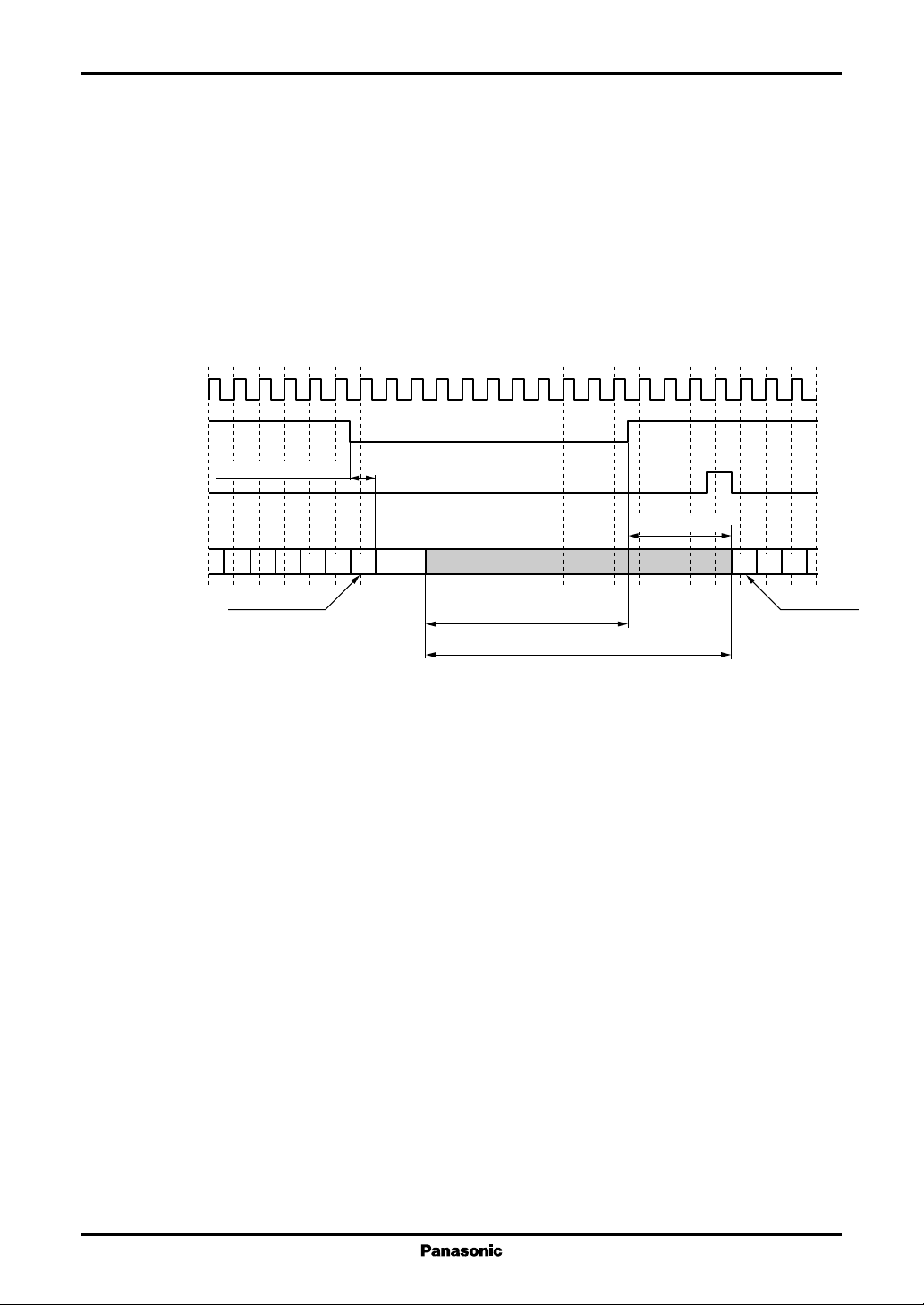
Relationship between the A signal, the image input timing, and the start pulse
The figure below shows the relationship between the A signal, the image data input timing, and the start pulse.
The last data of the image should be input within one clock cycle of the fall of the A signal. Data input two or more clock
cycles later will not be transmitted to the analog outputs and the IC will not be able to output the correct analog voltage.
And also hold the levels of the data bus fixed from 1 µs before the rise of the A signal until 4 clock cycles after the rise
of the A signal. The output analog voltages may be displaced or shifted if the data bus levels are changed with that
timing.
FY
A signal
Start pulse
PLSR(RL = "H")
PRSL(RL = "L")
Data
1 clock cycle (max.)
Last data value
4 clock cycle (min.)
N 1 2 3N-1N-2
First data value
1 µs(min.)
Period during which the data must be held fixed
19
Page 20
MN838850 Color TFT LCD Driver
■ Functional Description (continued)
•
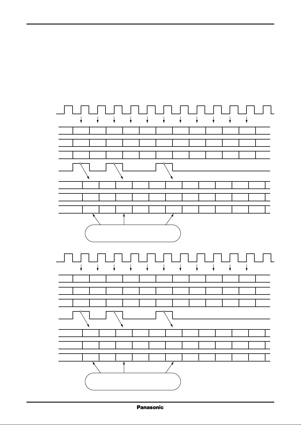
Data inversion control function
All the bits in the input image data can be inverted at the same time, thus creating new data values to be used by controlling
the INV1 and INV2 pins.
INV1 inverts the D0(7:0), D1(7:0), and D2(7:0) data and INV2 inverts the D3(7:0), D4(7:0), and D5(7:0) data.
The figure below shows the inversion control provided by INV1 and INV2 for the input image data.
The input image data and the INV1 and INV2 states are acquired on the same clock cycle, and the data is controlled by
the INV1 and INV2 logic states at that time.
FY
D07 to 00
D17 to 10
D27 to 20
INV1
Internal data
ID07 to 00
ID17 to 10
ID27 to 20
FY
D37 to 30
D47 to 40
00
00 00 0F FF FF FF 00 00 05 08
00 00 05 0F FF FE FF 00 00 05 08
00 00 08 0F FF FD FF 00 00 05 08
FF 00 FF 0F FF 00 FF 00 00 05 08
FF 00 FA 0F FF 01 FF 00 00 05 08
FF 00 F7 0F FF 02 FF 00 00 05 08
Since INV1 is high, All the bits in the
data D0x, D1x, and D2x are inverted.
00 00 0A 0F FF F7 FF 00 00 05 08
00 00 0C 0F FF F4 FF 00 00 05 08
D57 to 50
INV2
Internal data
ID37 to 30
ID47 to 40
ID57 to 50
20
00 00 0F 0F FF F1 FF 00 00 05 08
FF 00 F5 0F FF 08 FF 00 00 05 08
FF 00 F3 0F FF 0B FF 00 00 05 08
FF 00 F0 0F FF 0E FF 00 00 05 08
Since INV1 is high, All the bits in the
data D0x, D1x, and D2x are inverted.
Page 21
Color TFT LCD Driver MN838850
■ Functional Description (continued)
•
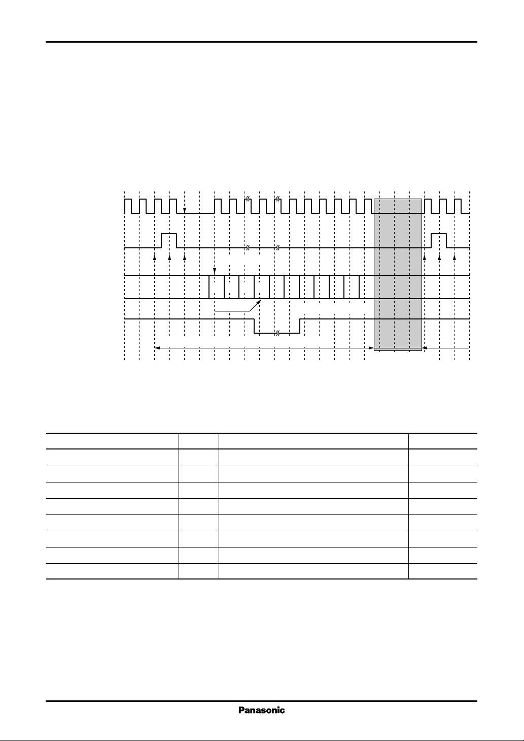
Possible periods of the clock stop
The possible periods of the clock stop in which clock has been stopped are shown below.
The clock signal must be provided during the period starting one clock cycle before the start pulse input and ending 5
clock cycles after the rise of the A signal.
However, if it is not the case that the first data is input with the next clock timing (T) after the input of the start pulse,
the clock may be stopped during the period between the start pulse input and the start of data input. The clock signal
may be stopped at either the high or low level.
FY
T
Start pulse
PLSR(RL = "H")
PRSL(RL = "L")
D
XX
First data
1
3 ··· N
Last data
1 2 3 4 5
A signal
Period during which clock input is required
Period during
which clock input
may be stopped
■ Electrical Characteristics
1. Absolute Maximum Ratings at A
Parameter Symbol Rating Unit
Digital system supply voltage D
Analog system supply voltage A
Digital input voltage V
Analog input voltage V
Digital output voltage V
Analog output voltage V
Operating temperature T
Storage temperature T
Note) The absolute maximum ratings are limiting values under which the device will not be destroyed. Operation is not
guaranteed within these ranges.
= 0 V, D
VSS
VDD
VDD
I1
I2
O1
O2
opr
stg
VSS
= 0 V
− 0.3 to +7.0 V
− 0.3 to +17 V
− 0.3 to D
− 0.3 to A
− 0.3 to D
− 0.3 to A
+0.3 V
VDD
+0.3 V
VDD
+0.3 V
VDD
+0.3 V
VDD
−20 to +75 °C
−40 to +110 °C
21
Page 22
MN838850 Color TFT LCD Driver
■ Electrical Characteristics (continued)
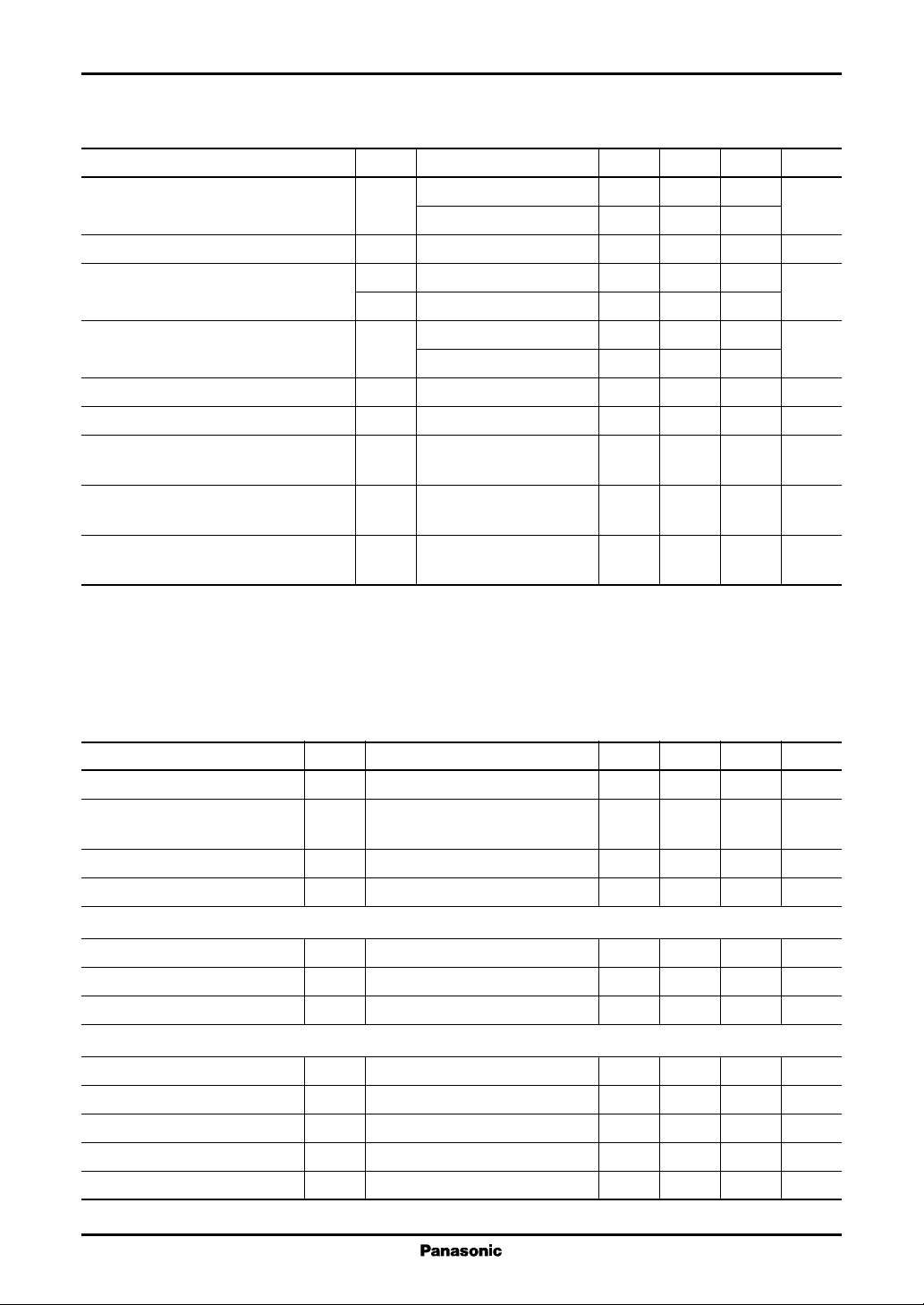
2. Operating Conditions at A
Parameter Symbol Conditions Min Typ Max Unit
Operating digital system supply voltage D
Operating analog system supply voltage A
γ correction voltage input voltage range
Operating frequency D
Digital signal input capacitance C
γ correction voltage input capacitance C
VOPL input voltage range A
VOPU input voltage range A
VREF resistance R
VREF9 to 5, VREF4 to 0
Note) 1. All the A
2. All the A
3. When first applying power, first apply the D
the A
voltages in the reverse order.
power supply pins must be connected to each other directly.
VDD
and D
VSS
voltage. After that apply the VOP and VREF reference voltages. When cutting the power, remove these
VDD
= D
VSS
power supply pins must be connected to each other directly.
VSS
= 0 V, Ta = −20 °C to +75 °C
VSS
VDDfFY max
VDD
V
0 to 4
REF
V
5 to 9
REF
IN
VREF
VREF
VDD
= 50 MHz 3.1 3.6 V
f
= 40 MHz 2.7 3.6
FY max
= 3.1 V to 3.6 V 50 MHz
VDD
D
= 2.7 V to 3.6 V 40
VDD
At 1 MHz 5 pF
At 1 MHz 500 pF
voltage, then apply the logic input pin signal levels, and then apply
14.5 15.5 V
0.2 A
A
/2
VDD
/4 A
VDD
A
VDD
VDD
VDD
/2 V
− 0.2
/4 V
− 0.2 + 0.2
×A
VDD
VDD
× V
3/4− 0.2 3/4+ 0.2
14 kΩ
3. DC Characteristics at D
= 2.7 V to 3.6 V, A
VDD
= 14.5 V to 15.5 V, A
VDD
VSS
= D
= 0 V, Ta = −20 °C to +75 °C
VSS
Parameter Symbol Conditions Min Typ Max Unit
1,3
Operating analog supply current 1
Operating analog supply current 2 I
Operating digital supply current
Digital quiescent supply current I
*
I
SS1
A
SS2
1,2
*
I
SS3
SS4
= 15 V 11 mA
VDD
1, 3
*
With no load
In the clock stopped state 100 µA
39 45 mA
28mA
1) Input pins RL, A, D00 to D07, D10 to D17, D20 to D27, D30 to D37, D40 to D47, D50 to D57, FY, POL, INV1, INV2
High-level input voltage V
Low-level input voltage V
Input leakage current I
IH1
IL1
LI1
0.7 × D
0
VDD
D
0.3× D
VDD
VDD
−10 10 µA
V
V
2) I/O pins PRSL, PLSR
High-level input voltage V
Low-level input voltage V
High-level output voltage V
Low-level output voltage V
Input leakage current I
LI2
IH2
IL2
OH
OL
D
= 3.3 V, IO = −5 mA
VDD
D
= 3.3 V, IO = 2 mA
VDD
0.7 × D
0
0.7 × D
D
VDD
V
VDD
VDD
0.3× D
0.3× D
VDD
VDD
−10 10 µA
V
V
V
22
Page 23
Color TFT LCD Driver MN838850
■ Electrical Characteristics (continued)
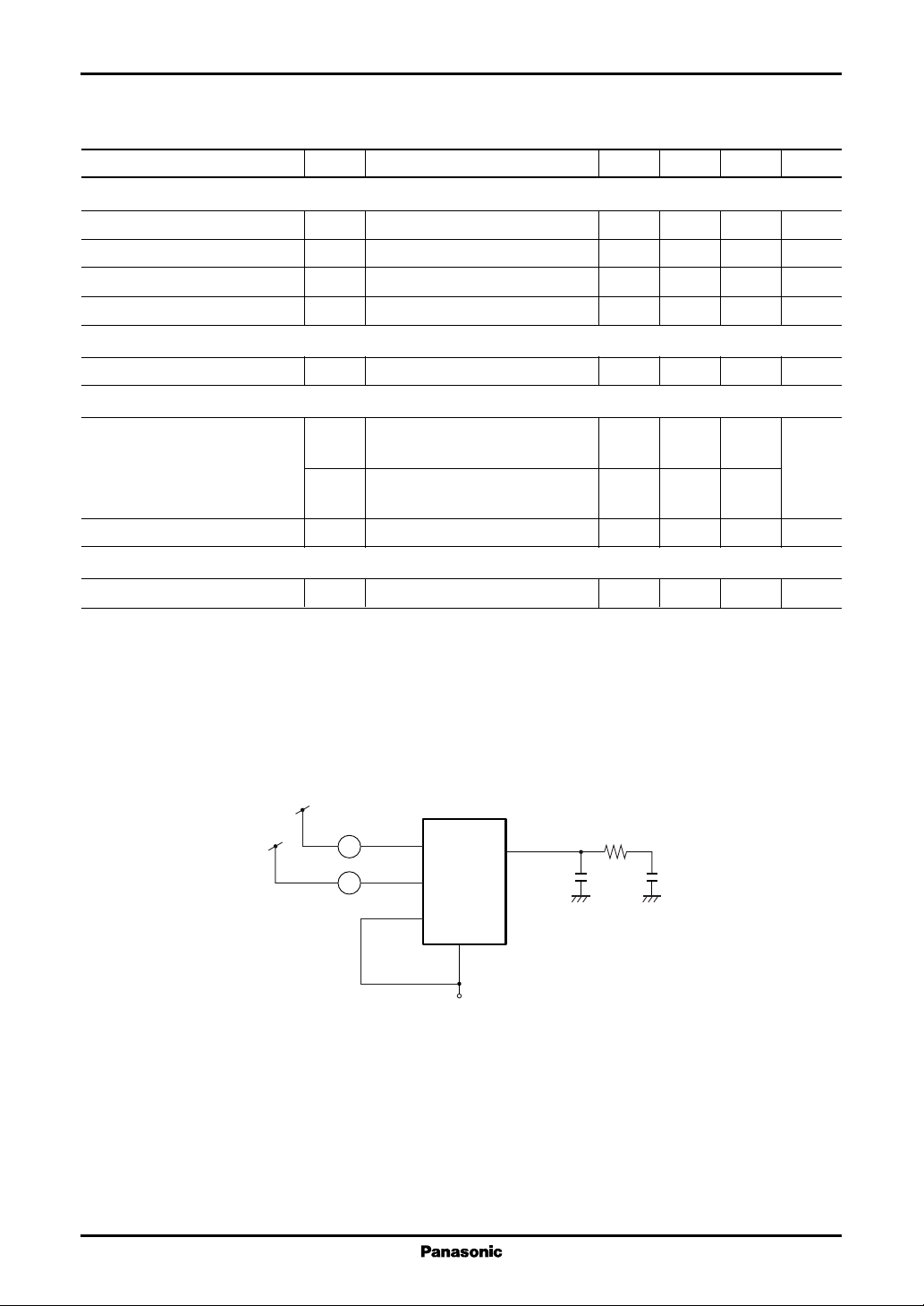
3. DC Characteristics at D
Parameter Symbol Conditions Min Typ Max Unit
3) Pull-down resistor pin TEST
High-level input voltage V
Low-level input voltage V
Input leakage current I
Pull-down resistance R
4) Reference voltage input pins VOPU, VOPL
Input current I
5) Analog output pins Y1 to Y384
4
Output current
*
Output voltage difference
6) Analog output pin (Y1 to Y384) output voltage range
Operating voltage range
Note) 1. *1: The standard conditions are as follows. A clock frequency of 50 MHz, a raster period of 15 µs, the data pattern
fixed at FF, the POL level switched between high and low at each raster period, INV1 and INV2 held fixed at the
low level, and each of VREF0 to VREF9 held fixed at its respective levels.
*2 : The maximum conditions are as follows. A clock frequency of 50 MHz, a raster period of 15 µs, the data pattern
switches between FF and 00 on each clock cycle, the POL level switched between high and low at each raster
period, INV1 and INV2 held fixed at the low level, and each of VREF0 to VREF9 held fixed at its respective levels.
*3: The loads on the analog output pins (Y1 to Y384) are shown below. The values of the components in the load
circuit are subject to change.
= 2.7 V to 3.6 V, A
VDD
5
*
*6
A
VDD
D
VDD
I
SS3
I
SS4
= 14.5 V to 15.5 V, A
VDD
IH3
IL3
LI3
PD
VOP
I
VOH
I
VOL
∆V
V
I
SS2
I
SS1
O
O
A
A
VX = 15 V, V
A
= 15 V, D
VDD
VX = 0.0 V, V
A
= 15 V, D
VDD
A
= 15 V, D
VDD
DUT
A
VDD
D
VDD
D
VSS
= 14 V, − 0.5 − 0.2 mA
OUT
VDD
OUT
VDD
VDD
= D
VSS
= 0 V, Ta = −20 °C to +75 °C (continued)
VSS
0.7 × D
0
VDD
D
0.3× D
VDD
VDD
−10 10 µA
40 100 350 kΩ
−100 100 µA
= 3.3 V
= 1.0 V, 0.2 0.5
= 3.3 V
= 3.3 V ±4 ±20 mV
A
+0.2
A
VDD
− 0.2
Y1
Y2
·
·
·
·
·
·
·
Y384
VSS
5 kΩ
75 pF
A
VSS
75 pF
A
VSS
V
V
V
VSS
A
0 V
DUT : Device Under Test
*4: The VX are the output voltages from the analog output pins Y1 to Y384.
The VOUT are the voltages applied to the analog output pins Y1 to Y384.
*5 : The standard conditions apply when the output voltages are at the same voltage as VOPL and VOPU.
*6 : Set up VREF0 to VREF9, VOPU, and VOPL so that the output voltages never exceed the output voltage range
listed above.
2. The following formula expresses the power dissipation when the loads described in *3 above are attached.
I
× A
+ I
SS1
VDD
SS3
× D
VDD
Replace ISS1 in the above formula with the value of ISS2 to calculate the power dissipation when there is no load.
3. The supply current in the no load state is provided for reference purposes and is not guaranteed.
23
Page 24
MN838850 Color TFT LCD Driver
■ Electrical Characteristics (continued)
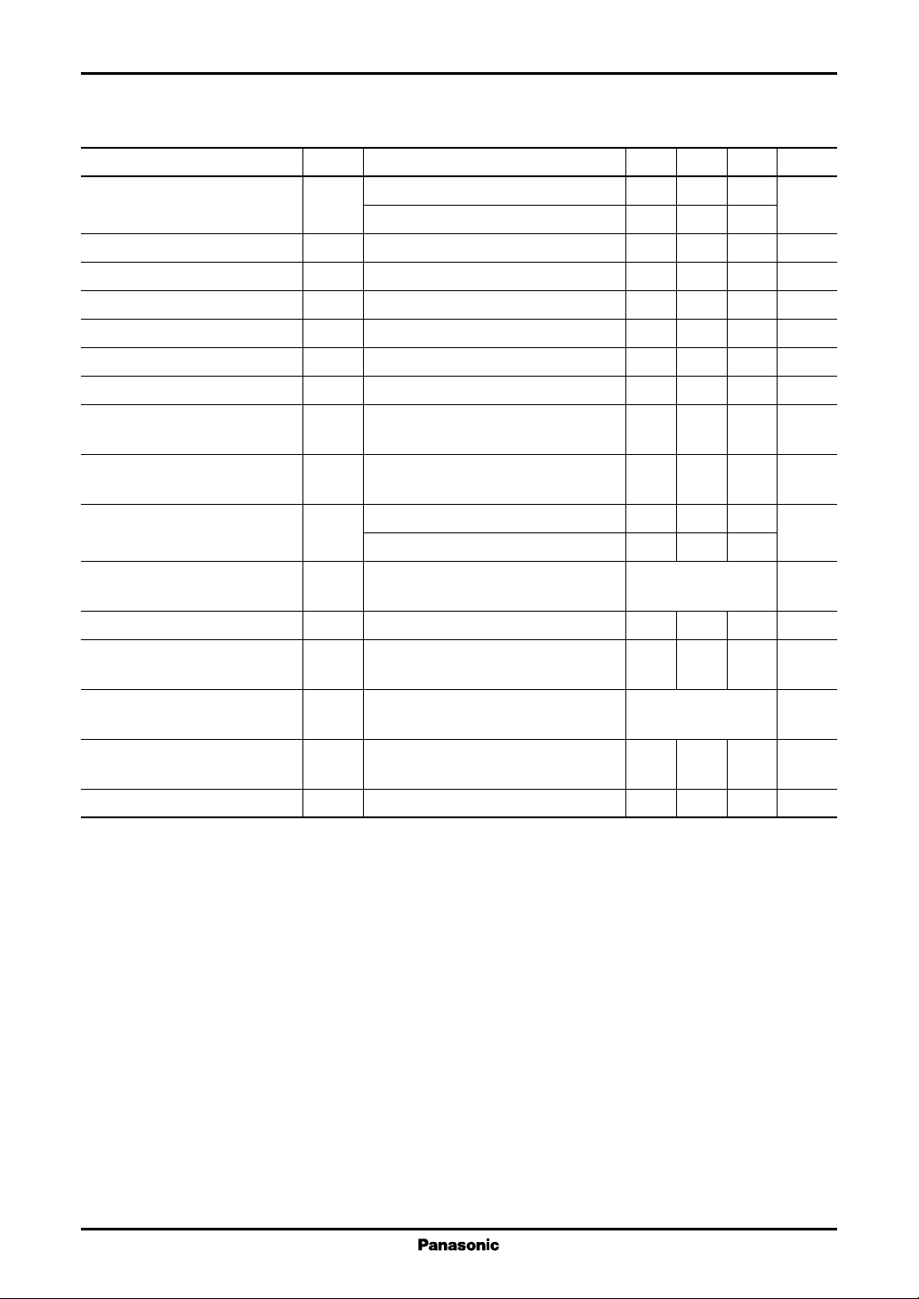
4. AC Characteristics at D
Parameter Symbol Conditions Min Typ Max Unit
FY period t
Clock high-level period t
Clock low-level period t
Data and INV setup time t
Data and INV hold time t
Start pulse setup time t
Start pulse hold time t
Start pulse low-level period t
Start pulse high-level period t
Carry signal delay time t
Carry signal rise time t
A signal low-level period t
A signal start pulse setup time
Data input invalid time
1
Last data timing
*
LCD drive signal delay time
Note) *1: The starting point is at the rise of the first clock cycle after the rise of the PRSL (PLSR) signal.
*2 : Stipulated as the value until the drive output voltage reaches the target output voltage ±20 mV (not including the
deviation).
*3: See note 1. *3 in section 3. DC Characteristics for the analog output pin load.
= 2.7 V to 3.6 V, A
VDD
1
*
1
*
2,3
*
wcH
wcL
hd1
hd2
wsL
wsH
wA
t
t
ng1
t
ng2
t
p
st1
st2
d1
c
st3
d2
= 14.5 V to 15.5 V, A
VDD
D
= 3.1 V to 3.6 V 20 ns
VDD
D
= 2.7 V to 3.6 V 25
VDD
VSS
= D
= 0 V, Ta = −20 °C to +75 °C (continued)
VSS
4 ns
4 ns
0 ns
4 ns
0 ns
4 ns
2 Clock
1 Clock
CL = 15 pF, D
CL = 15 pF, D
= 3.1 V to 3.6 V 13 ns
VDD
= 2.7 V to 3.6 V 17
VDD
64 Clock
2 µs
4 Clock
1 Clock
1 Clock
A
= 15 V 11 µs
VDD
cycles
cycles
cycles
cycles
cycles
cycles
24
Page 25
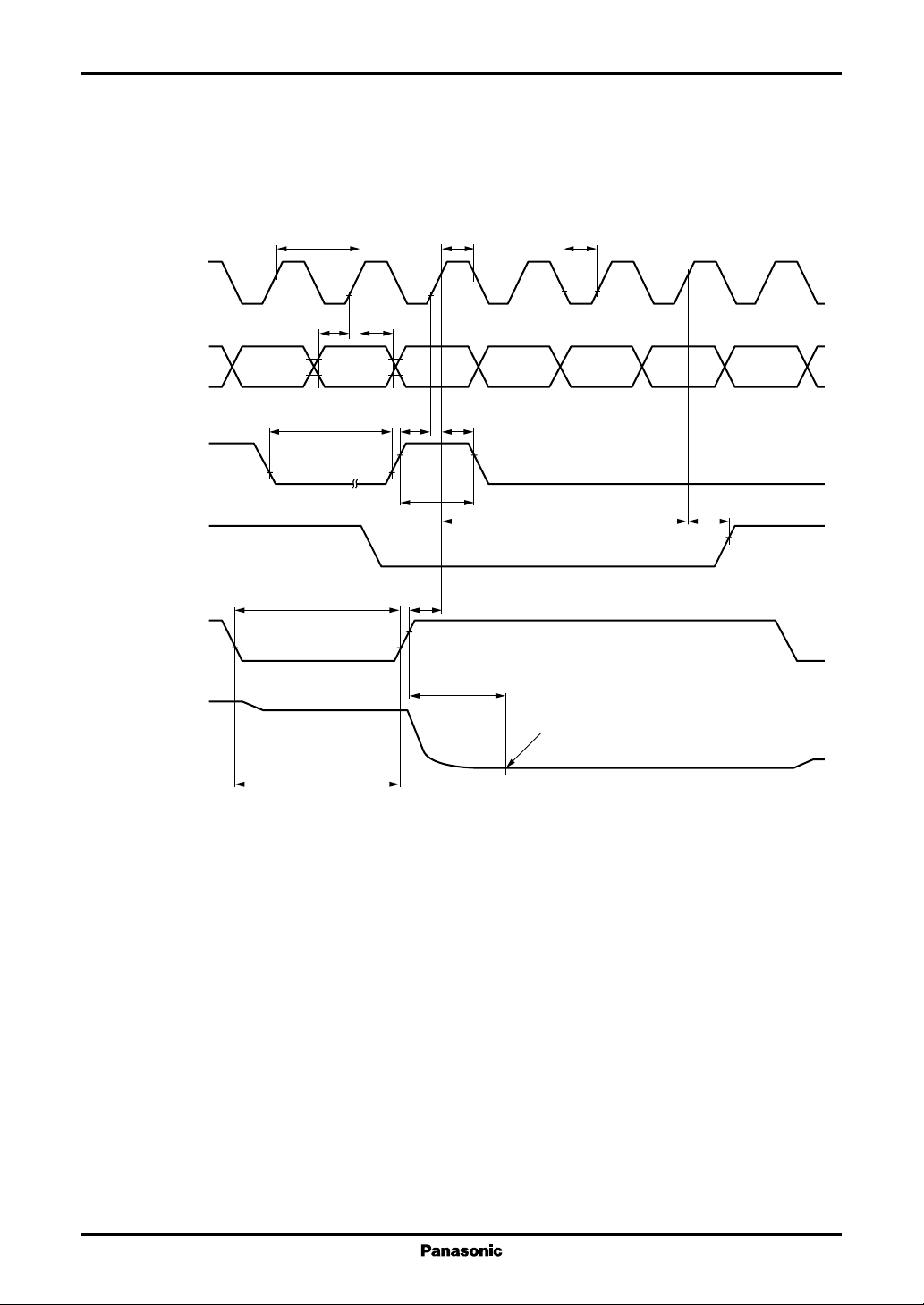
Color TFT LCD Driver MN838850
■ Electrical Characteristics (continued)
4. AC Characteristics (continued)
FY
Dxx
INV1
INV2
Input
PLSR(RL = "H")
PRSL(RL = "L")
Output
PRSL(RL = "H")
PLSR(RL = "L")
A signal
Y1 to Y384
t
p
V
IH
t
t
hd1
st
t
wsL
t
wA
Hi-Z
D/A converter setup period
t
t
st2thd2
t
wsH
t
st3
wcH
t
d2
t
wcL
V
IL
t
c
t
d1
Target output voltage ±20 mV
(not including the deviation)
Target output voltage
V
OH
Hi-Z
The D/A converter setup period (when the outputs are high impedance) is synchronized
with the falling edge of the A signal.
Unless otherwise specified, the digital input and output levels are
V
= VOH 0.7 × D
IH
, VIL = VOL = 0.3 × D
VDD
VDD
.
25
Page 26
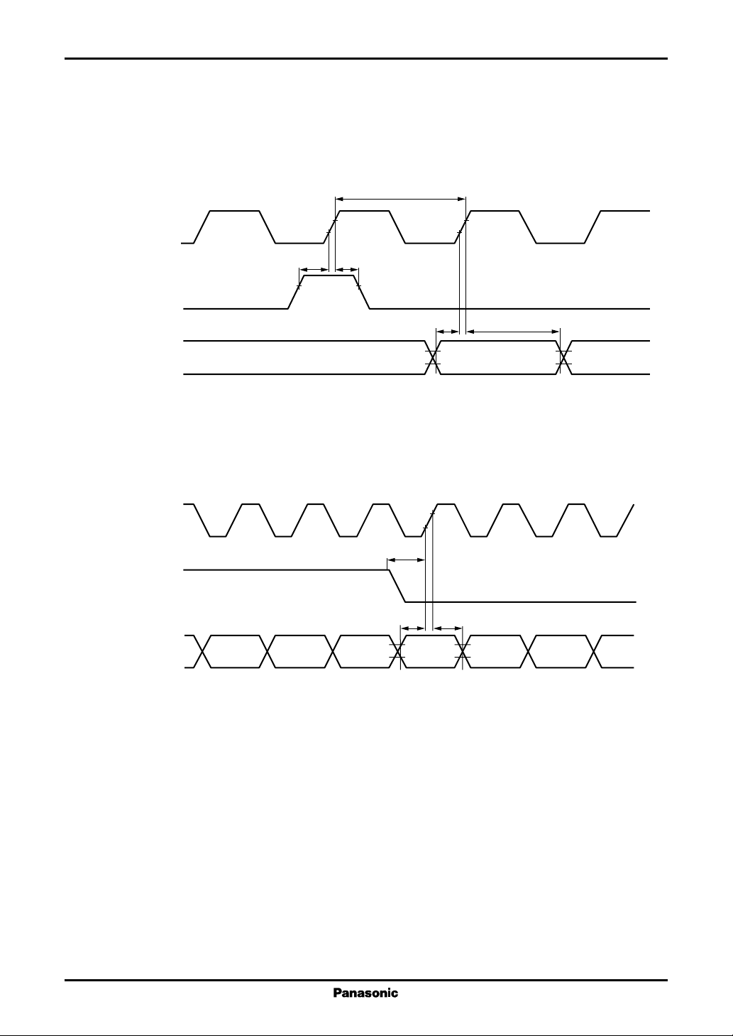
MN838850 Color TFT LCD Driver
■ Electrical Characteristics (continued)
4. AC Characteristics (continued)
t
ng1
FY
t
st2thd2
Input
PLSR(RL = "H")
PRSL(RL = "L")
Dxx
INV1
INV2
t
st1
t
hd1
FY
A singal
Dxx
INV1
INV2
Valid
t
ng2
t
st1thd1
Valid Valid Valid
Invalid
Invalid Invalid
26
 Loading...