

Page 1
A/D, D/C Converters for Image Signal Processing
MN65742
6-Bit, 2-Channel CMOS A/D Conv erter
Overview
The MN65742 is a 6-bit, 2-channel CMOS analog-todigital converter. It uses a totally parallel structure based
on differential comparators to achiev e high-speed operation.
Features
Resolution: 6 bits
Maximum conversion rate: 60 MSPS (min.)
Linearity error: ±1.3 LSB (typ.)
Differential linearity error: ±1.3 LSB (typ.)
Analog input voltage level:
1.5 V
(typ.) (1.0 to 2.5 V)
p-p
Power supply voltage: 5.0 ±0.25 V
3.0 to 5.25 V (power supply for output pins)
Power consumption: 250 mW (typ.) (FC= 60 MSPS,
not including reference current)
Applications
Digital satellite broadcasting receivers
Digital video equipment
Multimedia equipment
Communications equipment
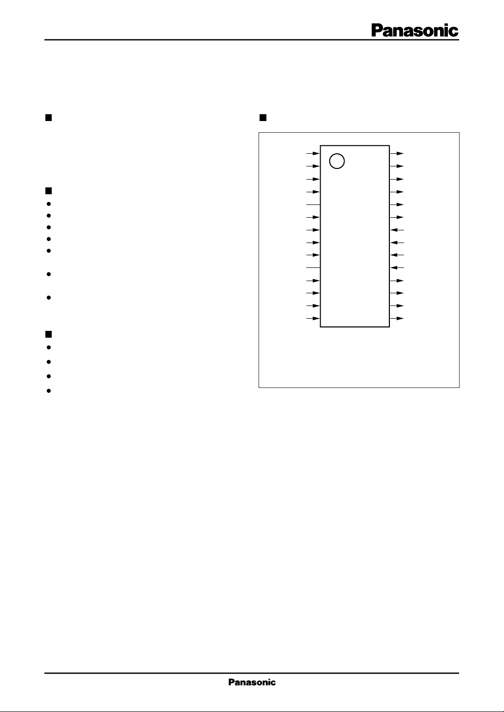
Pin Assignment
DD
DD
DD
1
2
3
SS
4
5
6
7
SS
8
9
10
11
12
13
SS
14
SOP028-P-0375
CLK
AV
AV
VRT
N.C.
VINA
AV
AV
POWD
VRM
V
INB
VRB
AV
AV
(TOP VIEW)
28
DA5
27
DA4
26
DA3
25
DA2
24
DA1
23
DA0
22
AV
SS
21
AV
DDL
20
DB5
19
DB4
18
DB3
17
DB2
16
DB1
15
DB0
1
Page 2
MN65742 A/D, D/C Converters for Image Signal Processing
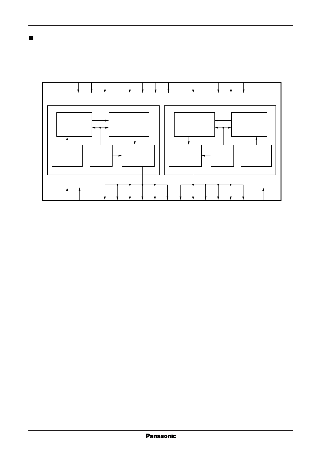
Block Diagram
AVDDAVDDAV
2
8
DD
AVSSAVSSAVSSAV
3
14
7
SS
13
22
RT
V
VRM
4
10
VRBV
12
INAVINB
6
Channel B (Bch.) Channel A (Ach.)
Comparator Comparator
Reference
resistor array
9
POWD
Clock
generator
1
CLK
Encoder Encoder
Output logic
circuits
15
16
17
18
19
DB0
DB1
DB2
DB3
DB4
Output logic
circuits
20
23
DB5
DA0
24
DA1
25
DA2
Clock
generator
26
DA3
27
28
DA4
11
Reference
resistor array
DA5
N.C.
5
21
DDL
AV
2
Page 3
A/D, D/C Converters for Image Signal Processing MN65742
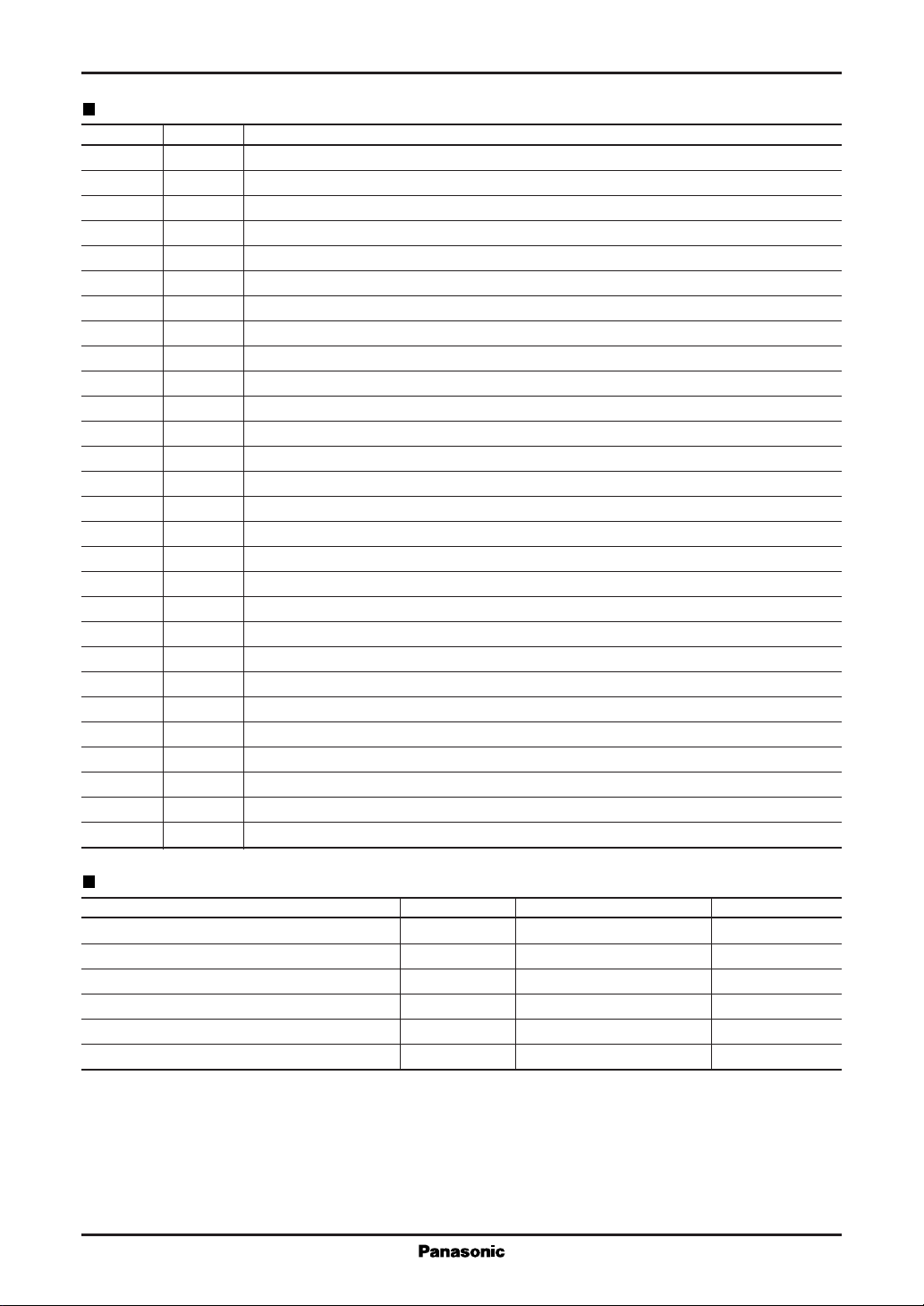
Pin Descriptions
Pin No. Symbol Function Descriptions
1 CLK Clock input
2AVDDPower supply for analog circuits
3AVSSGround for analog circuits
4VRTReference voltage (top)
5 N.C. No connection
6V
INA
7AVSSGround for analog circuits
8AVDDPower supply for analog circuits
9 POWD Power-down selection pin
10 VRM Intermediate reference voltage
11 V
12 V
13 AV
14 AV
INB
RB
SS
DD
15 DB0 Digital output pin
16 DB1 Digital output pin
17 DB2 Digital output pin
18 DB3 Digital output pin
19 DB4 Digital output pin
20 DB5 Digital output pin
21 AV
22 AV
DDL
SS
23 DA0 Digital output pin
24 DA1 Digital output pin
25 DA2 Digital output pin
26 DA3 Digital output pin
27 DA4 Digital output pin
28 DA5 Digital output pin
Analog signal input pin
Analog signal input pin
Reference voltage (bottom)
Ground for analog circuits
Power supply for analog circuits
Power supply pin for digital output circuits
Ground for analog circuits
Absolute Maximum Ratings Ta=25˚C
Parameter Symbol Rating Unit
Power supply voltage AV
Power supply voltage for output circuits AV
Input voltage V
Output voltage V
Operating ambient temperature T
Storage temperature T
DD
DDL
I
O
opr
stg
– 0.3 to +7.0 V
– 0.3 to AV
– 0.3 to AV
– 0.3 to AV
+0.3 V
DD
+0.3 V
DD
+0.3 V
DD
–20 to +70 ˚C
–55 to +125 ˚C
3
Page 4
MN65742 A/D, D/C Converters for Image Signal Processing
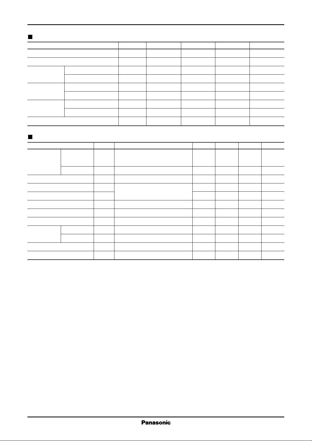
Recommended Operating Conditions AV
=5.0V, AV
DD
=3.3V, AVSS=0V, T a=25˚C
DDL
Parameter Symbol min typ max Unit
Power supply voltage V
Power supply voltage for digital outputs DV
Digital input "H" level V
voltage "L" level V
Reference "H" level V
voltage "L" level V
Clock "H" level pulse width t
"L" level pulse width t
Analog input voltage V
Electrical Characteristics AV
=5.0V, AV
DD
DD
DDL
IH
IL
RT
RB
WH
WL
AIN
DDL
4.75 5.00 5.25 V
3.00 3.30 5.25 V
2.2 AV
AV
SS
DD
0.8 V
V
2.0 2.5 3.5 V
0.5 1.0 2.0 V
7ns
7ns
AV
SS
=3.3V, AVSS=0V , VRT=2.5V, VRB=1.0V, Ta=25˚C
AV
DD
V
Parameter Symbol Conditions min typ max Unit
Current AV
DD
consumption (not including reference current)
AV
DDL
I
DDfCLK
I
DDL
= 60 MSPS
47 80 mA
36mA
Resolution RES 6 bit
Linearity error E
Differential linearity error E
Maximum conversion rate F
C(max.)
Clock frequency f
Analog input dynamic range D
Output "H" level I
current "L" level I
Output delay time t
Analog input capacitance C
L
f
=60MSPS
CLK
D
60 MSPS
CLK
R
VOH=DV
OH
VOL=0.4V 2.0 mA
OL
CL=20pF 3 7 11 ns
d
I
– 0.8V –2.0 mA
DDL
1 60 MHz
1.4 VRT–V
±0.7 ±1.3 LSB
±0.7 ±1.3 LSB
V
RB
20 pF
4
Page 5
A/D, D/C Converters for Image Signal Processing MN65742
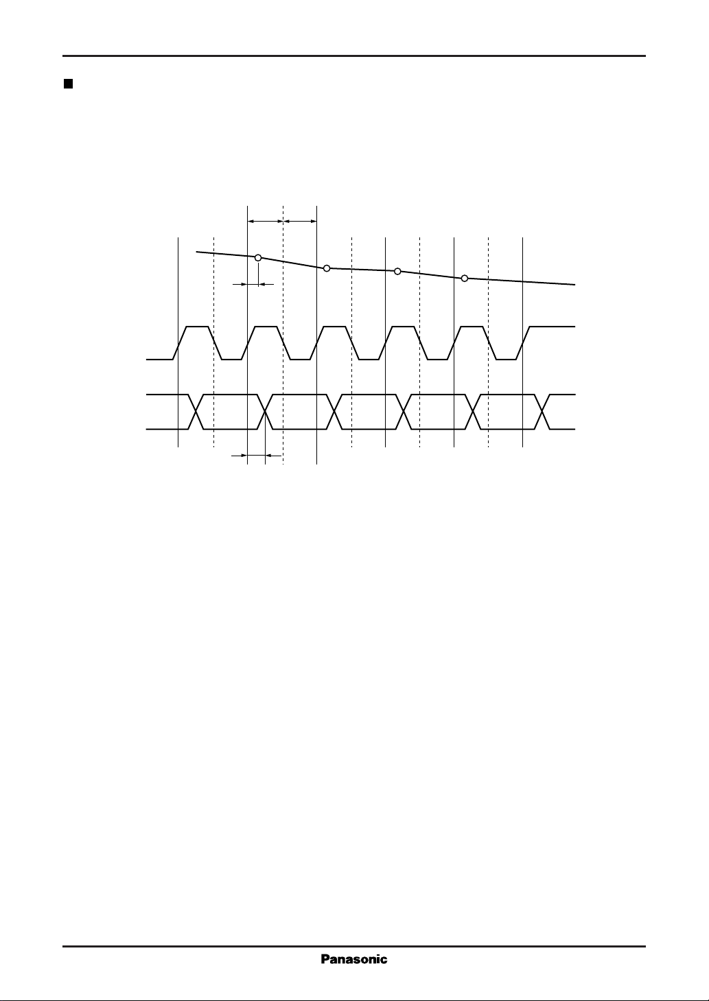
Timing Chart
The chip samples the analog input at the rising edge of the clock signal and provides the corresponding digital
output one clock cycle later at the rising edge of the clock signal.
t
WHtWL
Analog input
N
t
sd
Clock
Data output
Note: The circles indicate analog signal sampling points.
N-1
t
d
N+1
N+2
N+3
1.5V
N
N+1 N+2 N+3
1.5VN-2
5
Page 6
MN65742 A/D, D/C Converters for Image Signal Processing
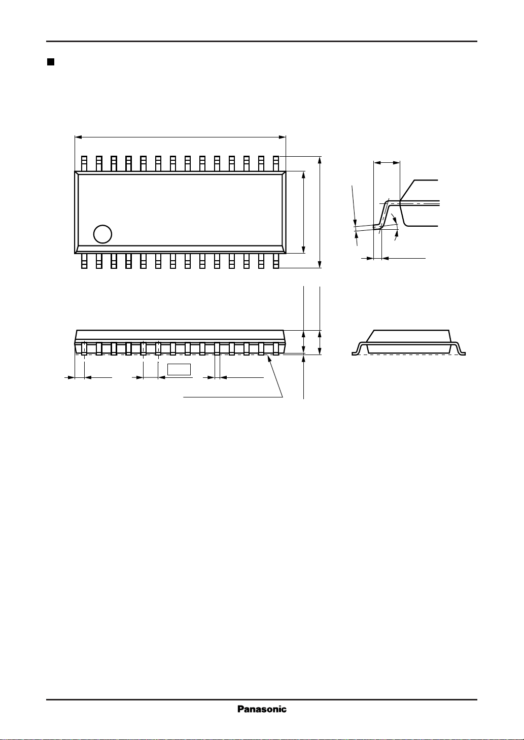
Package Dimensions (Unit:mm)
SOP028-P-0375
±0.20
17.80
28
15
0.05
-
+0.10
1.10±0.20
0.15
7.20±0.202.00±0.200.10±0.10
0 to 10°
0.30min.
114
2.40max. 9.40±0.30
(0.65) 0.40
1.27
±0.10
SEATING PLANE
6
 Loading...