

Page 1
For Communications Equipment
MN86062
CODEC LSI for Facsimile Images
Overview
The MN86062 is a high-speed LSI codec for compressing
and decompressing images using the MH, MR, and MMR
standard compression methods specified in the ITU-T T.4
and T.6 recommendation. Registers and other settings
provide flexible support for a variety of processing.
Features
Compression methods
MH, MR, and MMR
Operating mode:
Page mode
Bus configuration:
Choice of dual- or single-bus operation
Decoding error processing:
Choice of replacing with the previous line or a
white line
Image bus configuration:
8 bits, maximum 16 megabytes address
space of image bus, 2-channel master DMA
System bus configuration:
X80 interface compatible, 8 bits, 2-channel
slave DMA
Pixels per line:
maximum 64K, in byte increments
Concurrent DMA transfers over image bus and
command processing
Support for pointer management for image buffer
Wide selection of independent parameters for coding,
decoding, transfers between buses, and DMA
transfersr
Support for time-shared processing by line for both
coding and decoding
Applications
Facsimile equipment
Page 2
MN86062 For Communications Equipment
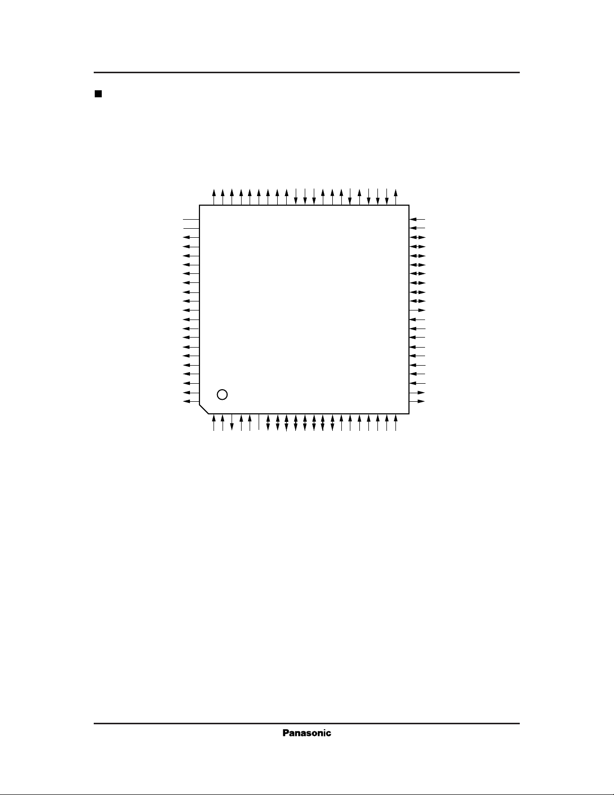
Pin Assignment
N.C.1
N.C.2
IA18
IA17
IA16
IA15
IA14
IA13
IA12
IA11
IA10
IA9
IA8
IA7
IA6
IA5
IA4
IA3
IA2
IA1
IA0
IA19
IA20
IA21
IA22
IA23
NDCMP
NDEND
NDACK1
NDACK0
NDREQ1
NDREQ0
NIDACK
IR/W
NIAEN
NDRUN
NIBACK
NIBREQ
2SYSCLK
636261605958575655545352515049484746454443
64
65
66
67
68
69
70
71
72
73
74
75
76
77
78
79
80
81
82
83
84
123456789101112131415161718192021
SS2
SS3
DD2
DD3
ID7
ID6
ID5
ID4
ID3
V
V
V
V
N.C.3
TACK
ID2
ID1
ID0
V
DD4
SS4
V
TEST2
TEST1
DD1VSS1
V
TEST0
NACKD
SYSCLK
42
41
40
39
38
37
36
35
34
33
32
31
30
29
28
27
26
25
24
23
22
NACKC
TEST3
TEST4
D0
D1
D2
D3
D4
D5
D6
D7
NIRQ
NRESET
A0
A1
A2
A3
NCS
NRD
NWT
NREQC
NREQD
(TOP VIEW)
QFP084-P-1818
Page 3
For Communications Equipment MN86062
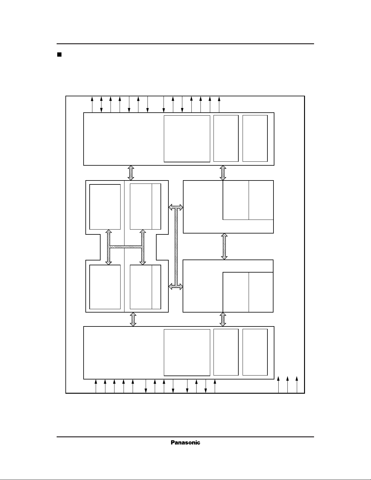
Block Diagram
IA(23:0)
ID(7:0)
IR/W
NIAEN
NIDACK
NIBREQ
NIBACK
51
50
52
Image bus interface
Sub sequencer
NDREQ0
47
48
53
Parameter register
NDACK0
55
54
NDREQ1
NDACK1
NDRUN
56
49
Master DMA
(2 channels)
NDEND
NDCMP
57
58
Reference line FIFO
Change point
detector
Mode selection block
Coding line FIFO
Image
reconstruction
block
Microprogram control block
Main sequencer
System bus
interface
25
NCS
A(3:0)
D(7:0)
NRD
24
NWT
ALU1 ALU2
32
NIRQ
Register bank
314643
NRESET
2SYSCLK
Slave DMA
23
SYSCLK
Table look-up block
(2 channels)
21
22
NREQC
NACKC
20
NREQD
NACKD
Coding table
Coding FIFO
Decoding table
Decoding FIFO
DD
V
SS
V
TEST(4:0)
Page 4
MN86062 For Communications Equipment
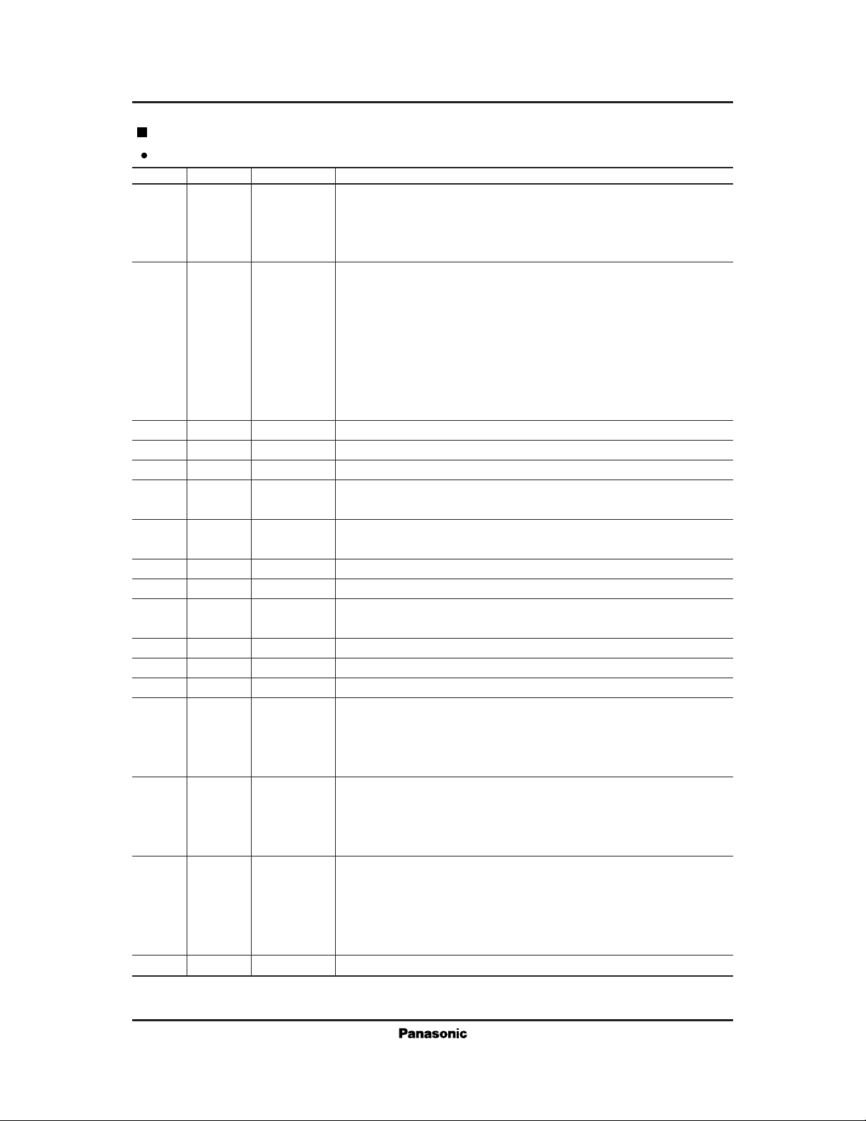
Pin Descriptions
System Bus Interface
Pin No. Symbol I/O Function Description
27 A3 I Address bus for accessing internal registers
28 A2
29 A1
30 A0
33 D7 I/O Data bus for bidirectional transfers over system bus
34 D6 Tristate
35 D5
36 D4
37 D3
38 D2
39 D1
40 D0
24 NWT I Connect to WR pin on X80-compatible microprocessor
25 NRD I Connect to RD pin on X80-compatible microprocessor
26 NCS I Chip select pin
23 NREQC O This output pin indicates a DMA transfer request from the 86062 to
Tristate memory.
22 NREQD O This output pin indicates a DMA transfer request from the memory to
Tristate 86062.
21 NACKC I This input pin accepts the response to the NREQC signal.
20 NACKD I This input pin accepts the response to the NREQD signal.
32 NIRQ O
Open drain
31 NRESET I External input resets the 86062.
46 2SYSCLK I This input pin accepts a clock signal with twice the system clock frequency.
43 SYSCLK O This output pin provides a clock signal with half the frequency of 2SYSCLK.
15 V
5V
2V
45 V
16 V
4V
1V
44 V
DD4
DD3
DD2
DD1
SS4
SS3
SS2
SS1
I Connect these power supply pins to a 5 volt power supply.
I Connect these power supply pins to ground.
41 TEST4 I Do not use these test pins.
42 TEST3
17 TEST2
18 TEST1
19 TEST0
3 TACK O Do not use these test pins.
This output pin indicates an interrupt request.
Page 5
For Communications Equipment MN86062
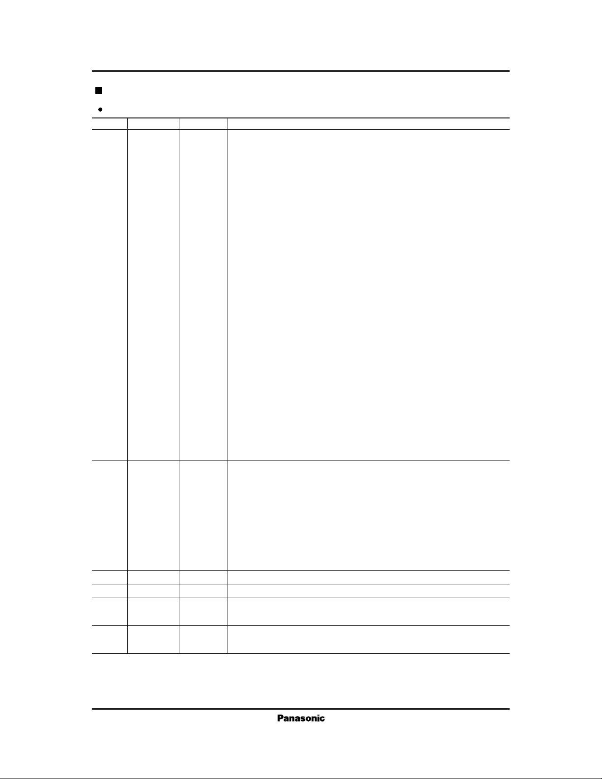
Pin Descriptions (continued)
Image Bus Interface (continued)
Pin No. Symbol I/O Function Description
59 IA23 O Image address bus. The address is valid when the NIAEN pin is at "L"
60 IA22 Tristate level.
61 IA21
62 IA20
63 IA19
66 IA18
67 IA17
68 IA16
69 IA15
70 IA14
71 IA13
72 IA12
73 IA11
74 IA10
75 IA9
76 IA8
77 IA7
78 IA6
79 IA5
80 IA4
81 IA3
82 IA2
83 IA1
84 IA0
7 ID7 I/O Image data bus for bidirectional transfers of image data
8 ID6 Tristate
9 ID5
10 ID4
11 ID3
12 ID2
13 ID1
14 ID0
47 IBREQ O This output pin indicates a request for control of the image bus.
48 IBACK I This input pin accepts the response to the NIBREQ signal.
50 IAEN O This output pin indicates whether the values of image address bus are
Tristate valid.
51 IR/W O This output pin indicates the data transfer direction for the image bus.
Tristate
Page 6
MN86062 For Communications Equipment
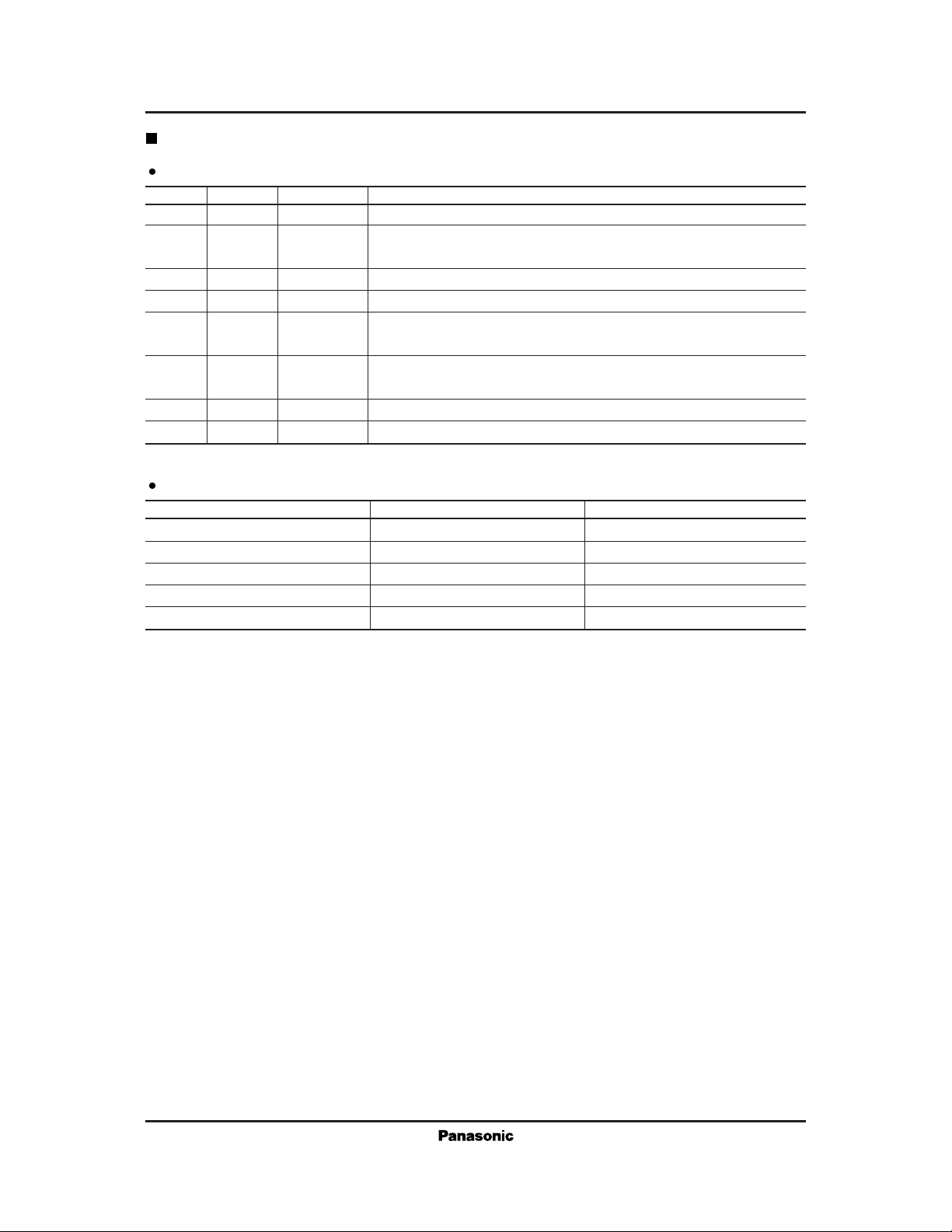
Pin Descriptions (continued)
Image Bus Interface (continued)
Pin No. Symbol I/O Function Description
52 IDACK I This input pin indicates the end of a data read or write operation.
49 DRUN O This output pin indicates whether a DMA transfer is in progress.
Tristate
57 DEND O This output pin indicates the end of a DMA cycle.
58 DCMP O This output pin indicates successful completion of a DMA block transfer.
53 DREQ0 I This input pin indicates a DMA transfer request from the I/O block to
memory.
54 DREQ1 I This input pin indicates a DMA transfer request from the memory to
I/O block.
55 DACK0 O This output pin gives the response to the NDREQ0 signal.
56 DACK1 O This output pin gives the response to the NDREQ1 signal.
Test Pin Setting
Symbol Pin No. Fixed Level
TEST0 19 GND
TEST1 18 GND
TEST2 17 GND
TEST3 42 GND
TEST4 41 GND
Page 7
For Communications Equipment MN86062
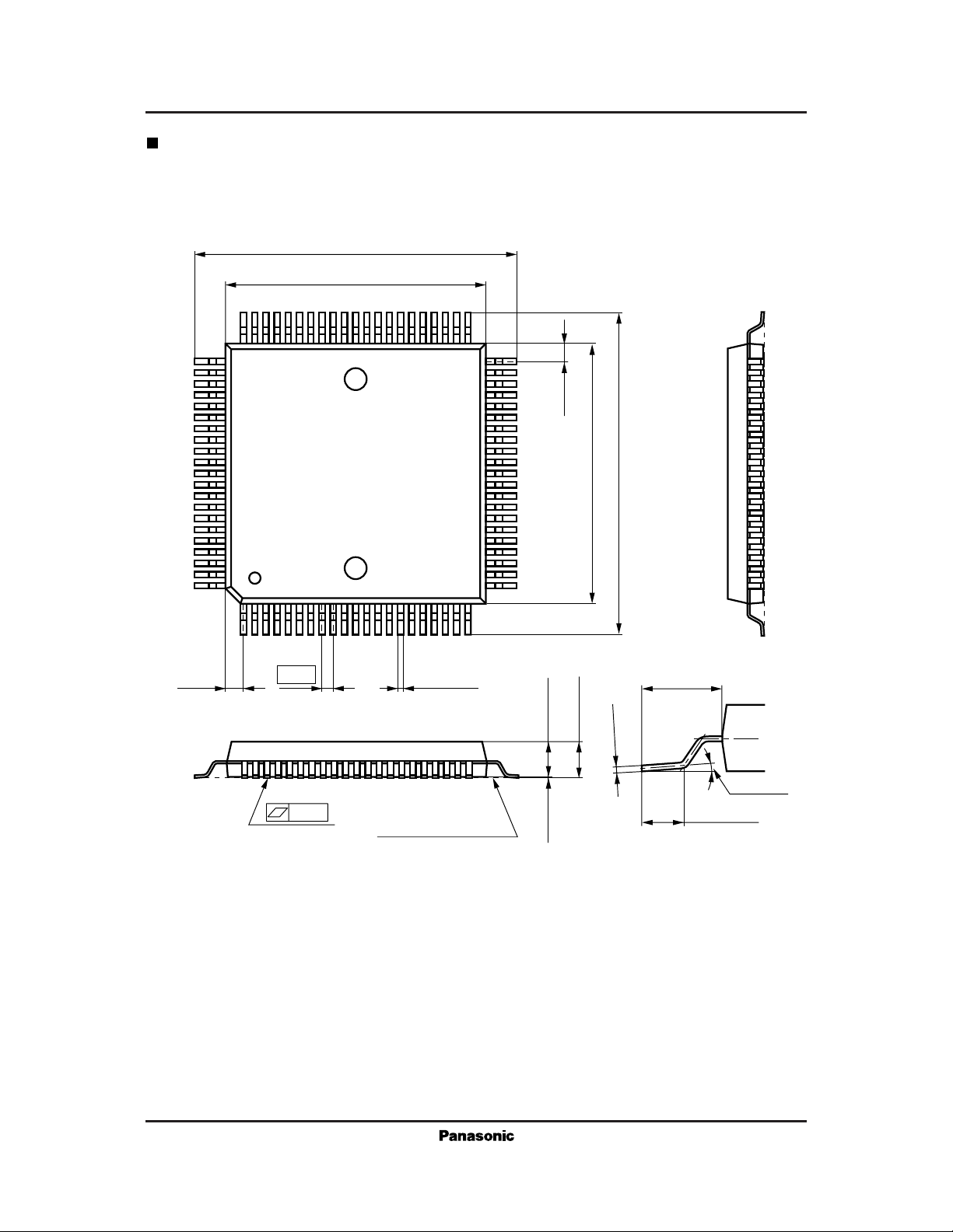
Package Dimensions (Unit: mm)
QFP084-P-1818
22.90±0.40
18.00±0.20
63 43
64
84
(1.00)
42
(1.00)
18.00±0.20
22.90±0.40
22
121
0.80
0.35±0.10
2.50±0.20
2.90 max.
0.05
-
+0.10
(2.45
0.15
±0.20)
0 to 10°
0.15
SEATING PLANE
0.10±0.10
(1.30
±0.20)
 Loading...