

Page 1
EEPROMs
MN63121
1K-Bit EEPROM
Overview
The MN63121 is a 1K-bit EEPROM supporting serial
I/O and operating on a single power supply with a voltage between 1.8 and 5.5 V. It provides the following pins
for easy interfacing to microprocessors or
microcontrollers: chip select (CS), serial clock (SCK),
data input (DI), data output (DO), reset (RESET), and
busy (RDY/BUSY). It includes a built-in timer for use in
automatically erasing and writing data during data update operations.
The memory organization is 64 × 16 bits. The chip indicates the end of a write operation with either the RDY/
BUSY pin or the state of the DO pin after the status output mode has been set.
Conversion of peripheral circuits to CMOS realizes
great reductions in power consumption. Use of floating
gate memory cells and a built-in error correction circuit
ensures reliable operation for 10
5
write cycles.
Features
Memory organization: 64 × 16 bits
Floating gate memory cells
Function blocking erroneous writes
Low power consumption
- Reads: max. 6.6 mW for V
- Standby: max. 66 µW for V
Built-in self-timer for use in automatically erasing
and writing
Built-in error correction circuit that guarantees 10
write cycles
10-year data preservation period
= 3.3 V
CC
= 3.3 V
CC
5
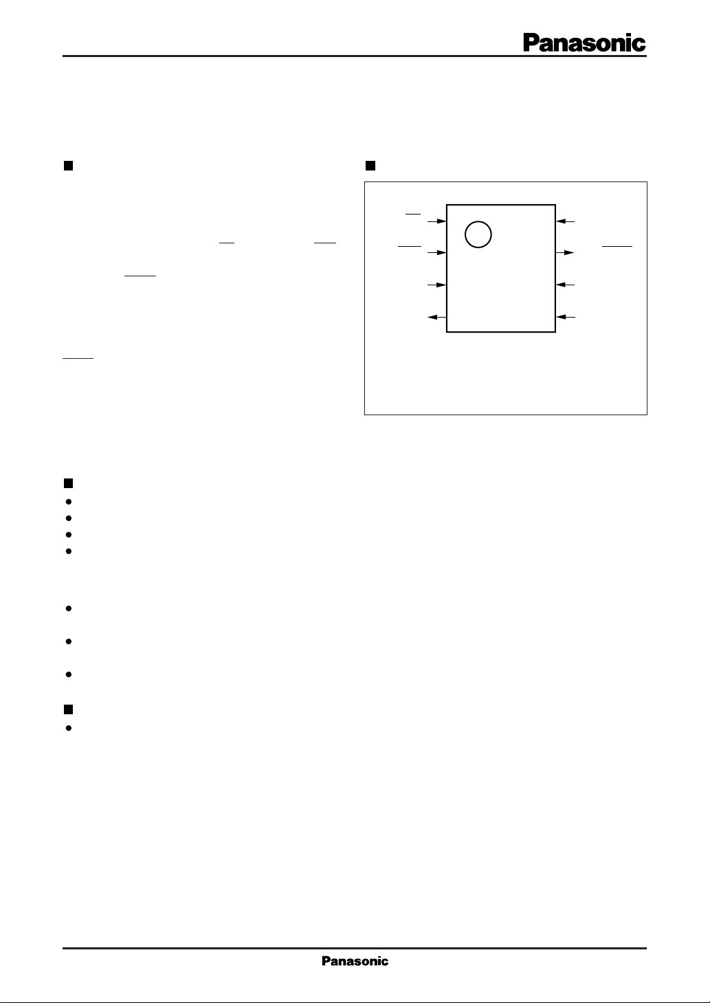
Pin Assignment
DI
1
2
3
4
( TOP VIEW )
DIP008-P-0300A
CS
SCK
DO
8
7
6
5
V
CC
RDY/BUSY
RESET
GND
Applications
Keyless entry systems, cordless telephones, storage
for recognition and adjustment data for terminals,
etc.
1
Page 2
MN63121 EEPROMs
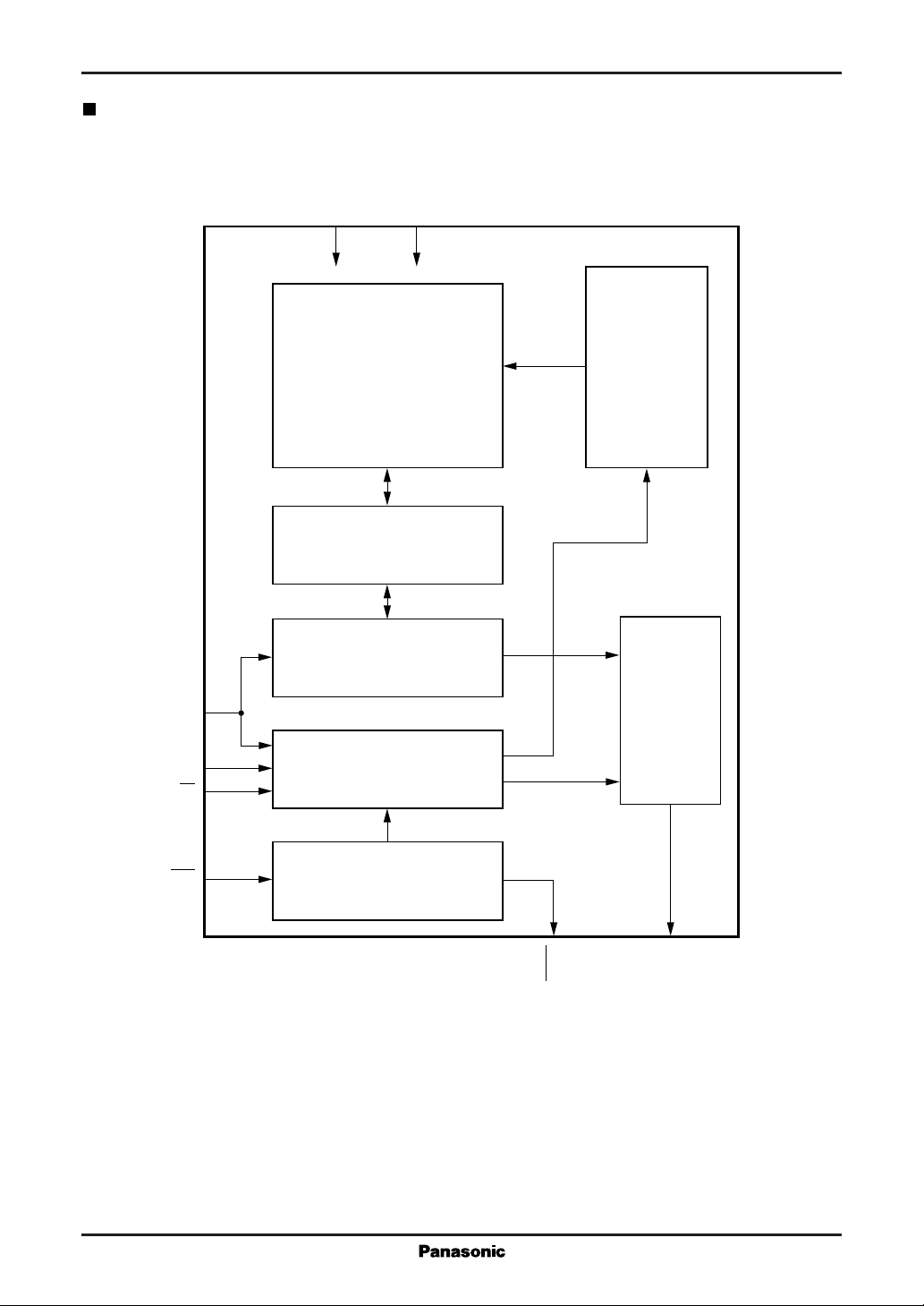
Block Diagram
CC
V
8
GND
5
DI
RESET
CS
SCK
Memory array
64 × 16
Error correction circuit
Data register
3
6
1
2
Mode decode logic
Clock generator
Address decoder
Output
buffer
7
RDY/BUSY
4
DO
2
Page 3
EEPROMs MN63121
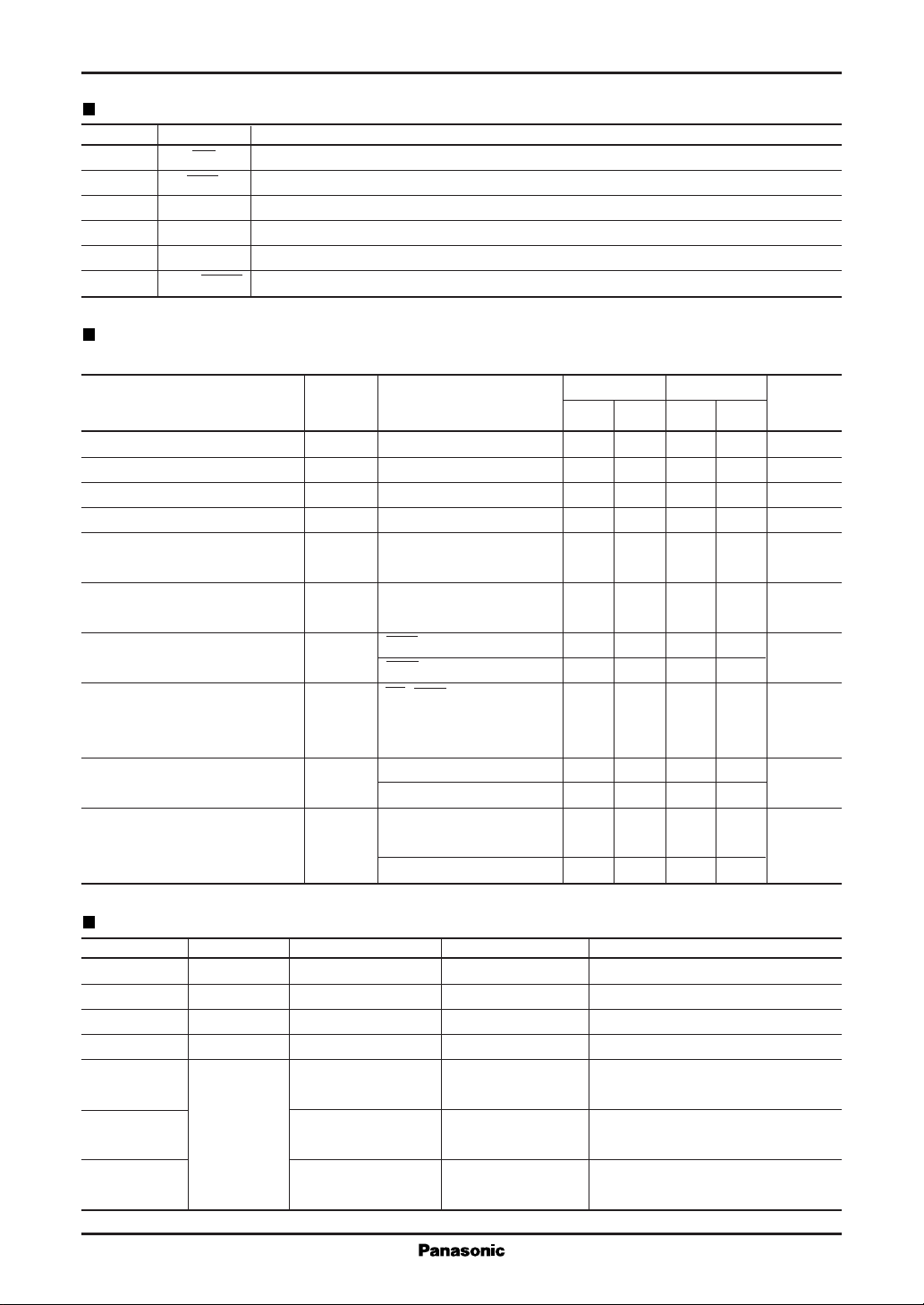
Pin Descriptions
Pin No. Symbol Pin Name
1 CS Chip select input
2 SCK Serial clock input
3 DI Data input
4 DO Data output
6 RESET Reset input
7 RDY/BUSY Busy output
Electrical Characteristics
VCC=1.8 to 5.5V, Ta=–10˚C to +70˚C
Parameter Symbol Test Conditions
Power supply voltage V
Input leakage current at "L" level I
Input leakage current at "H" level I
Output leakage current I
Input voltage at "L" level V
Input voltage at "H" level V
VCC power supply current I
CC
LIL
LIH
LO
IL
IH
SCK=250kHz — 2.0 — —
CC
(during operation) SCK=1MHz — — — 3.0
power supply current I
V
CC
CS, SCK, DI, — 20 — 30 µA
SB
(during standby) RESET="H"
Other pins open
Output voltage for "L" level
(during reads) IOL=2.1mA — — — 0.45
V
Output voltage for "H" level
(during reads) V
IOL=400 µA — 0.3 — — V
OL
=–10 µA
I
OH
OH
IOH=–400 µA — — 2.4 —
2 to 3 V Operation 5 V Operation
min max min max
1.8 3.3 4.5 5.5 V
–10 10 –10 10 µA
–10 10 –10 10 µA
—10—10 µA
0.2 ×
– 0.1
0.8 × V
V
CC
V
CC
– 0.3
– 0.1 0.7 V
V
CC
3.0
V
CC
CC
+0.3 +0.3
———
Unit
V
mA
V
Function Descriptions
Orders Code Address Data Function
READ 10101000 A0A1A2A3A4A500 D0 –D7D8–D
WRITE 10100100 A0A1A2A3A4A500 D0 –D7D8–D
15
15
EWEN 10100011 xxxxxxxx –––– Enable erase/write
EWDS 10100000 xxxxxxxx –––– Disable erase/write
BUSYFG 00xxxxxx 0(busy) Status output busy flag
1(ready)
ENFG
10101001
10xxxxxx 0(enable) Status output write enable flag
1(disable)
ECCFG 01xxxxxx 0(non-correction) Status output ECC flag
1(correction)
Note: x means "don't care".
Read from address indicated with pins A0 –A
Write to address indicated with pins A0 –A
5
5
3
Page 4
MN63121 EEPROMs
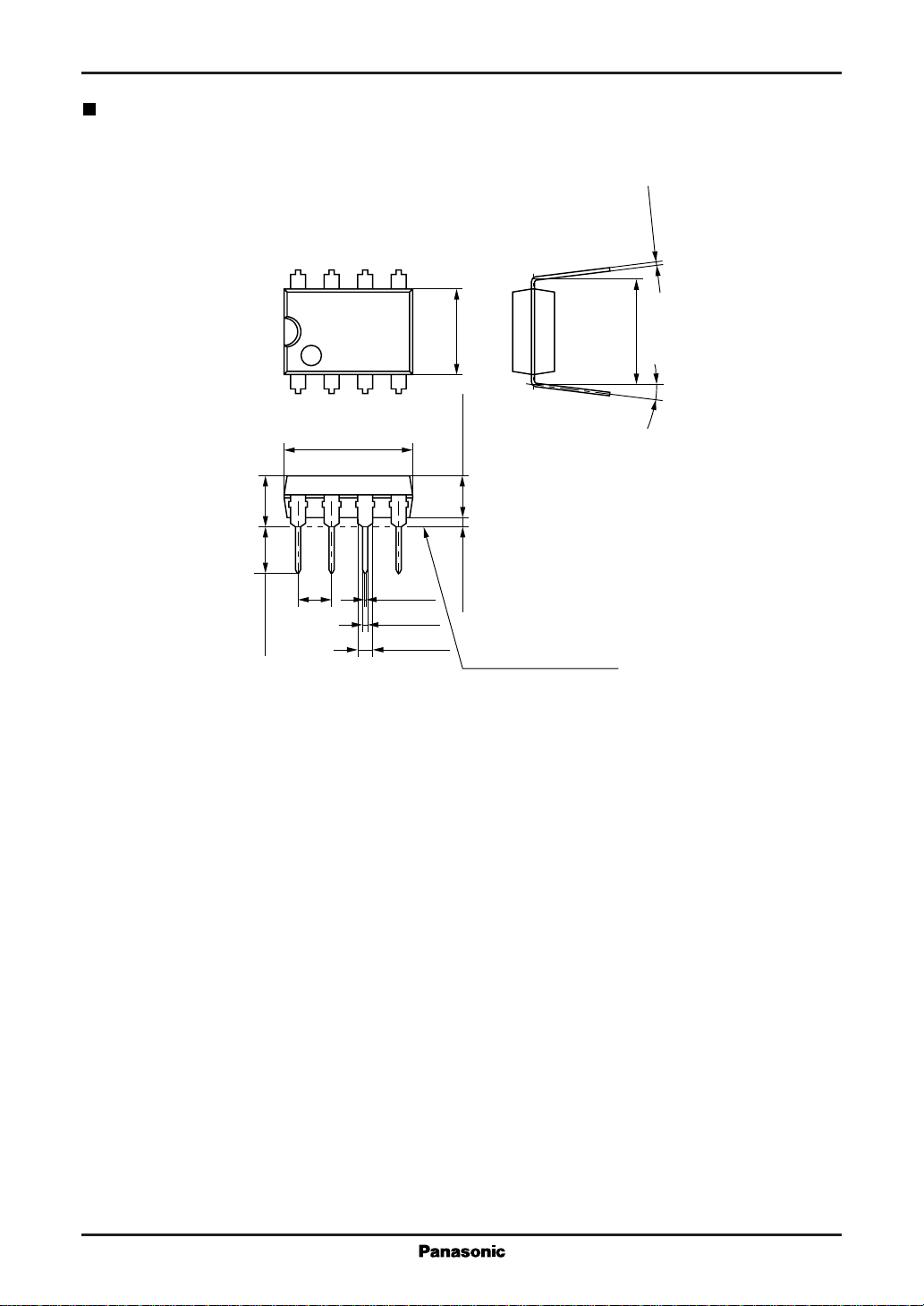
Package Dimensions (Unit:mm)
DIP008-P-0300A
–0.05
+0.20
85
14
9.60±0.40
4.80 max.
2.54
3.45±0.30
0.50±0.10
0.70±0.10
1.30±0.10
6.40±0.20
3.30±0.20
0.70 min.
SEATING PLANE
0.25
0° to 15°
7.62±0.20
4
 Loading...