

Page 1
For Communications Equipment
MN86074
Image Processing LSI
Overview
The MN86074 boosts image quality by applying various
image processing techniques to the analog signal from
an image sensor. Features include correction of laser
printer dot spreading at the pixel level, processing to
enhance the compression ratio, reproduction of halftone
images with 64-gradation, two-dimensional MTF
correction using moire suppression, and infinite shading
for all pixels using a division technique. These combine
to yield top image reproduction quality.
Features
Image processing that yields top image quality
• Infinite shading for all pixels using a division technique
• Error dispersion processing that reproduces halftone
images with 64-gradation
User-programmable gamma curve
• Two dimensional MTF correction
• High-quality reduction with a user-specified scaling
factor
Preserves halftone gradation
Preserves fine black lines for text
High-speed processing requiring only 2 ms per line
for an A3 page at 200 dpi
Built-in analog processing circuits: offset correction
circuit, gain correction circuit, and 8-bit analog-todigital converter
Drive signal generator for CCDs, CISs, and other
image sensors
Brief Specifications
Image processing speed: 0.1 to 1.5 million pixels per
second
Pixels per line: max. 8192 pixels-blanking pixels
1-line interval: max. 8192 pixels
Offset correction: negative feedback to preamplifier
The chip controls the feedback voltage using A/D conversion data from black pixel runs.
Built-in circuits: Feedback voltage control circuit +
source follower circuit
Gain control: Analog control using an external
operational amplifier and the built-in field effect
transistor (FET)
An external resistor determines the follow-up range.
(The standard range is from +6 dB to –12 dB.)
Built-in circuits: Gain control circuit + FET
A/D converter: Half flash converter
Number of bits: 8
Conversion speed: 0.1 to 1.5 MHz
Shading correction
• Infinite shading for all pixels using a division
technique
Distortion correction levels relative to A/D
converter's dynamic range
0 – 75%
75 – 87.5%
87.5 – 93.8%
MTF correction:
• Laplacian transforms (processing for text images)
Reference to five pixels
Halftone processing
• Error dispersion processing: Reproduction of 64gradation using 6-bit processing
Gamma correction:
• User-definable by loading a conversion curve
Conversion levels: 6 bits to 6
Binary coded:
• Fixed slice
Slice level: User-specified 5-bit value
Reduction in primary scanning direction:
• Decimation with image clock or line enable
Reduction ratio in primary scanning direction:
Reduction correction in primary scanning direction
• Black pixel preservation (for reduction in primary
scanning direction)
...................
...............
............
Binary coded 0.78% to 100%
Halftone processing: 50 to 100%
(in 0.78% increments)
6-bit precision
5-bit precision
4-bit precision
Page 2
MN86074 For Communications Equipment
Line density correction in secondary scanning direction
• Three-line OR processing (for line density
conversion in secondary scanning direction from 7.7
line/mm to 3.85)
Clock inputs · Image clock × 16
· Image clock × 8
Sensor interfaces
• CCD sensor
Generates the following drive signals: FSH
(øSH), FCK1, 2 (ø1, 2), FR (øR), FSP (øSP)
• Contacting image sensor
Generates the following drive signals: FSH
(SI), FSP (CLK).
FSP (CLK): 75% or 87.5%.
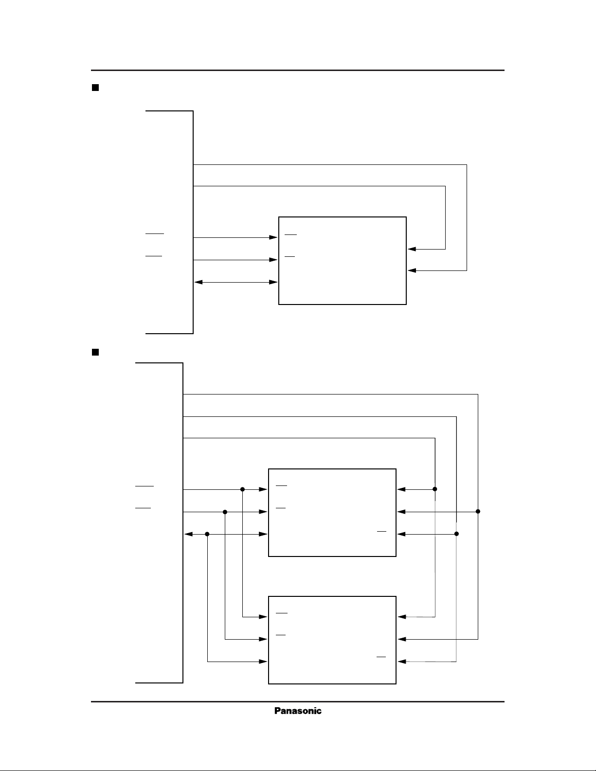
Memory interfaces
• Line lengths up to 2048 pixels 64-Kbit SRAM
× 1
• Line lengths of 2049 to 4096 pixels
64-Kbit SRAM × 2
or 256-Kbit SRAM × 1
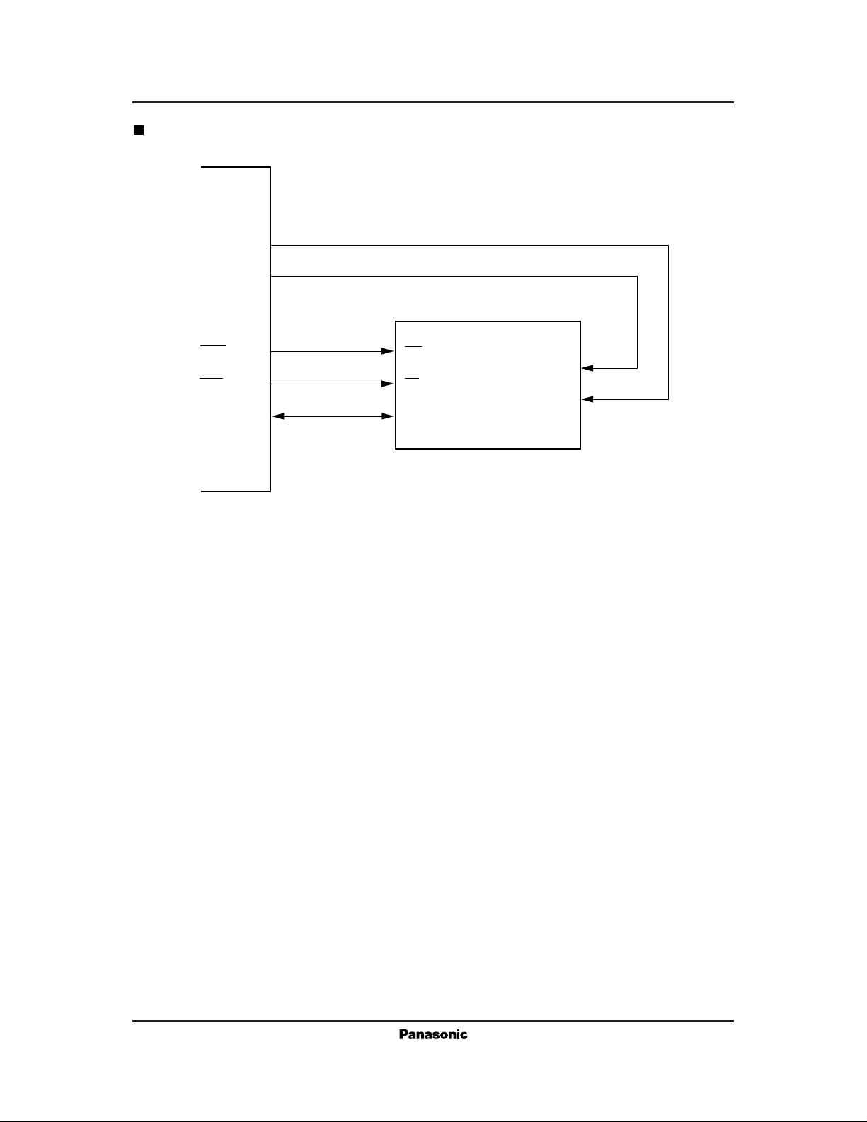
• Line lengths of 4097 to 8192 pixels
256-Kbit SRAM × 1
Image bus interface
• Serial mode with request (VREQ) input and enable
(VSEN), clock (VSCK), and data (VSDA) outputs
Scanning modes
• Free scanning
• Cycle scanning
System interface
• Interface to 8-bit microprocessors (Intel format)
Image data I/O function
• Image data output after shading correction (8 bits)
• Image data output after multivalue smoothing (6 bits)
• Image data input sent from external A/D converter
(8 bits)
Output ports
• 8 pins (pins double as image data I/O pins)
Mechanism drive interface
• User-defined timing pulse output
Power supply
• Digital circuits, DV
• Analog circuits, AV
DD
DD
: 5.0 V
: 5.0 V
• A/D converter reference voltages
: 5.0 to 3.0V
V
REFH
: 2.0 to 0.0V
V
REFL
Applications
Facsimile equipment
Page 3
For Communications Equipment MN86074
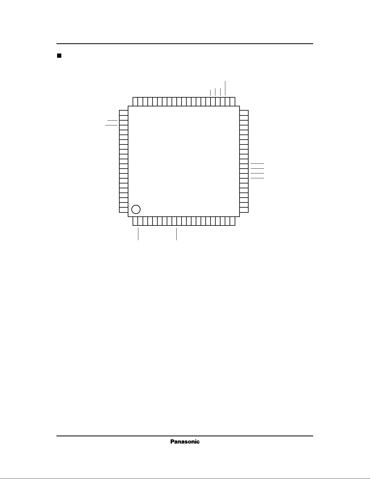
Pin Assigment
SS
MXD2
MXD3
MXD4
MXD5
MXD6
MXD1
MXD0
MOE
MWE
MA14
MA13
MA12
MA11
MA10
MA9
MA8
MA7
MA6
MA5
MA4
MA3
MA2
MA1
MA0
MAST
DV
DD
MXD7D0D1D2D3D4D5D6D7A0A1CSWRRDRESET
636261605958575655545352515049484746454443
64
65
66
67
68
69
70
71
72
73
74
75
76
77
78
79
80
81
82
83
84
123456789
SS
DV
SYNC
FCK2
FCK1
MCLKI
FSH
1011121314151617181920
FR
FSP
PMT
ABC
PEAK
GCDA
CLAMP
VINIG
AGDR
AGUR
AGOUT
FETS
FETG
DV
21
DD
FETD
AV
42
41
40
39
38
37
36
35
34
33
32
31
30
29
28
27
26
25
24
23
22
DV
DD
MOD0
MOD1
VPD0
VPD1
VPD2
VPD3
VPD4
VPD5
VPD6
VPD7
VREQ
VSCK
VSEN
VSDA
OFHC
OFOUT
VREFH
ADIN
VREFL
AV
SS
(TOP VIEW)
QFH084-P-1212
Page 4
MN86074 For Communications Equipment
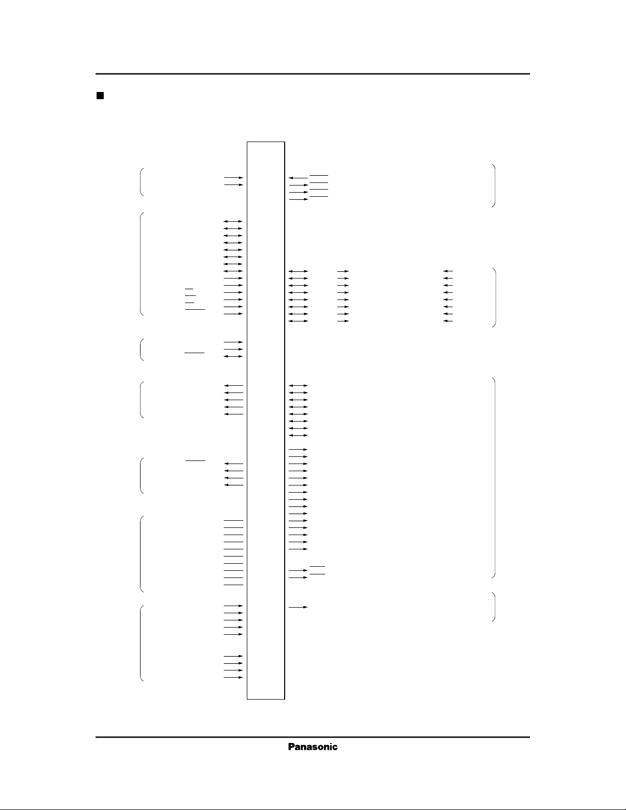
Pin Function Chart
84pin QFP
Mode selection (2)System interface (14)
Clock (3)Sensor interface (5)
Analog pins CNT (4)Analog pins (10)
MOD1
MOD0
D0
D1
D2
D3
D4
D5
D6
D7
A0
A1
CS
WR
RD
RESET
MAST
MCLKI
SYNC
FCK2
FCK1
FR
FSP
FSH
PEAK
CLAMP
ABC
GCDA
OFOUT
OFHC
ADIN
FETS
FETD
FETG
AGOUT
AGUR
AGDR
VINIG
MN86074
VREQ
VSEN
VSCK
VSDA
VPD0
VPD1
VPD2
VPD3
VPD4
VPD5
VPD6
VPD7
MXD0
MXD1
MXD2
MXD3
MXD4
MXD5
MXD6
MXD7
MA0
MA1
MA2
MA3
MA4
MA5
MA6
MA7
MA8
MA9
MA10
MA11
MA12
MA13
MA14
MWE
MOE
SCD0
SCD1
SCD2
SCD3
SCD4
SCD5
SCD6
SCD7
VGSD0
VGSD1
VGSD2
VGSD3
VGSD4
VGSD5
CKVG
PDEL
POD0
POD1
POD2
POD3
POD4
POD5
POD6
POD7
VADD0
VADD1
VADD2
VADD3
VADD4
VADD5
VADD6
VADD7
Image bus interface (5)
Parallel I/O and
output port (8)
Memory interface (25)
Power supply (8)
VREFH
VREFL
AV
DD
AV
SS
DV
DD
DV
DD
DV
SS
DV
SS
PMT
Mechanism drive
interface (1)
Page 5
For Communications Equipment MN86074
Application Circuit Example #1: Line lengths up to 2048 pixels
MN86074
Memory configuration: 64-Kbit SRAM × 1
MA0 to 10
MA13, 14
MWE
MOE
MXD0 to 7
WE
A11, 12
DE
A0 to 10
I/O0 to 7
Application Circuit Example #2: Line lengths of 2049 to 4096 pixels
MN86074
MA0 to 10
MA11
MA13,14
MWE
MOE
Memory configuration: 64-Kbit SRAM × 2
WE
DE
A11, 12
A0 to 10
MXD0 to 7
I/O0 to 7
WE
DE
I/O0 to 7
CS
A11, 12
A0 to 10
CS
Page 6
MN86074 For Communications Equipment
Application Circuit Example #3: Line lengths of 4097 to 8192 pixels
MN86074
Memory configuration: 256-Kbit SRAM × 1
MA0 to 12
MA13, 14
MWE
NOE
MXD0 to 7
WE
A13, 14
DE
A0 to 12
I/O0 to 7
Page 7
For Communications Equipment MN86074
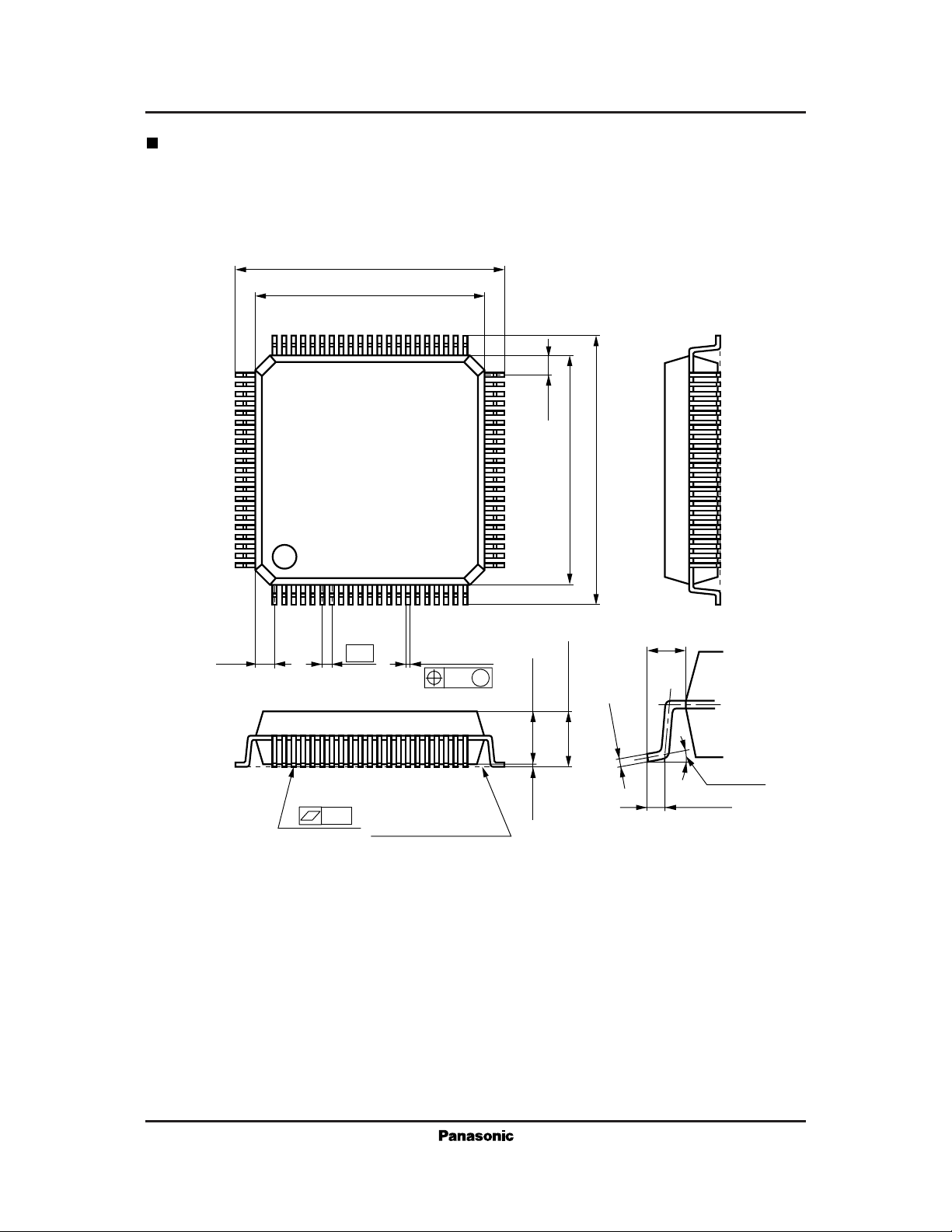
Package Dimensions (Unit: mm)
QFH084-P-1212
14.0±0.2
12.0±0.2
63 43
64
42
84 22
(1.0)
1
0.5
0.2
21
+0.10
–0.05
0.1M
0.1
SEATING PLANE
±0.2
2.8
±0.1
0.1
(1.0)
12.0±0.2
3.2max.
14.0±0.2
+0.10
0.05
-
0.15
(1.0)
0.5
0 to 10°
±0.2
 Loading...