

Page 1
For Video Equipment
MN6761S
External Synchronization Control LSI for Color Video Cameras
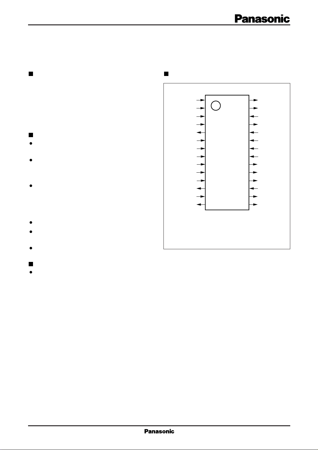
Pin Assignment Overview
The MN6761S is an external synchronization control
LSI for color video cameras.
When used in combination with a synchronizing signal
generator (MN67601NS or MN67602PS), it provides
external synchronization control for NTSC and PAL video
systems.
Features
Synchronization of both the video camera and the
VCR
External synchronization inputs:
Composite synchronizing signal and burst
subcarrier
External synchronization techniques
• Horizontal synchronization: phase-locked loop
• Vertical synchronization: reset technique
• Subcarrier synchronization: phase-locked loop
Support for both NTSC and PAL systems
Built-in feature for automatically switching between
external and internal synchronization
Built-in horizontal phase adjustment circuit
SCPSW1
SCPSW2
WHD
N/P
BGP
GLBSC
V
SS2
V
DD2
GLSYNC
TEST2
f
HPCO
XfHOSCI
XfHOSCO
HP
1
2
3
4
5
6
7
8
9
10
11
12
13
14
(TOP VIEW)
SOP028-P-0375
28
27
26
25
24
23
22
21
20
19
18
17
16
15
4f
4fSCOSCO
4fSCOSCI
SOPCO
SC1
V
V
TEST1
HBLK
EXT/INT
LSWCONT
LSW
VR
Xf
SC
DD1
SS1
H
Applications
Color video cameras
Page 2
MN6761S For Video Equipment
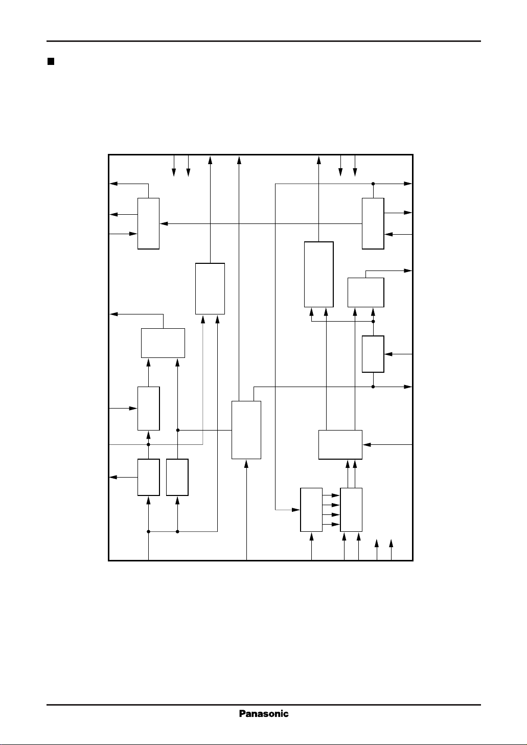
Block Diagram
Xf
Xf
OSCO
Xf
OSCI
HPCO
f
WHD
DD2VSS2
V
8
H
14
H
13
H
oscillator
H
Xf
12
Phase
com-
parator
11
HP
Monostable
multivibrator
7
Internal/external
EXT/INT
19
20
synchronization
switch
HBLK
3
HBLK and BGP
fH
pulse generator
DD1VSS1
V
LSWCONT
18
Line switch control
22
23
pulse generator
Line
Phase
switch
generator
SC
4f
com-
parator
Gate
2815
4f
SC
27
4f
SC
OSCO
26
4f
SC
OSCI
25
SCPCO
6
GLBSC
5
BGP
17
LSW
VR
fV
16
V
separation
H
separation
0˚
90˚
CK
Shift register
Selector
D
10
TEST2
SCPSW2
21
TEST1
9
GLSYNC
1
4
N/P
24
SC1
2
SCPSW1
Page 3
For Video Equipment MN6761S
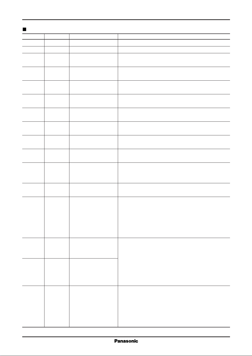
Pin Descriptions
Pin No. Symbol Pin Name Function Description
23 V
22 V
8V
7V
DD1
SS1
DD2
SS2
9 GLSYNC External synchronizing
6 CLBSC External burst
3 WHD Horizontal synchroni-
11 f
HP
24 SC1 Subcarrier input
1 SCPSW1 Subcarrier phase
2 SCPSW2 switch inputs
17 LSW Line switch input
4 N/P NTSC/PAL selection
12 HPCO Horizontal phase
13 XfHOSCI Oscillator input for
14 Xf
15 Xf
OSCO Oscillator output for
H
H
Power supply "H" level (5V) power supply for subcarrier circuits
Power supply "L" level (GND) power supply for subcarrier circuits
Power supply "H" level (5V) power supply for synchronizing signal
circuits
Power supply "L" level (GND) power supply for synchronizing signal
circuits
Input pin for composite synchronizing signal derived from
signal input
video signal (reference for horizontal and vertical signals)
Input pin for burst subcarrier signal derived from video
subcarrier input
signal (reference for subcarrier signals)
Input pin for WHD signal from synchronizing signal
zation input
Monostable multivibrator input
generator
Pin for connecting CR circuit for adjusting delay for analog
monostable multivibrator (thus adjusting horizontal phase)
Input pin for SC1 signal from synchronizing signal
generator
Pin selecting which of the four phase signals generated from
the SC1 signal goes to the phase comparator
For a PAL system, supply the LSW signal from the
synchronizing signal generator.
For an NTSC system, keep this pin at "H" level.
"H" level selects NTSC operation;
input
"L" level, PAL operation.
This pin is at "L" level when the WHD signal, after passing
comparator output
through the monostable multivibrator, leads the rising edge
of the HSYNC signal derived by separating off the
horizontal component of the GLSYNC signal and is at "H"
level when the signal lags. At all other times, it is in the
high-impedance state.
Clock oscillator pins for the synchronization circuits.
the synchronization
circuits
Connect these pins to an inductor, capacitor, and variable
capacitor. (The pins have built-in feedback resistors.)
The circuit oscillates during external synchronization mode.
the synchronization
circuits
Clock output for
synchronizing signal
circuits
The oscillation stops for internal synchronization mode.
The oscillator frequency, Xf
NTSC and 4.406 MHz (282f
is 14.31818 MHz (910fH) for
H
) for PAL.
H
Clock output pin for synchronizing signal circuits.
This pin provides the clock (Xf
) for the external
H
synchronization mode and stays at "L" level for the internal
synchronization mode. Connect to the EX910f
I pin of the
H
synchronizing signal generator for NTSC operation and to
the EX282f
I pin for PAL operation.
H
Page 4
MN6761S For Video Equipment
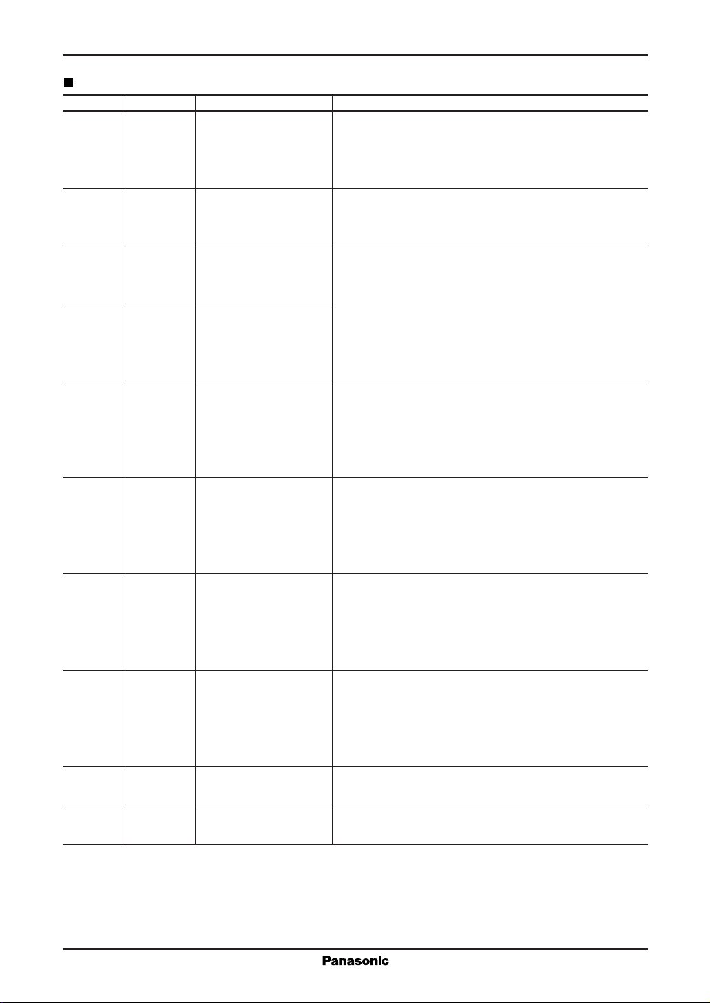
Pin Descriptions (continued)
Pin No. Symbol Pin Name Function Description
16 VR Vertical reset output
25 SCPCO Subcarrier phase
comparator output
26 4fSCOSCI Oscillator input for
subcarrier circuits
27 4fSCOSCO Oscillator output for
subcarrier circuits
28 4f
SC
Subcarrier clock output
18 LSWCONT Line switch polarity
control output
19 EXT/INT Automatic internal/
external switching
output
5 BGP Burst gate pulse output
20 HBLK Horizontal blanking
output
21 TEST1 Test inputs
10 TEST2
This pin generates a vertical reset pulse for the
V-SERATION interval detected in the GLSYNC signal.
Connect it to the VR pin of the synchronizing signal
generator.
This pin is at "L" level when the SC1 signal leads the
GLBSC signal and is at "H" level when the signal lags.
At all other times, it is in the high-impedance state.
Clock oscillator pins for the subcarrier circuits.
Connect these pins to a crystal oscillator, capacitor, and
variable capacitor. (The pins have built-in feedback resistors.)
The circuit oscillates during external synchronization mode.
The oscillation stops for internal synchronization mode.
The oscillator frequency, 4f
is 14.31818 MHz for NTSC
SC ,
and 14.734 MHz for PAL.
Clock output from subcarrier circuits.
In external synchronization mode, this pin provides the
) clock signal; in internal synchronization mode, it
(4f
SC
remains at "L" level. Connect this pin to the EX4f
I pin on
SC
the synchronizing signal generator.
During PAL operation, this pin emits an error detection
pulse if the LSW polarity is wrong, and the chip reverses
the LSW polarity. During internal synchronization mode,
this pin remains at "L" level. Connect this pin to the
LSWCONT pin on the synchronizing signal generator.
If the chip detects GLSYNC input, it switches to external
synchronization mode and drives this pin at "H" level.
Otherwise, it switches to internal synchronization mode and
drives this pin at "L" level. Connect this pin to the EXT/INT
pin on the synchronizing signal generator.
These pulses have a width of 2.5 µs (NTSC) or 2.3 µs
(PAL) and trail the rising edge of the HSYNC signal by
5.3 µs (NTSC) or 5.6 µs.
They are generated for only 10 H to 256 H (NTSC) or
304 H (PAL) after the VR pulse.
These pulses have a width of 8.9 µs (NTSC) or 8.8 µs
(PAL) and follow the rising edge of the HSYNC signal.
Leave these test inputs open. (The pins include built-in
pull-up resistors.)
Page 5
For Video Equipment MN6761S
Timing Chart
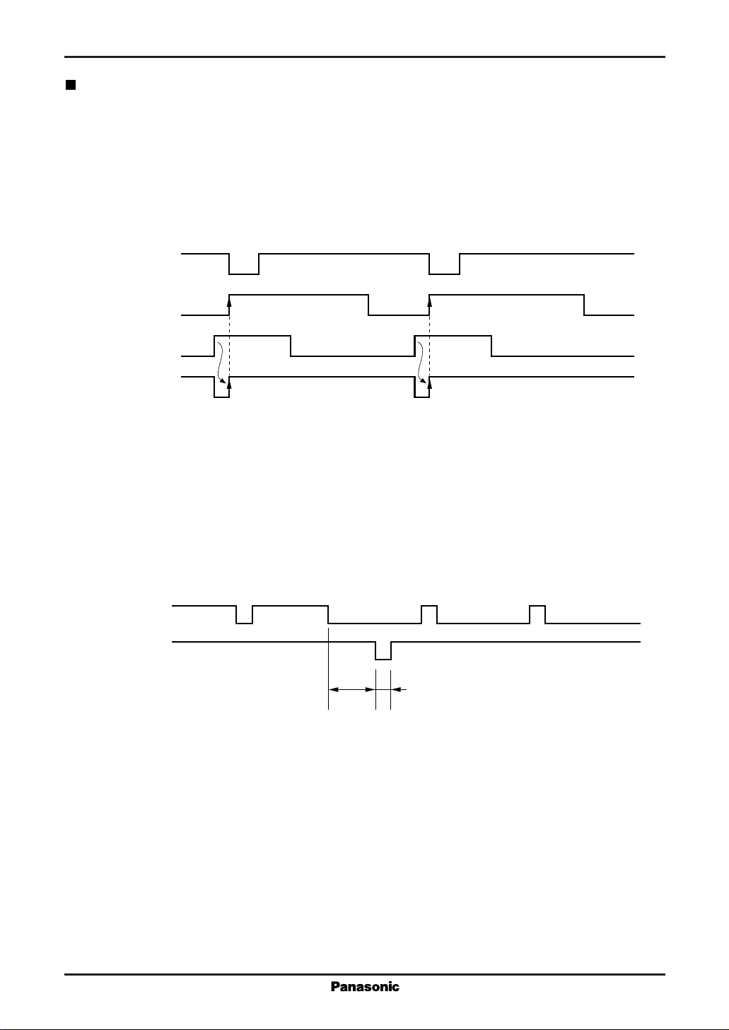
1. Horizontal synchronization block
This block compares the phases of the HSYNC signal derived by separating off the horizontal component of
the GLSYNC input and the WHD signal from the synchronizing signal generator after it has passed through
the monostable multivibrator. It is thus possible to adjust the horizontal phase by adjusting the CR integral
circuit's time constant.
GLSYNC
HSYNC
WHD
DELAY
WHD
Timing chart for horizontal pulse phase comparison
2. Vertical synchronization block
This block detects the V-SERATION interval in the GLSYNC input and generates a vertical reset (VR) pulse
with 0.5 H of the start of that interval. It then issues no pulses for 256 H (NTSC) or 304 H (PAL) after this
VR pulse.
GLSYNC
VR
2.2µs (NTSC
1.8µs (PAL
14.0µs (NTSC
11.2µs (PAL
Vertical reset pulse timing chart
)
)
)
)
Page 6
MN6761S For Video Equipment
3. Subcarrier synchronization block
This block converts the SC1 output from the synchronizing signal generator into four signals with the same
frequency as the burst subcarrier, but different phases. In this phase-locked loop circuit, the phase of GLBSC
is compared with the phase selected by 2 bits (SCPSW1 and SCPSW2).
During PAL operation, if the LSW polarity is wrong, this block sends an error detection pulse (LSWCONT)
to the synchronizing signal generator and reverses the LSW polarity. It also adjusts the relationship between
fields 1 through 4.
4. Oscillator blocks
The XfH and 4fSC oscillator blocks operate only during external synchronization mode. Connecting a variable
capacitor creates voltage-controlled oscillators that generate the synchronization signal circuit clock (Xf
and subcarrier circuit clock (4f
) for output to the synchronization signal generator.
SC
5. Automatic internal/external switching block
If it detects a minimum of ten edges from the GLSYNC input, this block switches the chip to the external
synchronization mode and drives the EXT/INT pin at "H" level. If there are no edges in the GLSYNC input
for 10 H, this block switches the chip to the internal synchronization mode and drives this pin at "L" level.
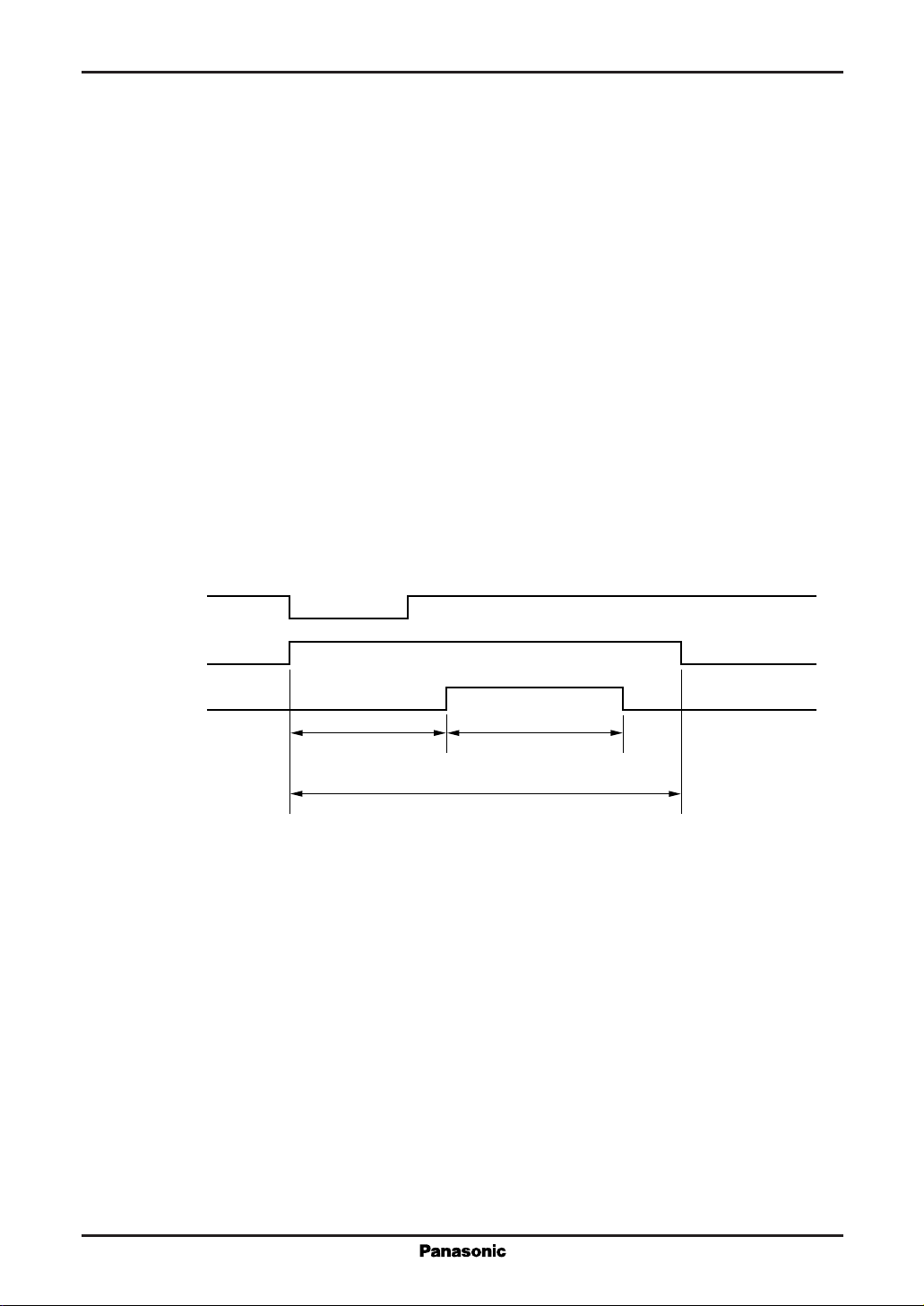
HBLK and BGP plus generator
)
H
GLSYNC
HBLK
BGP
5.3µs (NTSC
5.6µs (PAL
There is an HBLK pulse for each H.
BGP pulses are generated for only 10 H to 256 H (NTSC) or 304 H (PAL) after the VR pulse.
)
)
8.9µs (NTSC
8.8µs (PAL
HBLK and BGP pulse timing chart
2.5µs (NTSC
2.3µs (PAL
)
)
)
)
Page 7
For Video Equipment MN6761S
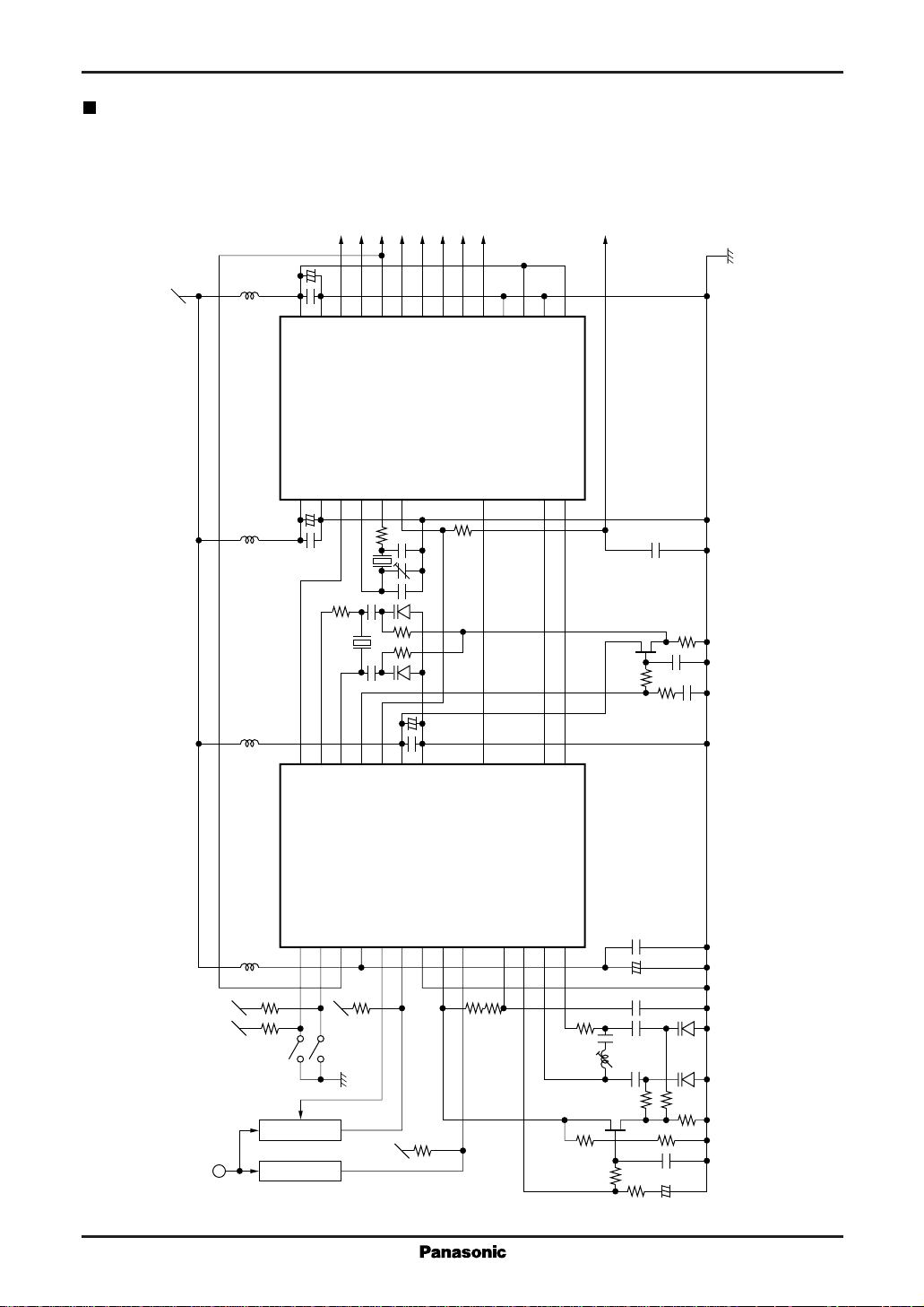
Application Circuit Example
1. External synchronization for NTSC system
SC1
+
2.2µH
2.2µH
2.2µH
2.2µH
10µF
10000pF
25
26
27
28
V
V
DD2
DD1
SS2
V
SS1
V
VP VP
SYNC SYNC
I
SC
OSCI
EX4f
4f
SC
24WHD WHD
OSCO
SC
4f
1234567891011
+
10µF
18pF
1kΩ
X2
330pF
X1
330pF
1kΩ
100kΩ
100kΩ
10000pF
+
24
25
26
27
28
SC
4f
OSCO
SC
4f
SCPSW2
SCPSW1
OSCI
SC
4f
WHD
SC1
SCPCO
BGP
N/P
1234567891011
100kΩ
100kΩ
100kΩ
22212019181716
23
BF BF
BLK BLK
SC1
10pF
CP2 CP2
CP1V CP1V
SC2
BSC
20pF
1kΩ
WBLK WBLK
VPCO
EXT/INT
SW1
CP1
D4
D3
10µF
10000pF
23
22212019181716
SS1
DD1
V
V
GLBSC
SS2
V
HBLK
TEST1
DD2
V
GLSYNC
10kΩ
EXT/INTTEST2
LSWCONT
f
50kΩ
SW2
TEST
121314
LSW
HP
HPCO
121314
15
SW4
SW3
I
H
VR
EX910f
15
H
VRXf
OSCI
OSCO Xf
H
H
Xf
1kΩ
10000pF
MN67601NS
180pF
3kΩ
100pF
22Ω
220kΩ
MN6761S
10000pF
+
10µF
47pF
330pF
330pF
39000pF
D2
D1
14.31818MHz
X1,2
D1 to 4 1SV153
2SK198
5V
VBS
Burst Sep.
Sync Sep.
100kΩ
100kΩ
1kΩ
10kΩ
100kΩ
1000pF
43kΩ
10kΩ
3kΩ
2SK128
2.2µF
+
Page 8
MN6761S For Video Equipment
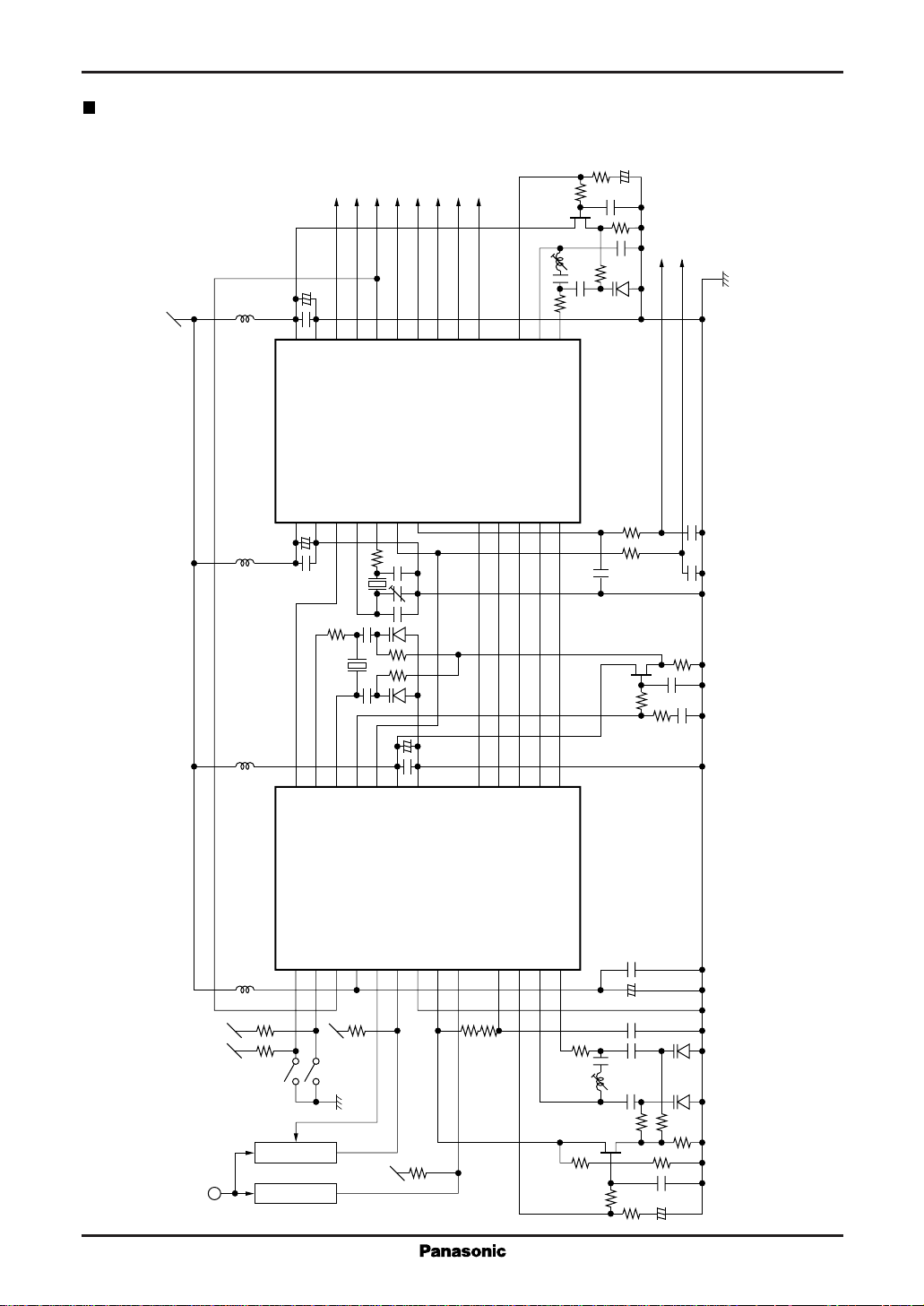
Application Circuit Example
2. External synchronization for PAL system
7.5kΩ
2.2µF
1200pF
1kΩ
3kΩ
Q3
SC1
SC2
D5
MN67602PS
1kΩ
180pF
1kΩ
180pF
2SK198
Q1 to 3
D1 to 5 1SV153
17.734MHz
X1,2
5V
2.2µH
2.2µH
+
10µF
10000pF
24WHD WHD
25
26
27
28
SS2
V
SS1
V
VP VP
SYNC SYNC
I
SC
OSCI
SC
EX4f
4f
OSCO
SC
4f
V
V
DD2
DD1
1234567891011
+
10µF
18pF
10000pF
1kΩ
X2
23
22212019181716
BF BF
CP2 CP2
BLK BLK
CP1V CP1V
WBLK WBLK
SC1
SC2
BSC
VPCO
EXT/INT
20pF
1000pF
1kΩ
OSCI
HPCO
H
SCBLK
282f
LSWCONT
LSW
VR
121314
330pF
15
OSCO
H
I 282f
H
EX282f
15pF
10kΩ
12pF
VBS
2.2µH
2.2µH
330pF
1kΩ
100kΩ
100kΩ
X1
330pF
+
24
25
26
27
28
SC
4f
OSCO
SC
4f
SCPSW2
SCPSW1
OSCI
SCPCO
SC
4f
WHD
N/P
SC1
BGP
1234567891011
100kΩ
100kΩ
Burst Sep.
100kΩ
100kΩ
Sync Sep.
10pF
D4
D3
10µF
10000pF
23
22212019181716
SS1
DD1
V
V
GLBSC
SS2
V
HBLK
TEST1
DD2
V
GLSYNC
10kΩ
EXT/INTTEST2
50kΩ
VRXf
LSW
LSWCONT
OSCI
H
HP
f
HPCO
121314
10000pF
15
H
OSCO Xf
H
Xf
1kΩ
100kΩ
Q2
MN6761S
10000pF
+
330pF
330pF
Q1
100kΩ
1000pF
43kΩ
1kΩ
22Ω
220kΩ
10µF
47pF
10kΩ
3kΩ
100pF
39000pF
D2
D1
10kΩ
3kΩ
2.2µF
+
Page 9
For Video Equipment MN6761S
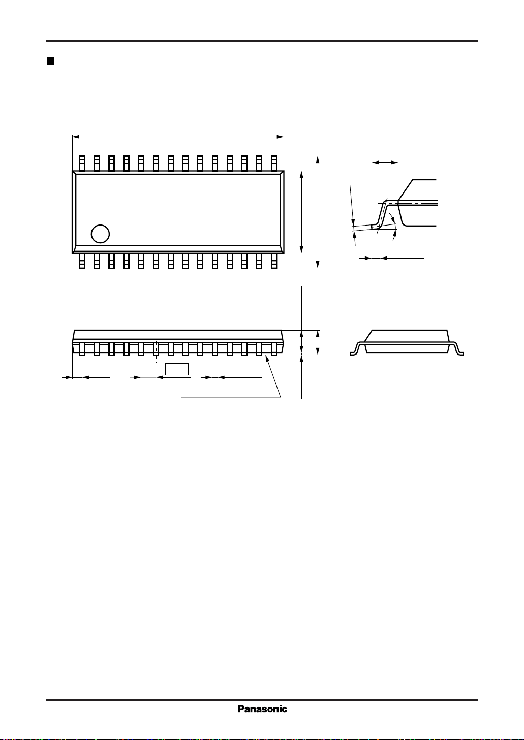
Package Dimensions (Unit: mm)
SOP028-P-0375
17.80
±0.20
28
15
0.05
-
+0.10
1.10±0.20
0.15
7.20±0.202.00±0.200.10±0.10
0 to 10°
0.30min.
114
2.40max. 9.40±0.30
(0.65) 0.40
1.27
±0.10
SEATING PLANE
 Loading...