

Page 1
For Information Equipment
MN89201
VGA-NTSC Scan Converter
Overview
The MN89201 converts PC/AT VGA (640 × 480) display
data into an NTSC video signal without requiring an external
frame memory. It uses filtering to eliminate flicker and
produce a high-quality television image.
Note: PC/AT and VGA are registered trademarks of International
Business Machines Corporation.
Features
Conversion of PC/AT VGA (640 × 480) display data
into NTSC video signal
• 8-bit inputs for VGA R, G, and B signals
Horizontal frequency: 31.5 kHz
Vertical frequency: 59.94 Hz
• Conversion of non-interlaced display to interlaced
display
• Built-in phase-locked loop for synchronizing VGA
and NTSC data clocks
• Conversion from RGB to YCrCb (4:2:2) format
• Data output in NTSC display format (YCrCb24 or
YCrCb16-bit)
Flicker prevention
• Choice of line filters with 3 taps for preventing
flicker
Processing with only line memory
• No need for external VRAM
• All processing completes within built-in line memory
Choice of readout clocks for NTSC output
Choice 1: Choice of clock that has arbitrary
frequency and synchronizes with
VGA clock
External voltage-controlled
oscillator in addition to built-in
phase-locked loop
Choice 2: Choice of clock that has arbitrary
frequency and does not synchronize
with VGA clock
External oscillator
Choice 3: Clock with half frequency of the
VGA-dot-clock
Choose the clock matching the NTSC encoder.
The MN89201 offers high-quality NTSC-compatible
output from a compact configuration.
Applications
Point-of-sale terminals, Factory automation terminals,
word processors, and other terminals
Page 2
MN89201 For Information Equipment
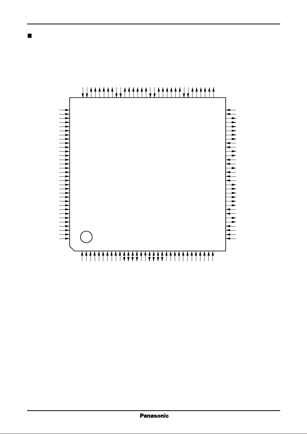
Pin Assignment
SSVDD
YOUT7
YOUT6
YOUT5
YOUT4
YOUT3
YOUT2
VSSVDDYOUT1
YOUT0
CROUT7
CROUT6
CROUT5
CROUT4
VSSVDDCROUT3
CROUT2
CROUT1
CROUT0
CBOUT7
CBOUT6
VSSVDDCBOUT5
CBOUT4
CBOUT3
CBOUT2
CBOUT1
V
CBOUT0
TEST0
TEST1
TEST2
TEST3
TEST4
BIN0
BIN1
BIN2
BIN3
BIN4
BIN5
BIN6
BIN7
GIN0
GIN1
GIN2
GIN3
GIN4
GIN5
GIN6
GIN7
RIN0
RIN1
RIN2
RIN3
RIN4
RIN5
RIN6
RIN7
XVSYNCIN
XHSYNCIN
DOTCLK
96959493929190898887868584838281807978777675747372717069686766
97
98
99
100
101
102
103
104
105
106
107
108
109
110
111
112
113
114
115
116
117
118
119
120
121
122
123
124
125
126
127
128
12345678910111213141516171819202122232425262728293031
SS
DD
V
V
AEN
XRD
XWE
RA3
RA2
RA1
RA0
REGLIN
DB7
DB6
DB5
DB4
SS
DD
V
V
DB3
DB2
DB1
DB0
SS
DD
V
V
RESET
MODSET1
MODSET0
MODPIN
MOD422F
MODVFIL
MODHFIL
65
64
63
62
61
60
59
58
57
56
55
54
53
52
51
50
49
48
47
46
45
44
43
42
41
40
39
38
37
36
35
34
33
32
MON1
MON0
MINTEST
V
DD
V
SS
RDCLK
XENCRST
XBLANK
XVSYNC
XHSYNC
RD2CLK
V
DD
V
SS
OEON
OEOP
V
DD
V
SS
XOO
OSXIN
V
DD
V
SS
MEMOUT0
MEMOUT1
MEMOUT2
MEMOUT3
MEMOUT4
MEMOUT5
V
DD
V
SS
MEMOUT6
MEMOUT7
MODST
MODCHAV
MODCRCB
SXRST
Note: Never leave V
QFH128-P-1818
and VSS pins open.
DD
(TOP VIEW)
Page 3
For Information Equipment MN89201
Block Diagram
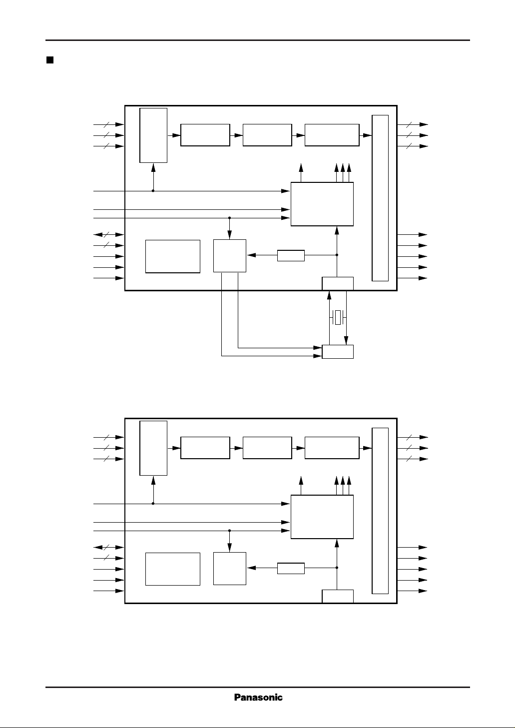
• RDCLK from an external VCO clock synchronized with VGA clock
8
R
8
G
8
B
DOTCLK
XVSYNCIN
XHSYNCIN
DB[7:0]
RA[3:0]
8
4
CS (AEN)
WR
RD
• RDCLK from VGA clock
Latch
RGB-YCrCb
converter
Flicker
elimination
block
Registers PLL 1/N
OEOP
Conversion from
non-interlaced to
interlaced display
Control block
counters,
pulse generator, etc.
lead
lag
OSC I/F
VCO
8
Y
8
Cr
8
Cb
Coding interface
XVSYNC
XHSYNC
BLANK
RD2CLK
RDCLK
XOOOSXINOEON
DOTCLK
XVSYNCIN
XHSYNCIN
DB[7:0]
RA[3:0]
CS (AEN)
WR
RD
8
R
8
G
8
B
Latch
RGB-YCrCb
converter
Flicker
elimination
block
Conversion from
non-interlaced to
interlaced display
Control block
counters,
pulse generator, etc.
8
Y
8
Cr
8
Cb
Coding interface
8
4
Registers PLL 1/N
XVSYNC
XHSYNC
BLANK
RD2CLK
OSC I/F
RDCLK
Page 4
MN89201 For Information Equipment
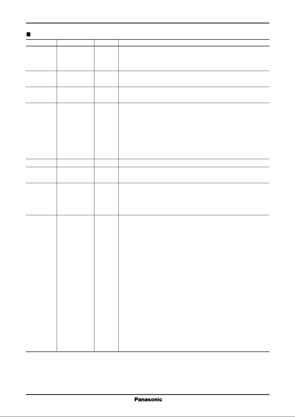
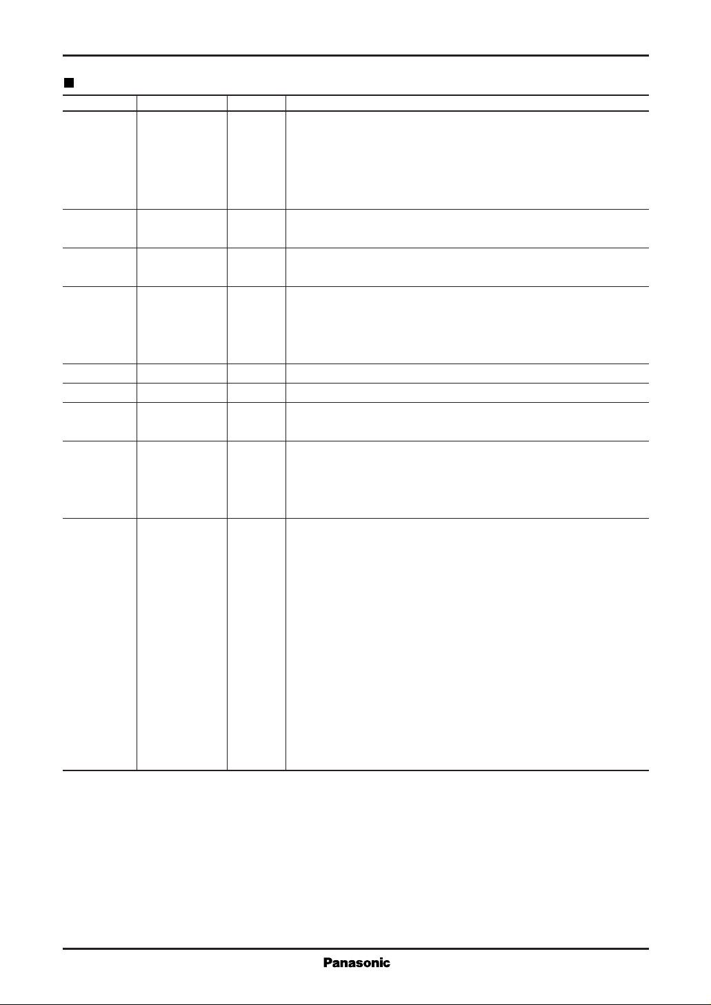
Pin Descriptions
Pin No. Symbol I/O Function Description
3 AEN I Chip select signal
"L" level: Register access enabled
"H" level: Register access disabled
4 XRD I Read control signal
"L" level: Read enabled
5 XWE I Write control signal
"L" level: Write enabled
6 REGLIN I Register address mode specification
"H" level: Obtain register address from RA[3:0]
"L" level: Obtain register address from address register
In the latter case, the address of the parameter/mode register are
specified by the address register .
Address register: 0H (4-bit decode)
Data register: 1H (4-bit decode)
7 to 10 RA[3:0] I Register address specification
11 to 14 DB[7:0] I Host data bus
17 to 20
23 RESET I MN89201 reset signal
Active "H"
This signal initializes internal registers to their default values and
resets internal synchronization counters.
24 ,25 MODSET[1:0] I Synchronization mode specification pins
These specify the RDCLK synchronization mode for output signals
to the NTSC encoder
(1:0)
0 0: Use an external VCO clock signal synchronized with the VGA
clock signal for RDCLK. The XH, XVSYNC, XBLANK, and
XENRST signals are generated inside the MN89201 and are
outputted. (synchronous)
0 1: Use an external oscillator clock signal not synchronized with
the VGA clock signal for RDCLK. The XH and XVSYNC
signals are retimed versions of the VGA H and VSYNC
signals. (asynchronous)
The other outputs use the VGA DOTCLK signal.
1 0: Use the VGA DOTCLK signal for RDCLK. The YCrCb data,
XVSYNC, XBLANK, and XENRST signals all are dealt in
the VGA clock. An external oscillator is not necessary.
(synchronous)
Page 5
For Information Equipment MN89201
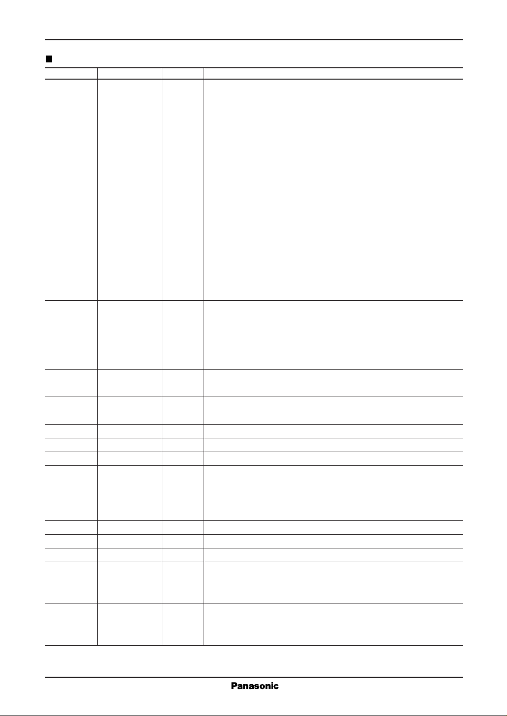
Pin Descriptions (continued)
Pin No. Symbol I/O Function Description
26 MOD422F I Cr and Cb output mode specification
"L" level: Cr and Cb are both 8 bits (24-bit mode)
"H" level: Cr and Cb are multiplexed into 8 bits (16-bit mode)
The combined output is sent to CROUT[7:0].
The MODCRCB pin specifies the multiplex order.
27 MODVFIL I This pin switches the vertical filter ON and OFF.
"L" level: OFF; "H" level: ON
28 MODHFIL I This pin switches the horizontal filter ON and OFF.
"L" level: OFF; "H" level: ON
29 MODPIN I This pin selects the setting of the filter mode.
"H" level: Ignore mode register setting and take filter settings from
pins.
"L" level: Ignore pins and take filter settings from mode register.
30 MINTEST I Test pin Keep this pin at "L" level.
31 ,32 MON[1:0] I Test pin Keep this pin at "L" level.
33 SXRST I This signal resets the synchronization counter only.
Active "H"
34 MODCRCB I This pin specifies the bit order for multiplexed Cr and Cb output data
in the 16-bit mode.
"H" level: Cr before Cb
"L" level: Cb before Cr
35 MODCHAV I This pin selects the default values for the parameter registers
determining the vertical position of the television image.
"H" level: Use the default setting that centers the PC image in the
television display.
Setting value is 45 for back porch and 530 for active end.
These settings cause one or two PC lines to be lost at both
the top and bottom.
"L" level: Use the default settings that align the center of the PC
image at two or three lines below the center of the
television display.
Setting value is 35 for back porch and 514 for active end.
These settings doesn’t lose the tops of the images but
cause three or four lines to be lost at the bottom.
Page 6
MN89201 For Information Equipment
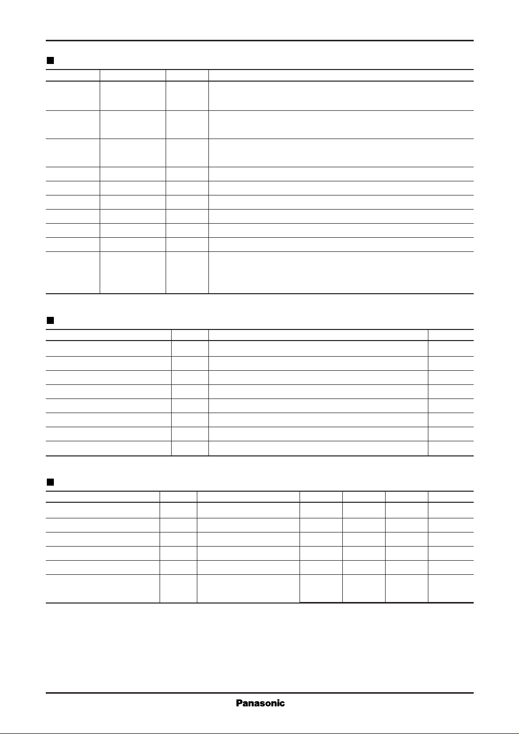
Pin Descriptions (continued)
Pin No. Symbol I/O Function Description
36 MODST I This pin selects the output signal to the monitor pin, MEMOUT7
(pin 37).
"H" level: Pin 37 (normally "H" level) indicates the phase informa-
tion of VSYNC signal in VGA when the MN89201 is in
synchronization.
Note: At the time when RESET (pin 23) or SXRST
(pin 33) is driven (turned-ON or -OFF), the inner
counter of the MN89201 begins to operate in phase
with H and VSYNC of VGA. So, the phase shift in
VGA after synchronization can cause wrong
display. In this case you should survey the phase
information in synchronization that is outputted
from this pin, and detect the phase variation of the
synchronous signal in VGA, then give RESET or
SXRST to the MN89201.
"L" level: Test signal output.
37 MEMOUT7/ O If the MODST pin (pin 36) is "H" level, this pin indicates phase
SYNCINF information in synchronization of internal counters and VGA
synchronizing signals.
If pin 36 is "L" level, this pin is output for a test. Should be left open
usually.
38 MEMOUT O Test pin
41 to 46 [6:0] Normally leave this pin open.
49 OSXIN I External oscillator input pin
If an external oscillator is not used, drive this pin at "L" level.
50 XOO O External oscillator output pin
53 OEOP O Internal PLL comparator result signal
54 OEON O Internal PLL comparator result signal
57 RD2CLK O This data clock is half the frequency of RDCLK, has the same
frequency as the clock for Y, Cr, and Cb outputs.
The XHSYNC, XVSYNC, and XBLANK signals have a retiming at
the rising edge of this clock signal.
58 XHSYNC O Horizontal synchronizing output signal (Active "L")
59 XVSYNC O Vertical synchronizing output signal (Active "L")
60 XBLANK O Composite blanking output signal (Active "L")
61 XENRST O Encoder reset signal (Active "L")
This signal has four fields interval (when both H and V are at "L"
level.) Use it as necessary to control the NTSC encoder.
62 RDCLK O Encoder clock
Y, Cr, and Cb outputs to the NTSC encoder are synchronized with
the rising edge of this clock signal.
Page 7
For Information Equipment MN89201
Pin Descriptions (continued)
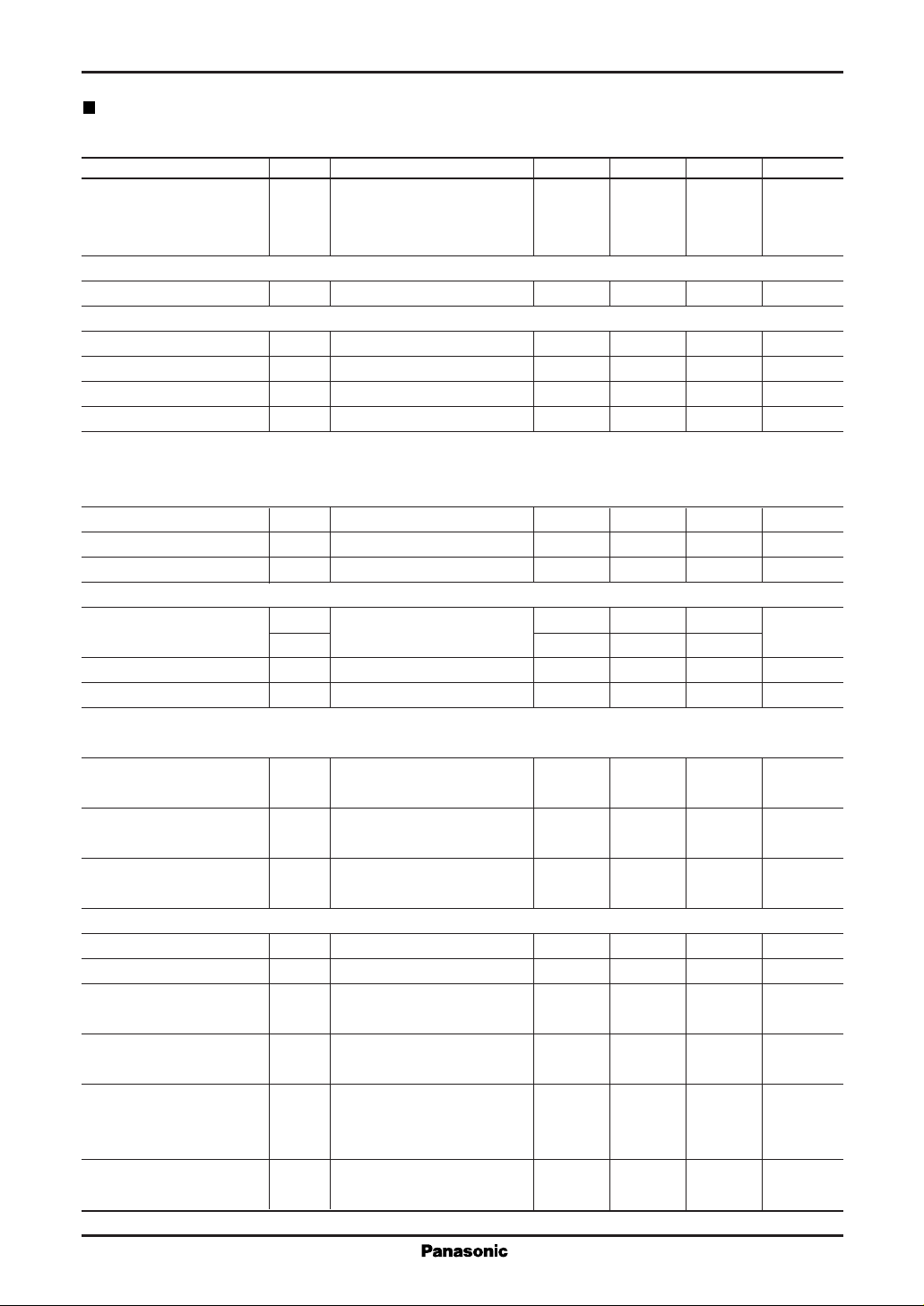
Pin No. Symbol I/O Function Description
65 to 70 CB OUT[7:0] O In the 24-bit mode, color difference output (CB: B-Y). And in the
73 to 74 16-bit mode, CBOUT0 gives the Cr flag: "H" level for Cr output.
75 to 78 CR OUT[7:0] O In the 24-bit mode, color difference output (CR: R-Y). And in the
81 to 84 16-bit mode, these pins yield multiplexed Cr/Cb output.
85 to 86 Y OUT[7:0] O Luminance signal output (Y)
89 to 94
97 to 101 TEST[4:0] I Test pins Keep these pins at "L" level.
102 to 109 BIN[7:0] I Blue input signals
110 to 117 GIN[7:0] I Green input signals
118 to 125 RIN[7:0] I Red input signals
126 XVSYNCIN I VVGA horizontal synchronizing input signal (Active "L")
127 XHSYNCIN I VGA vertical synchronizing input signal (Active "L")
128 DOTCLK I VGA dot clock
The chip latches input data from VGA at the rising edge of this clock
signal.
Absolute Maximum Ratings
Parameter Symbol Ratings Unit
Power supply voltage V
Input pin voltage V
Output pin voltage V
Output current I
Output current I
Power dissipation P
Operating ambient temperature T
Storage temperature T
DD
I
O
OL
OH
D
opr
stg
– 0.3 to +7.0 V
– 0.3 to VDD+0.3 V
– 0.3 to VDD+0.3 V
+12 mA
– 12 mA
1000 mW
– 40 to +70 ˚C
– 55 to +150 ˚C
Recommended Operating Conditions
Parameter Symbol Conditions min typ max Unit
Power supply voltage V
DD
Ambient temperature Ta 0 70 ˚C
Rise time for input t
Fall time for input t
Oscillation frequency f
Recommended value C
for external capacitance C
r
f
Crystal oscillator 24 MHz 24 MHz
osc
VDD=5.0V 12 pF
XI
Built-in feedback resistor 12 pF
XO
4.75 5.0 5.25 V
0 150 ns
0 150 ns
Page 8
MN89201 For Information Equipment
Electrical Characteristics
VDD=4.75 to 5.25V, VSS=0.00V, f=25MHz, Ta=0 to 70˚C
Parameter Symbol Conditions min typ max Unit
Power supply current I
DD
VI=VDD or V
SS
during operation f=25MHz
VDD=5.0V Output open
Oscillator circuit XOO
Built-in feedback resistance R
fb
VI=VDD or V
=5.0V 228 570 1430 k Ω
SS, VDD
CMOS level input with pull-down resistor: MINTEST
"H" level input voltage V
"L" level input voltage V
Pull-down resistance R
Input leakage current I
IH2
IL2
PD1VI=VDD, VDD
LIPDVI=VSS
=5.0V 12 30 75 kΩ
V
× 0.7 V
DD
0V
TTL level inputs: RA0 to 3, AEN, BIN0 to 7, GIN0 to 7, MOD422F, RIN0 to 7, XRD, XWE, TEST0 to 4,
MODST, DOTCLK, MODPIN, MODSET0 to 1, REGLIN, MODCHAV, MODCRCB, MODHFIL, MODVFIL,
XHSYNCIN, XVSYNCIN
"H" level input voltage V
"L" level input voltage V
Input leakage current I
IH1
IL1
LI
VI=VDD or V
SS
2.0 V
0 0.8 V
TTL level inputs with Schmidt input: SRST, RESET
Input threshold voltage V
tHLVDD
V
tLH
=4.75 to 5.25V 1.8 2.4 V
0.4 1.0
Hysteresis width ∆VttVDD=5.0V 0.4 0.8 V
Input leakage current I
LI
VI=VDD or V
SS
Push-pull outputs: RD2CLK, OEON, OEOP, YOUT0 to 7, CBOUT0 to 7, CROUT0 to 7, RDCLK,
MEMOUT0 to 7, XBLANK, XHSYNC, XVSYNC, XENRST
"H" level output voltage V
"L" level output voltage V
Peak output current I
O (Peak)
OHIO
=–4 .0mA VDD– 0.6 V
VI=V
OLIO
VI=V
or V
DD
SS
=4.0mA 0.4 V
or V
DD
SS
Absolute maximum rating – 12 12 mA
(not guaranteed operating value)
CMOS level I/O: DB0 to DB7
"H" level input voltage V
"L" level input voltage V
"H" level output voltage V
"L" level output voltage V
Output leakage current I
Peak output current I
O (Peak)
IH2
IL2
OHIO
LO
=–4.0mA VDD–0.6 V
VI=V
OLIO
VI=V
or V
DD
SS
=4.0mA 0.4 V
or V
DD
SS
VO=High-impedance state ±10 µA
I=VDD
DD
or V
or V
SS
SS
V
VO=V
Absolute maximum rating –12 12 mA
(not guaranteed operating value)
V
× 0.7 V
DD
0V
126 mA
DD
× 0.3 V
DD
±20 µA
DD
±10 µA
±10 µA
DD
× 0.3 V
DD
V
V
V
Page 9
For Information Equipment MN89201
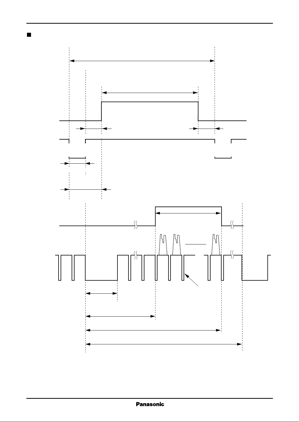
Timing Chart
780
clock cycles
640
clock cycles
Active interval
(horizontal)
Horizontal
synchronization
Active interval
(vertical)
Vertical
synchronization
clock cycles
Horizontal
synchronizing
signal
58
clock cycles
118
clock cycles
Back
porch
60
Vertical
synchronizing
signal
480 lines
Front
porch
22
clock cycles
Horizontal
synchronizing
signal
Vertical
synchronizing
signal
2 lines
35 lines
(for a readout frequency of 12.27 MHz)
515 lines
525 lines
Horizontal
synchronizing
signal
Page 10
MN89201 For Information Equipment
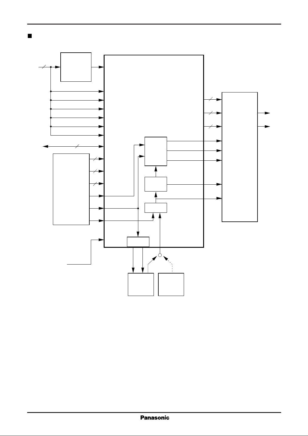
Application Circuit Example
SA
DB
16
Address
decoder
8
VGA
8
8
8
25.175MHz
(VGACLK)
AEN
RA0
RA1
RA2
RA3
XRD
XWE
RIN
GIN
BIN
XVSYNCIN
XHSYNCIN
DOTCLK
MN89201
PLL
Counters
1/2nd
frequency
divider
SEL
YOUT
CROUT
CBOUT
XHSYNC
XVSYNC
XENRST
RD2CLK
RDCLK
8
8
8
NTSC
encoder
Y
C
RESET
VCO1 OSC
Notes: Choose the clock frequencies to match the synchronization system for the NTSC encoder. The PLL
uses the VGA XHSYNCIN (31.5 MHz) clock signal for comparison.
The XHSYNC, XVSYNC, and XENRST signals to the NTSC encoder are synchronized with the
VGA outputs.
Page 11
For Information Equipment MN89201
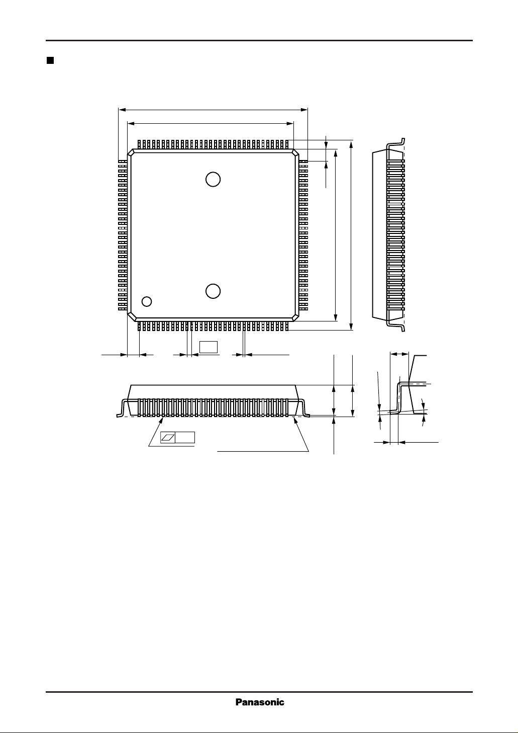
Package Dimensions (Unit: mm)
QFH128-P-1818
20.0±0.2
18.0
±0.2
96 65
97
(1.25)
64
(1.25)
18.0±0.2
20.0±0.2
33128
132
–0.05
+0.10
1.0±0.2
0.5
0.2±0.1
3.3±0.2
3.4±0.3
0.15
0.1
SEATING PLANE
0.1±0.1
0.5±0.2
0 to 10°
 Loading...