

Page 1
For Communications Equipment
MN86063
High-Speed CODEC LSI for Facsimile Images
Overview
The MN86063 is a high-speed LSI codec for compressing
and decompressing facsimile images. Features include
real-time printing to laser printers, built-in line memory,
enlargement and reduction, and code conversion.
Features
Pixels per line:
between 16 and 4864 bits, in word (16-bit) increments.
Processing time per line:
Individual pixels are processed within two system
clock cycles. For a machine cycle of 10 MHz,
processing the worst-case pattern for a 4096-bit line
takes no more than 1 ms.
Time-shared, multiplex processing
Support for time-shared, multiplex processing allows
image I/O, enlargement/reduction processing, and
coding/decoding to proceed concurrently for a group
of lines. Image bus DMA transfers can also proceed
concurrently with command processing.
Multiple channels
If lines consist of 2432 bits or fewer, commands can
be processed simultaneously on two channels using
time-sharing. These commands may be issued
asynchronously.
Bus configuration
There are separate system and image buses. The latter
features two independent master DMA channels; the
former, four slave DMA channel pins.
Image data I/O
Image data I/O can use either the image or system bus.
Byte conversion
When the system bus is 16 bits wide, the chip can swap
the upper and lower bytes of image or coded data. It
can also swap the MSB and LSB.
Memory management
The chip includes pointer management for the image
buffer connected to the image bus.
Machine cycle
The limit is 10 MHz. This means that the maximum
input clock is twice this, or 20 MHz.
Function
Message coding:
MH, MR, MMR, and MG3. The chip also supports
data transfers on the image and system buses and DMA
transfers on the image bus alone.
Coding conversion
The chip converts between all supported message
coding systems: MH, MR, MMR, and MG3.
Enlargement/reduction
These may be added to coding, decoding, code
conversion, and data transfer operations.
(1) In the primary scan direction, the chip uses
multiplication on the change point address. The
scaling factor can be anywhere between approximately
0.1% and 200% in increments of approximately
0.1%. Integral multiplication is also available
beyond this
(2) In the subscanning direction, the chip uses
decimation and replication. The scaling factor can
be anywhere between approximately 0.0015% and
200% in increments of approximately 0.0015%.
Integral multiplication is also available from 2 to
65,535.
White masks for both edges
These may be added to coding, decoding, code
conversion, and data transfer operations. They change
all pixels within the margins, specified in bit
increments, to white.
Decoding error processing
The chip offers a choice of replacing with the previous
line or a white line.
Applications
Facsimile equipment
Page 2
MN86063 For Communications Equipment
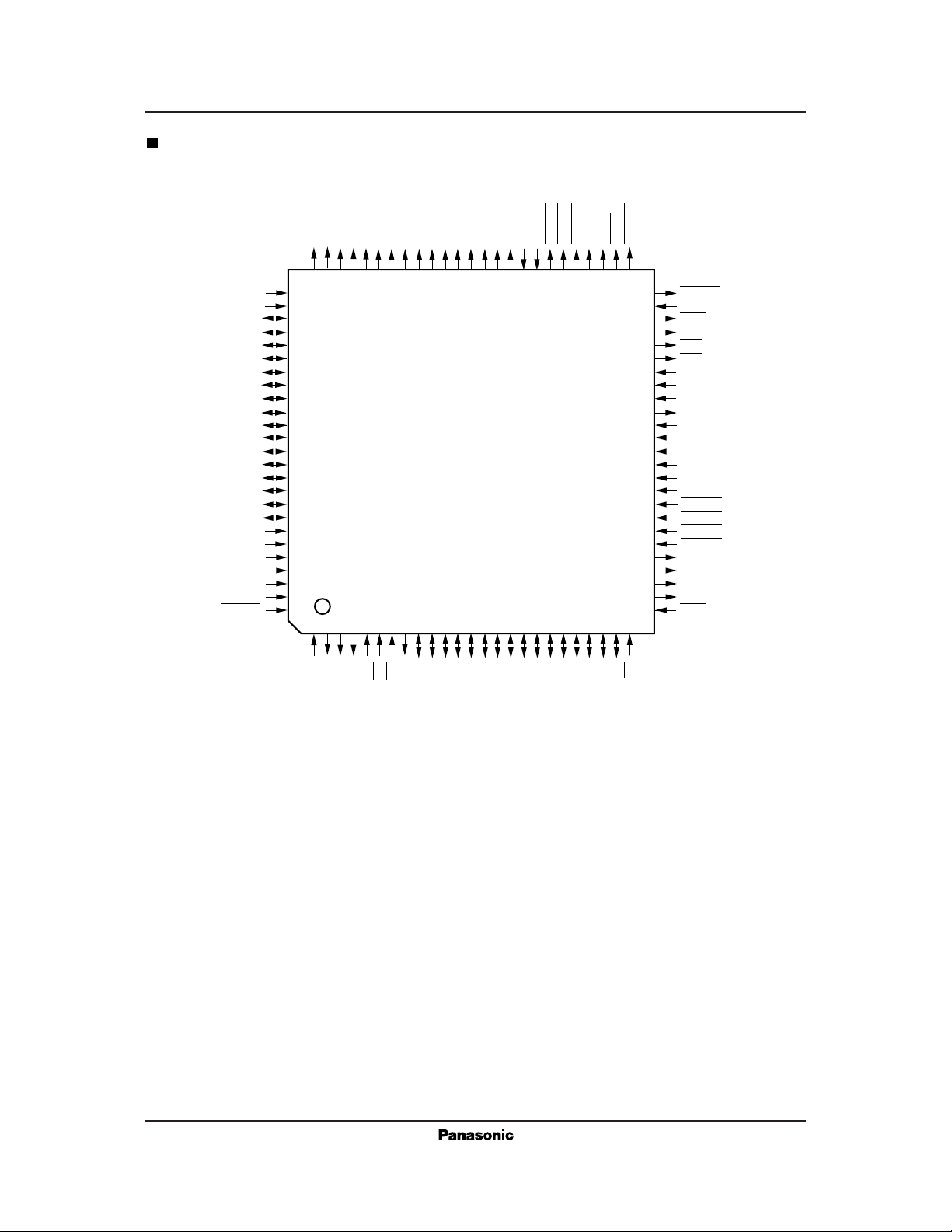
Pin Assignment
V
SS3
V
DD3
ID15
ID14
ID13
ID12
ID11
ID10
ID9
ID8
ID7
ID6
ID5
ID4
ID3
ID2
ID1
ID0
V
SS4
V
DD4
TEST3
TEST2
TEST1
TEST0
RESET
IA0
IA1
IA2
IA3
IA4
IA5
IA6
IA7
IA8
IA9
IA10
IA11
IA12
75747372717069686766656463626160595857565554535251
76
IA13
IA14
IA15
DD2VSS2
V
DACK1
DACK0
DSTR0
77
78
79
80
81
82
83
84
85
86
87
88
89
90
91
92
93
94
95
96
97
98
99
100
123456789
INTR1
INTR2
RD
HEX
INTR0
2SYSCLK
101112131415161718192021222324
WR
D15
D14
D13
D9D8D7D6D5D4D3D2D1D0CS
D12
D11
D10
SYSCLK
DSTR1
IMLE
IMUE
DCMP0
50
49
48
47
46
45
44
43
42
41
40
39
38
37
36
35
34
33
32
31
30
29
28
27
26
25
DCMP1
IREADY
IOW
IMW
IOR
IMR
DREQ0
DREQ1
IHACK
IHREQ
V
DD1
V
SS1
A0
A1
A2
A3
ACKD1
ACKD0
ACKC1
ACKC0
REQD1
REQD0
REQC1
REQC0
UBE
QFP100-P-1818
Page 3
For Communications Equipment MN86063
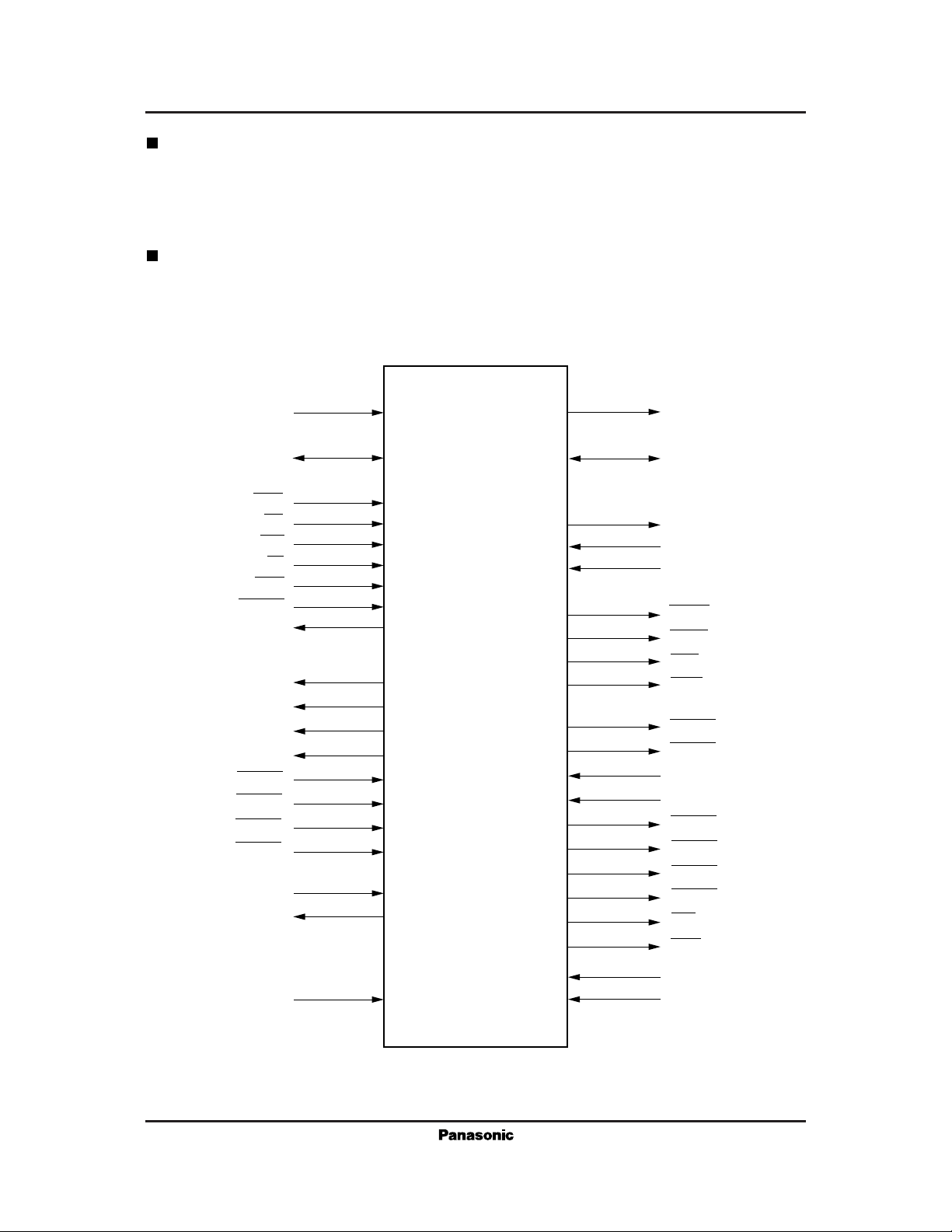
Pin Configuration
The MN86063 features two buses: the system bus, which is primarily used for transferring coded data to and from
a microprocessor and other components and the image bus, which is used for transferring image data to or from a
scanner, printer, or the like.
Pin Function Chart
The chip has a total of 100 pins: 39 for the system bus, 49 for the image bus, and 12 for testing, power supply, and
other purposes.
System bus pins
A0 to A3
D0 to D15
UBE
RD
WR
CS
HEX
RESET
INTR0 to 2
REQC0
REQC1
REQD0
REQD1
ACKC0
ACKC1
ACKD0
ACKD1
2SYSCLK
SYSCLK
MN8606X
Image bus pins
IA0 to 15
ID0 to 15
IHREQ
IHACK
IREADY
IMUE
IMLE
IMR
IMW
DSTR0
DSTR1
DREQ0
DREQ1
DACK0
DACK1
DCMP0
DCMP1
IOR
IOW
TEST0 to 3
VDD0 to 3
VSS0 to 3
Page 4
MN86063 For Communications Equipment
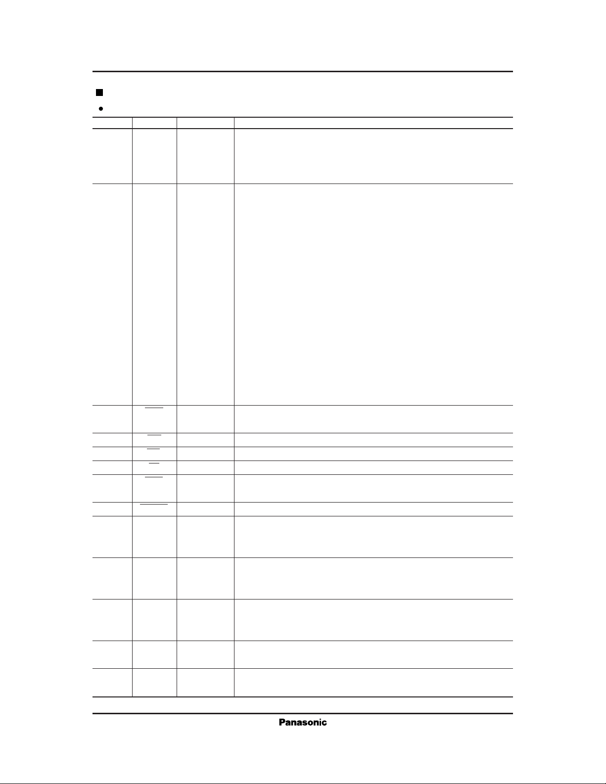
Pin Descriptions
System Bus
Pin No. Symbol I/O Function Description
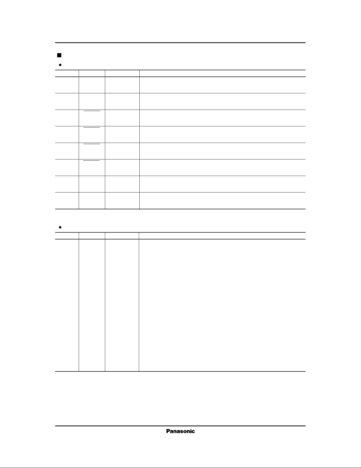
35 A3 I Address. Address bus for accessing internal registers
36 A2
37 A1
38 A0
9 D15 I/O Data. Data bus for bidirectional transfers over system bus
10 D14 Tristate
11 D13
12 D12
13 D11
14 D10
15 D9
16 D8
17 D7
18 D6
19 D5
20 D4
21 D3
22 D2
23 D1
24 D0
26 UBE I Upper byte enable. This input pin specifies whether the data from pins
D15–D8 is effective.
6 RD I Read. This input pin specifies a read from the specified register.
7 WR I Write. This input pin specifies a write to the specified register.
25 CS I Chip select. This input pin specifies access to a register.
1 HEX I Data bus width selection. This input pin specifies the width of the system
data bus: "0" for 16 bits; "1" for 8 bits.
100 RESET I Reset. This input pin resets the internal circuitry, clearing all registers.
2 INTR0 O Interrupt request 0. This output pin indicates an interrupt request
Open triggered by the cause given in interrupt register 0 (STIR0)
corrector
3 INTR1 O Interrupt request 1. This output pin indicates an interrupt request
Open triggered by the cause given in interrupt register 1 (STIR1)
corrector
4 INTR2 O Interrupt request 2. This output pin indicates an interrupt request
Open triggered by the cause given in DMA transfer interrupt register (DMIR).
corrector
27 REQC0 O DMA transfer output request 0. This output pin indicates a request for
data output on DMA channel 0.
28 REQC1 O DMA transfer output request 1. This output pin indicates a request for
data output on DMA channel 1.
Page 5
For Communications Equipment MN86063
Pin Descriptions (continued)
System Bus (continued)
Pin No. Symbol I/O Function Description
29 REQD0 O DMA transfer input request 0. This output pin indicates a request for data
input on DMA channel 0.
30 REQD1 O DMA transfer input request 1. This output pin indicates a request for data
input on DMA channel 1.
31 ACKC0 I DMA transfer output acknowledge 0. This input pin accepts the response
to a DMA transfer request with REQC0.
32 ACKC1 I DMA transfer output acknowledge 0. This input pin accepts the response
to a DMA transfer request with REQC1.
33 ACKD0 I DMA transfer input acknowledge 0. This input pin accepts the response
to a DMA transfer request with REQD0.
34 ACKD1 I DMA transfer input acknowledge 0. This input pin accepts the response
to a DMA transfer request with REQD1.
5 2SYSCLK I 2 system clock. This input pin accepts a clock signal with a frequency
twice that of the system clock.
8 SYSCLK O System clock. This output pin provides a clock signal with half the
frequency of 2SYSCLK.
Image Bus
Pin No. Symbol I/O Function Description
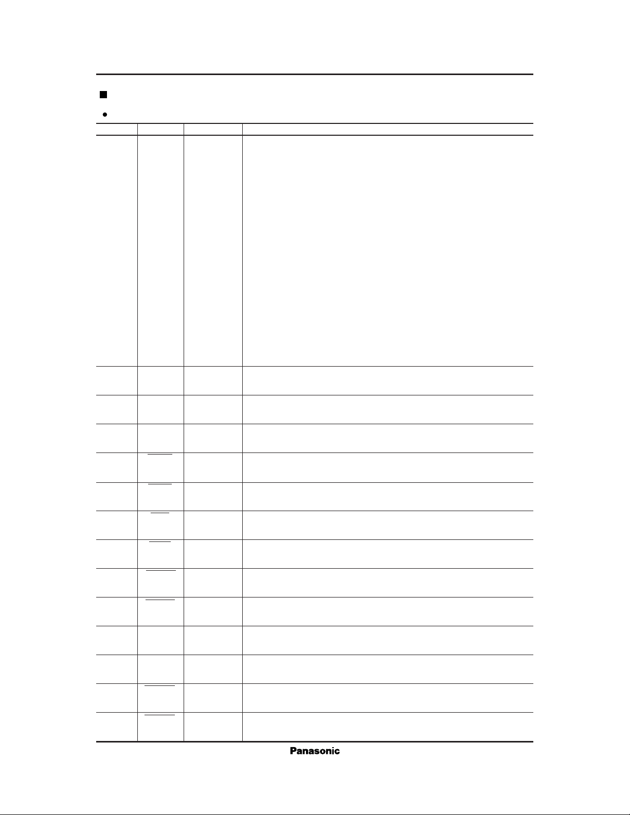
60 IA15 O Image address bus. These pins provide an address on the image data bus.
61 1A14 Tristate
62 IA13
63 IA12
64 IA11
65 IA10
66 IA9
67 IA8
68 IA7
69 IA6
70 IA5
71 IA4
72 IA3
73 IA2
74 IA1
75 IA0
Page 6
MN86063 For Communications Equipment
Pin Descriptions (continued)
Image Bus (continued)
Pin No. Symbol I/O Function Description
78 ID15 I/O Image data. These pins form a bus for bidirectional transfers of image data.
79 ID14 Tristate
80 ID13
81 ID12
82 ID11
83 ID10
84 ID9
85 ID8
86 ID7
87 ID6
88 ID5
89 ID4
90 ID3
91 ID2
92 ID1
93 ID0
41 IHREQ O Image bus request. This output pin indicates a request for control of the
image bus.
42 IHACK I Image bus acknowledge. This input pin indicates when the chip can seize
control of the image bus.
49 IREADY I Image data acknowledge. This input pin indicates the end of the read/
write operation.
52 IMUE O Image memory upper byte enable. This output pin specifies whether the
Tristate data from pins ID15–ID8 is effective.
53 IMLE O Image memory lower byte enable. This output pin specifies whether the
Tristate data from pins ID7–ID0 is effective.
45 IMR O Image memory read. This output pin indicates a read from the address on
Tristate the image address bus.
47 IMW O Image memory write. This output pin indicates a write to the address on
Tristate the image address bus.
55 DSTR0
54 DSTR1 O DMA start 1. This output indicates that the chip is ready for a DMA
44 DREQ0 I DMA request 0. This input pin indicates a request for a DMA transfer
43 DREQ1 I DMA request 1. This input pin indicates a request for a DMA transfer
56 DACK0 O DMA acknowledge 0. This output pin gives the response to the DREQ0
57 DACK1 O DMA acknowledge 1. This output pin gives the response to the DREQ1
O
DMA start 0. This output indicates that the chip is ready for a DMA
transfer from an I/O device to memory.
transfer from memory to an I/O device.
from an I/O device to memory.
from memory to an I/O device.
signal, initiating a DMA transfer from an I/O device to memory.
signal, initiating a DMA transfer from memory to an I/O device.
Page 7
For Communications Equipment MN86063
Pin Descriptions (continued)
Image Bus (continued)
Pin No. Symbol I/O Function Description
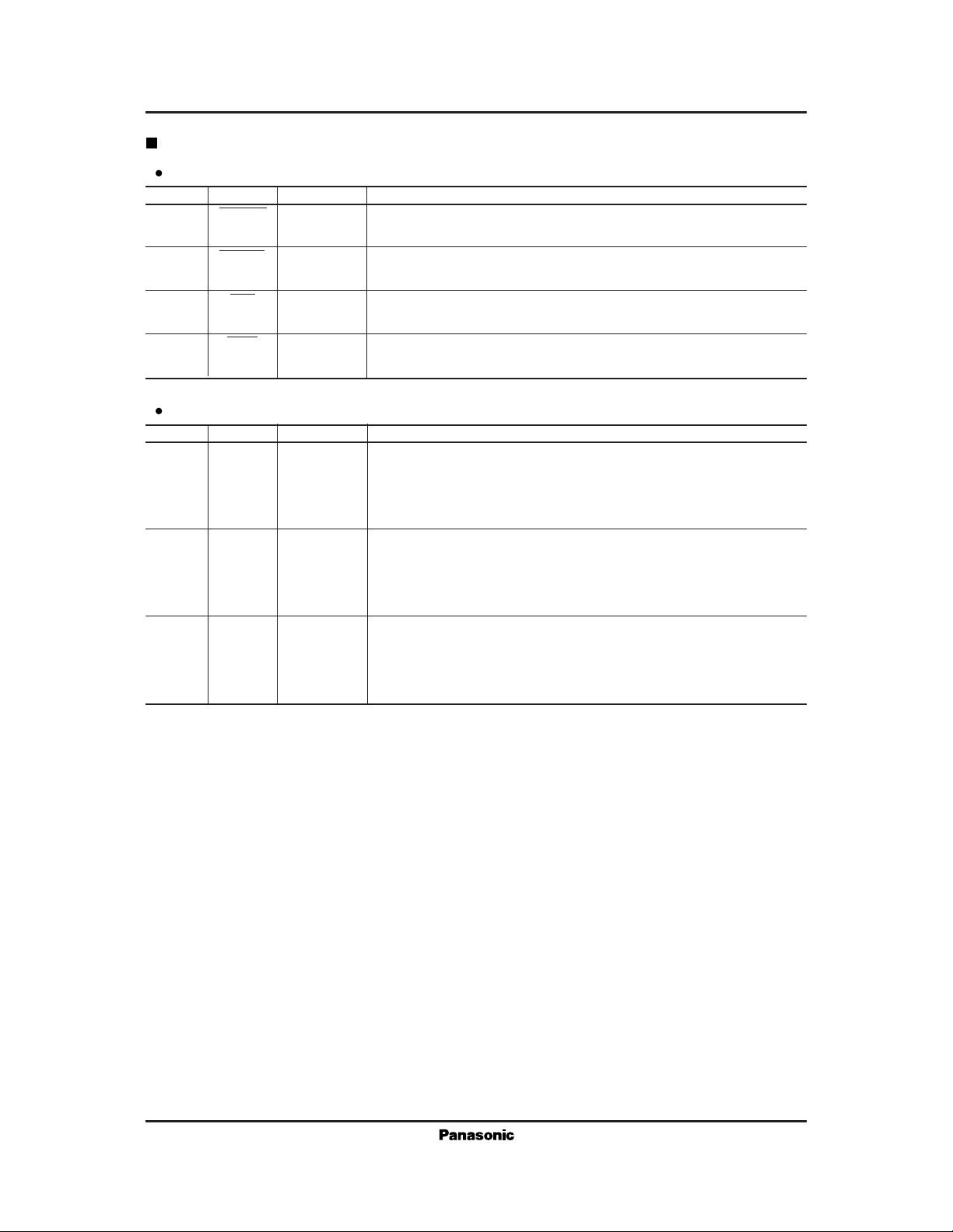
51 DCMP0 O DMA complete 0. This output pin indicates the successful completion of
the DMA transfer of 1 line of data from an I/O device to memory.
50 DCMP1 O DMA complete 1. This output pin indicates the successful completion of
the DMA transfer of 1 line of data from memory to an I/O device.
46 IOR O I/O device read. This output pin indicates a read from an I/O device
Tristate connected to the image address bus.
48 IOW O I/O device write. This output pin indicates a write to an I/O device
Tristate connected to the image address bus.
Power on Reset Circuit
Pin No. Symbol I/O Function Description
96 TEST3 I Test mode. Connect all these pins to the ground.
97 TEST2
98 TEST1
99 TEST0
40 V
59 V
77 V
95 V
39 V
58 V
76 V
94 V
DD1
DD2
DD3
DD4
SS1
SS2
SS3
SS4
I 5 volt power supply. Connect all these pins to a 5 volt power supply.
I Ground. Connect all these pins to the ground.
Page 8
MN86063 For Communications Equipment
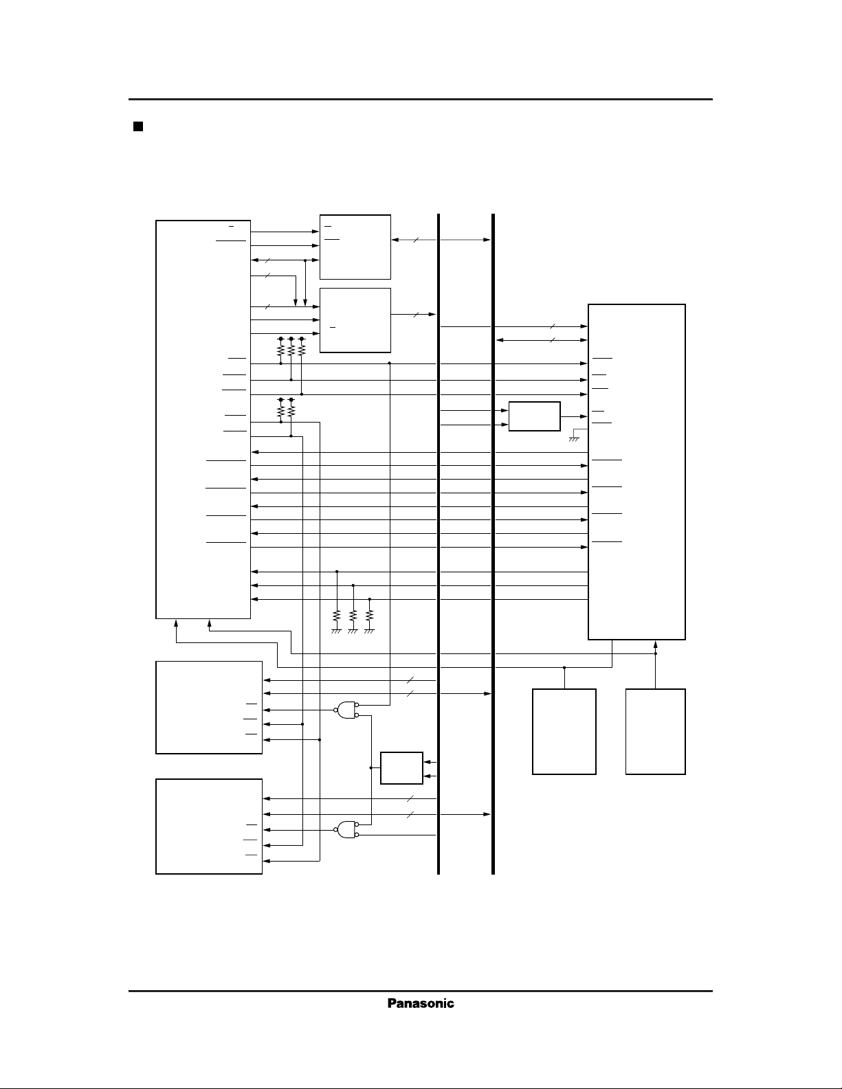
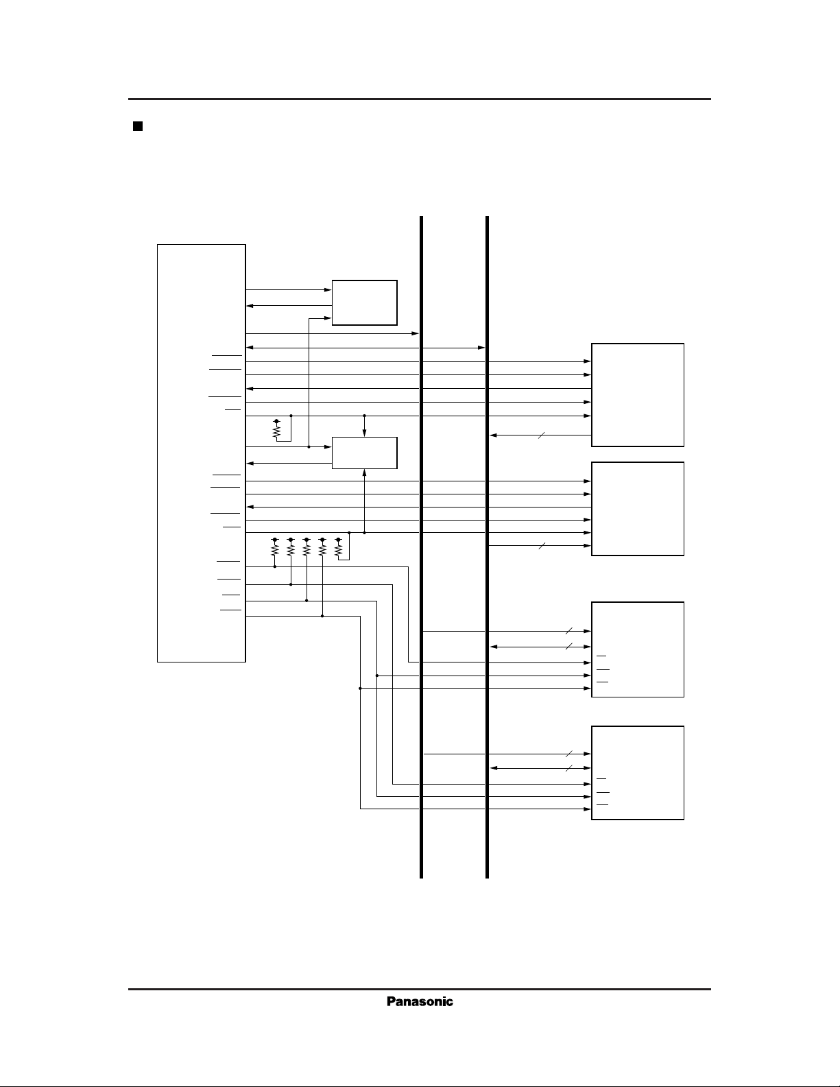
Application Circuit Example #1. Sample Connections to System Bus
(MPU)
BUFR/W
BUFEN
AD(0 to 15)
A(16 to 15)
BS(0 to 2)
ASTB
HDACK
UBE
IORD
IOWR
MRD
MWT
DMARQ0
DMAAK0
DMARQ1
DMAAK1
DMARQ2
DMAAK2
DMARQ3
DMAAK3
INTR0
INTR1
INTR2
RST
CLKIN
(Upper half of memory)
256-Kbit SRAM
A(0 to 14)
I/O(0 to 7)
(Lower half of memory)
256-Kbit SRAM
A(0 to 14)
I/O(0 to 7)
CS
WE
OE
CS
WE
OE
+5V
+5V
Address bus Data bus
74HC245
G
16
4
3
DIR
A
2 pieces
74HC573
D
C
OC
3 pieces
A(1 to 15)
D(8 to 15)
A(1 to 15)
D(0 to 7)
B
Q
15
Address
Decoder
15
16
23
A(0 to 3)
D(0 to 15)
BS(0 to 2)
A(4 to 19)
8
BS(0 to 2)
A(16 to 19)
8
A0
Address
Decoder
Crystal
oscillator
circuit
(20 MHz)
4
16
MN86063
A(0 to 3)
D(0 to 15)
UBE
RD
WT
CS
HEX
REQC0
ACKC0
REQC1
ACKC1
REQD0
ACKD0
REQD1
ACKD1
INTR0
INTR1
INTR2
2SYSCLK RESET
Power
on reset
circuit
Page 9
For Communications Equipment MN86063
Application Circuit Example #2. Sample Connections to Image Bus
MN86063
IA(0 to 15)
ID(0 to 15)
IHREQ
IHACK
DSTR0
DCMP0
DREQ0
DACK0
IOR
SYSCLK
IREADY
DSTR1
DCMP1
DREQ1
DACK1
IOW
IMUE
IMLE
IMR
IMW
+5V
Low-speed device
+5V
Bus
Arbiter
Timing
control
Address bus
Data bus
IA(1 to 15)
ID(8 to 15)
Scanner
8
Printer
8
(Upper half of memory)
256-Kbit SRAM
15
A(0 to 14)
8
I/O(0 to 7)
CS
WE
OE
IA(1 to 15)
ID(0 to 7)
(Lower half of memory)
256-Kbit SRAM
15
A(0 to 14)
8
I/O(0 to 7)
CS
WE
OE
Page 10
MN86063 For Communications Equipment
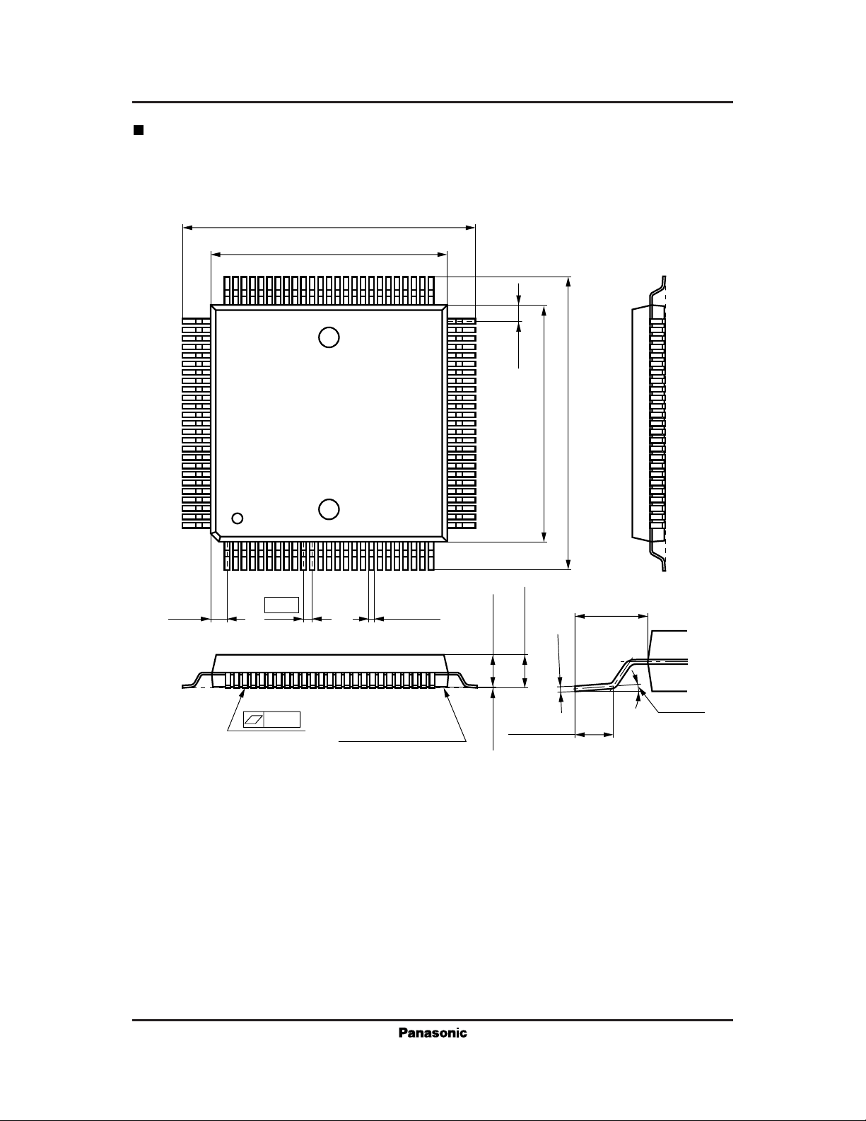
Package Dimensions (Unit: mm)
QFP100-P-1818
22.90±0.40
18.00±0.20
75 51
76
100
(1.20)
50
(1.20)
18.00±0.20
22.90±0.40
26
125
0.65
0.30±0.10
2.50±0.20
2.90 max.
–0.05
+0.10
(2.45
±0.20)
0.15
0.15
SEATING PLANE
(1.30
±0.20)
0.10±0.10
0 to 10°
 Loading...