

Page 1
For Video Equipment
MN676011NPS
NTSC Color Camera Synchronizing Signal Generator LSI
Overview
The MN676011NPS is a CMOS LSI that generates
NTSC color camera synchronizing signals as defined by
the EIA RS-170A standard.
It features a built-in 4f
(14.31818 MHz) crystal os-
SC
cillator circuit and divides that frequency to generate the
horizontal synchronizing signal f
synchronizing signal f
V
(15.7 kHz), the vertical
H
(60 Hz), and the composite
synchronizing signal.
It also divides the 4f
clock signal frequency by four
SC
to generate the color subcarrier frequency signals SC1
and SC2 and the burst signal gated with the burst flag
(BF) pulse.
It includes a vertical reset (VR) input pin for resetting
the leading edge of the vertical synchronizing pulse (VP)
with the falling edge of the input signal. It also includes
separate clock input pins for the color subcarrier frequency
signal circuits and the synchronizing signal circuits to
permit synchronization with such external synchronizing LSIs as the MN6761S.
Features
Power-saving CMOS synchronizing signal generator
(conformed to EIA RS-170A standard)
Built-in 14.31818 MHz clock generator
12 signal outputs including horizontal and vertical
synchronizing signals and color subcarrier
frequency signals (The vertical synchronizing signal
is available as the VP signal output.)
Pins for switching BLK signal pulse widths
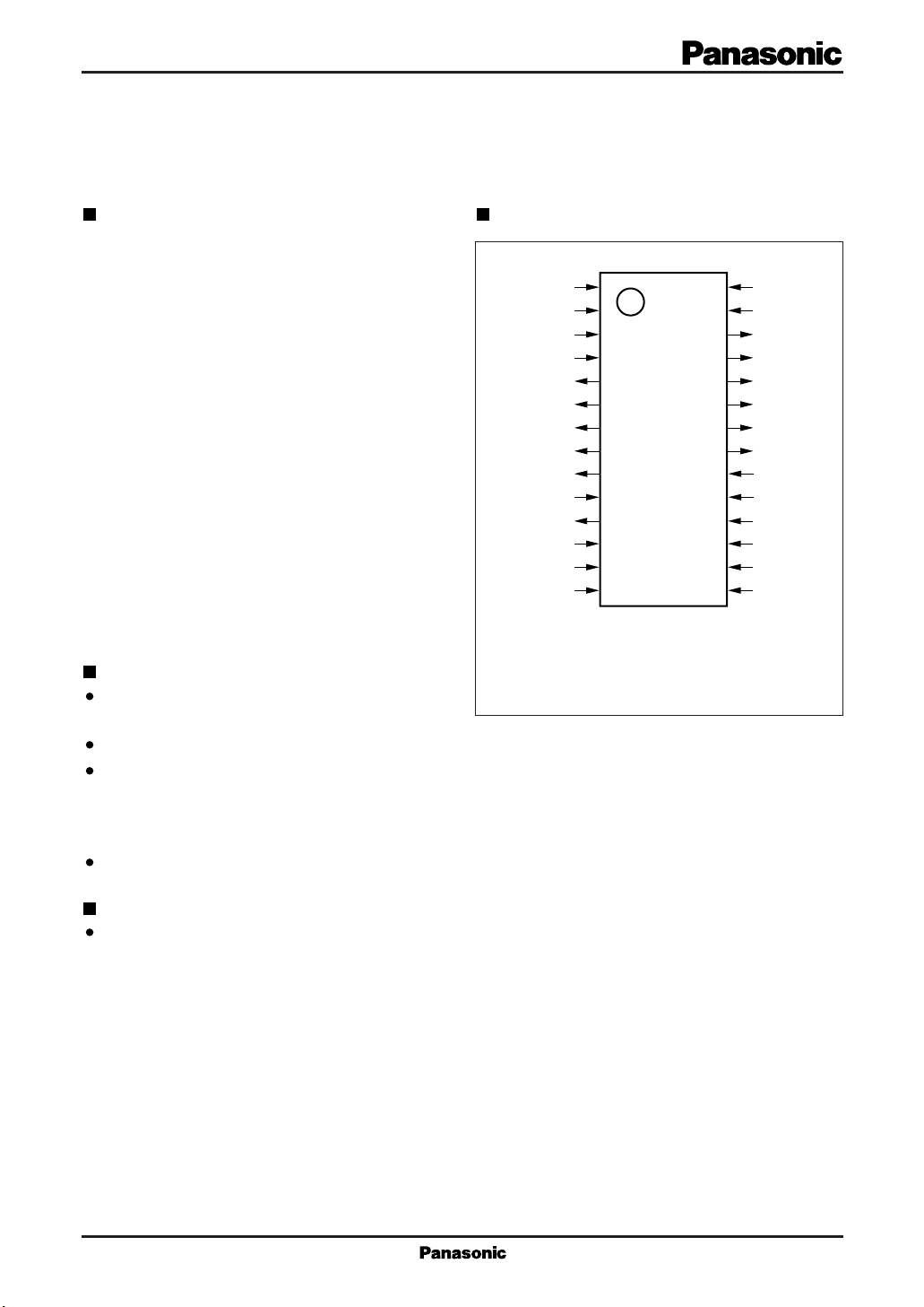
Pin Assignment
V
DD1
V
SS1
EX4fSCI
4fSCOSCI
4fSCOSCO
SC1
SC3
BSC
VPCO
EXT/INT
CP1
TEST
VR
EX910fHI
1
2
3
4
5
6
7
8
9
10
11
12
13
14
SOP028-P-0375
(TOP VIEW)
28
V
DD2
27
V
SS2
26
SYNC
25
VP
24
WHD
23
BLK
22
CP1V
21
CP2
20
WBLK
19
BF
18
SW1
17
SW3
16
SW3
15
SW4
Applications
Color video cameras
Page 2
MN676011NPS For Video Equipment
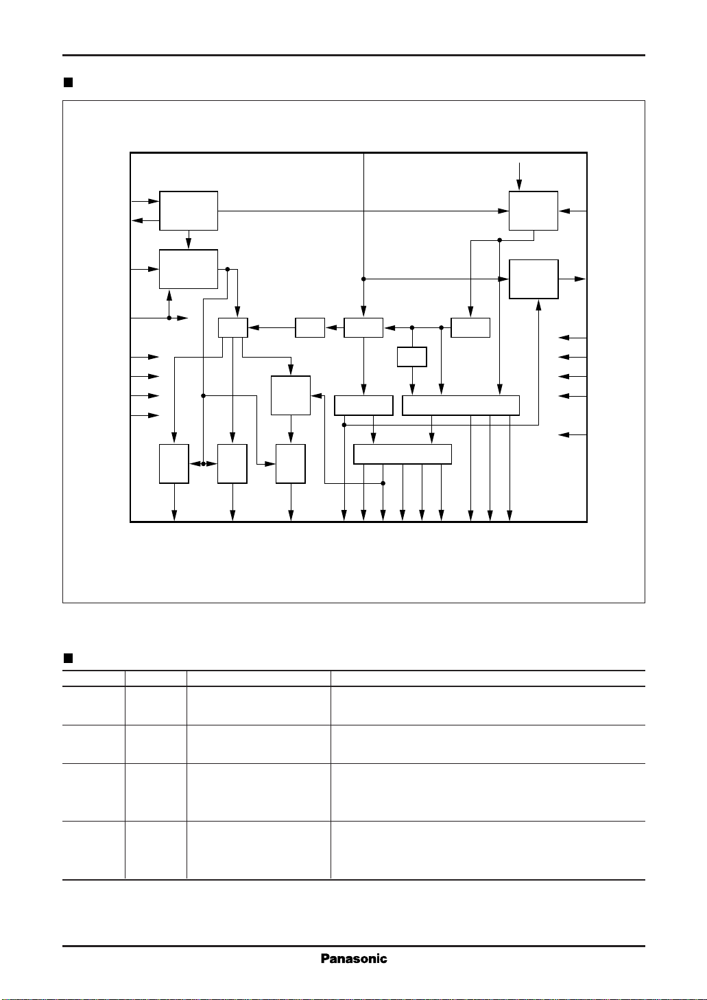
Block Diagram
VR
4f
4f
SC
OSCO
SC
EX4f
OSCI
SC
13
4
5
3
I
4f
SC
OSC
SC-CLK
SELECT
V-Reset
EXT/INT
HV-CLK
SELECT
PHASE
COMP.
14
9
EX910f
VPCO
I
H
EXT/INT
10
1
V
DD1
2
V
SS1
28
V
DD2
27
V
SS2
1/4
SC-Reset
Burst
Gate
1/4
1/525
f
V
V-Decoder H-Decoder
1/2
1/455
2f
f
H
H
910f
H
DDD
DFF
6
SC1
DFF
CK CK
7
SC2
DFF
8
BSC
Composite Decoder
25
19
22
BF
VP
CP1V
20
WBLK
23
BLK
26
SYNC
24
WHD
11
CP1
21
CP2
Pin Descriptions
Pin No. Symbol Pin Name Function Description
1V
2V
28 V
27 V
DD1
SS1
DD2
SS2
Power supply "H" level power supply (Connect this pin to +5.0 ±0.5 V.)
Power supply for color subcarrier frequency signal circuits
Power supply "L" level power supply (Connect this pin to 0 V.)
Power supply for color subcarrier frequency signal circuits
Power supply "H" level power supply (Connect this pin to +5.0 ±0.5 V.)
Power supply for horizontal and vertical synchronizing
signals
Power supply "L" level power supply (Connect this pin to 0 V.)
Power supply for horizontal and vertical synchronizing
signals
18
SW1
17
SW2
16
SW3
15
SW4
12
TEST
Page 3
For Video Equipment MN676011NPS
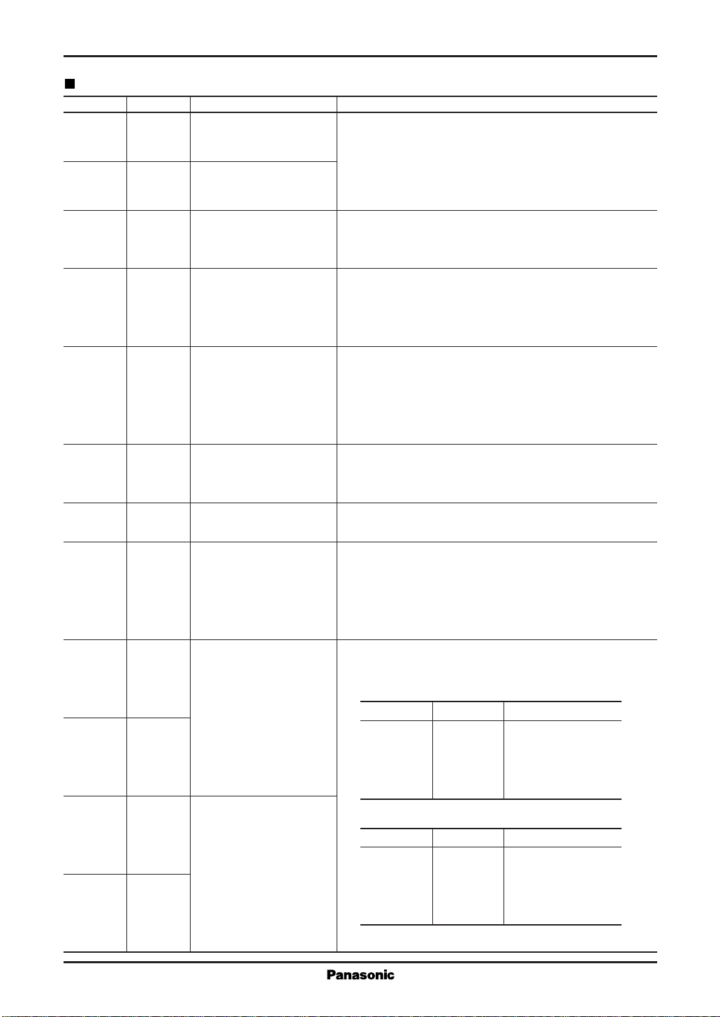
Pin Descriptions (continued)
Pin No. Symbol Pin Name Function Description
44f
OSCI Crystal oscillator
SC
input
54f
OSCO Crystal oscillator
SC
output
3 EX4f
14 EX910f
I External clock input Color subcarrier frequency (4fSC) input
SC
I External clock input External 910fH (14.31818 MHz) input for horizontal and
H
10 EXT/INT External/internal
synchronization switch
input
13 VR Vertical reset input Falling edge input resets the leading edge of the vertical
12 TEST Test input Test input Keep this pin at "H" level.
9 VPCO Phase comparator This pin gives the results of comparing the phases of the
output falling edge of the VR input and rising edge of the VP
18 SW1
Connect these pins to a 14.31818-MHz crystal oscillator
through capacitors appropriate for V
SS1
.
"L" level input to the EXT/INT pin (which includes a builtin feedback resistor) produces oscillation; "H" level input
stops it.
"H" level input to the EXT/INT pin enables external clock
input. If this pin is not used, keep it at "L" level.
vertical synchronizing signals
"H" level input to the EXT/INT pin enables external clock
input. If this pin is not used, keep it at "L" level.
This pin switches the chip between external and internal
synchronization modes.
"H" level input produces external synchronization;
"L" level, internal synchronization.
Incorporating pull-down resistor.
synchronizing signal (VP).
The pin includes a built-in pull-up resistor.
The pin includes a built-in pull-up resistor.
output.
The output is at "H" level when the VR leads the VP and is
at "L" level when the VR trails the VP.
These pins control the widths of H-BLK and V-BLK pulses.
17 SW2
16 SW3
15 SW4
H-BLK pulse width
selection
V-BLK pulse width
selection
SW1 SW2 H-BLK (µs)
L L 10.69
H L 10.82
L H 10.97
H H 11.10
SW3 SW4 V-BLK (H)
LL 19
HL 20
LH 21
HH 21
Page 4
MN676011NPS For Video Equipment
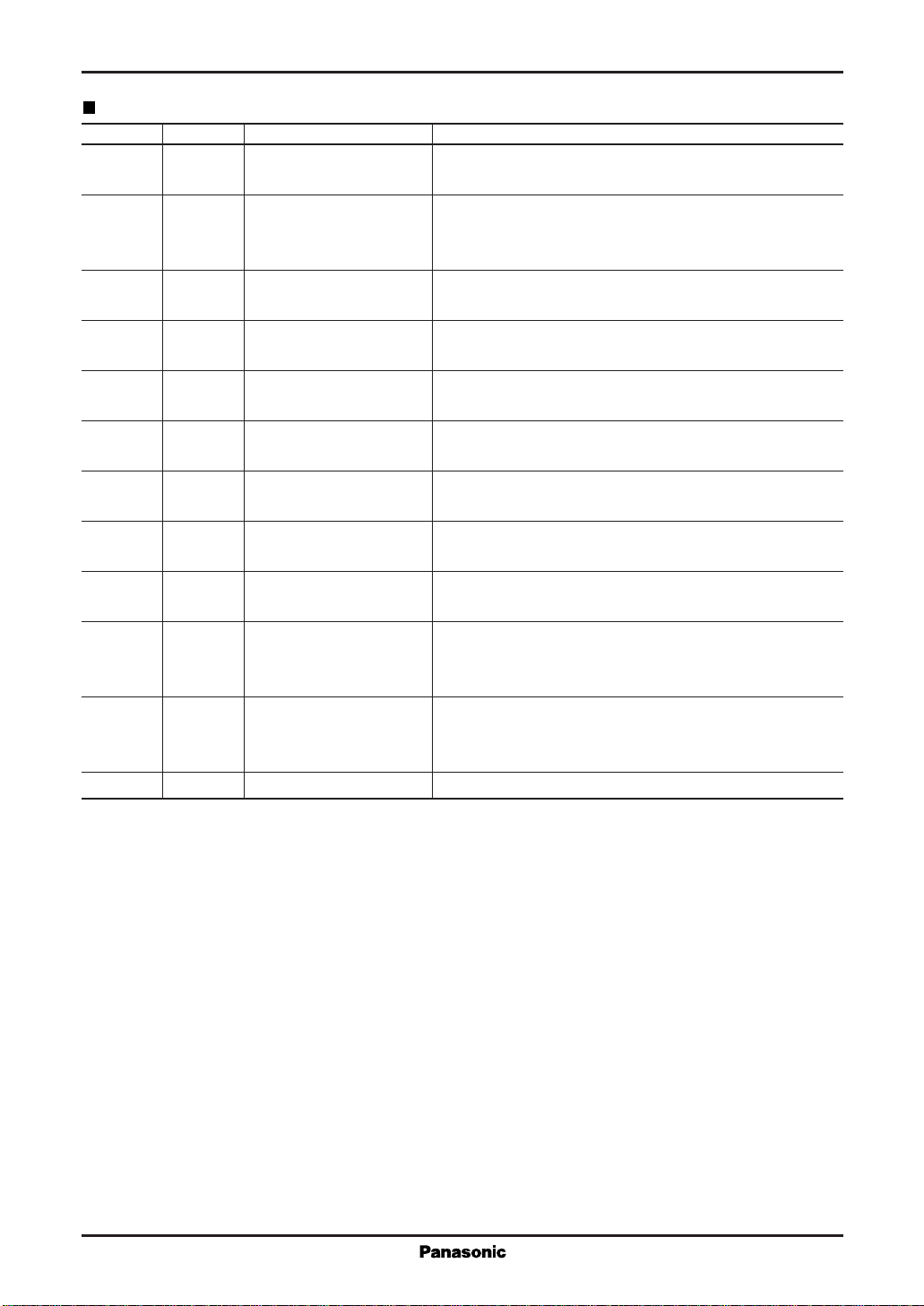
Pin Descriptions (continued)
Pin No. Symbol Pin Name Function Description
6 SC1 f
7 SC2 f
8 BSC Burst output Burst output signal
26 SYNC Composite synchronizing Composite synchronizing signal
25 VP Vertical synchronizing Vertical synchronizing signal output (width: 3H)
24 WHD Wide HD output Wide HD signal
23 BLK Composite blanking Composite blanking signal
22 CP1V Composite clamp pulse Composite pulse for black level playback
21 CP2 Clamp pulse output Clamp pulses for luminance and color difference signals
20 WBLK Composite wide Composite wide blanking signal
19 BF Burst flag output Gate signal for color subcarrier frequencies
11 CP1 Clamp pulse output Pulse for black level playback
(R-Y) output Color subcarrier frequency signal (3.58 MHz) formed by
SC
dividing the crystal oscillator signal (4fSC) by four.
(B-Y) output Color subcarrier frequency signal (3.58 MHz) formed by
SC
dividing the crystal oscillator signal (4f
) by four.
SC
This signal lags SC1 by 90°.
If SC1 is the 180° signal, BSC is the 0° signal.
signal output
signal output
Preblanking signal with pulse width of 9.71 µs
signal output See the entries for SW1–SW4 for the pulse width.
output
Horizontal deflection start pulses
blanking output This signal provides a horizontal blanking interval of
26.89 µs and a vertical blanking interval of 134.5H
The pulse width is 2.51 µs with the vertical interval (9H)
dropped out.
Page 5
For Video Equipment MN676011NPS
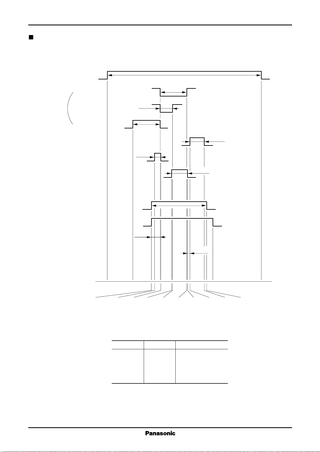
H Decoder Pulse Timing Diagram
WBLK
Sync
BF
CP1, CP1V
CP2
WHD
BLK
F.Porch
H.Sync
EQ
V.SER
2.23
1.05
1.47
4.68
26.89
4.75
Unit: µs
2.51
2.79
9.71
Sync to BF
–9.15
–1.47 – 0.91
0.56
–4.68
0.14
SW1 SW2 H-BLK (µs)
L L 10.69
H L 10.82
L H 10.97
H H 11.10
0
2.23 4.75 4.89
2.10
5.31
17.74
7.82 8.24
Page 6
MN676011NPS For Video Equipment
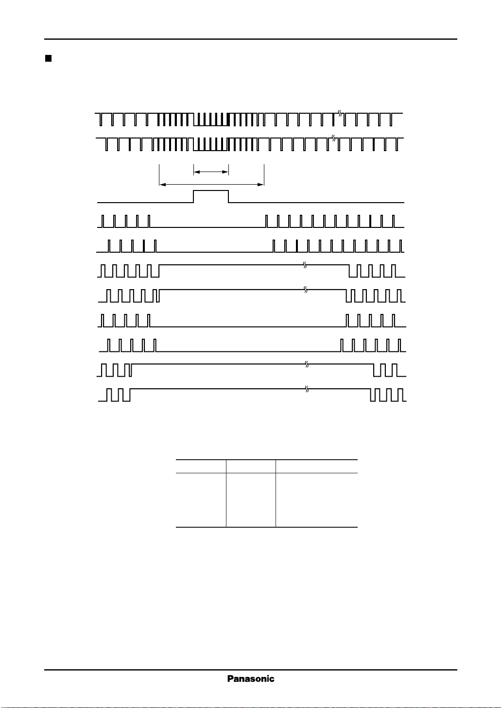
Pulse Timing Diagram for Composite and Vertical Synchronizing Signals
525
Sync
VP
{
12
262
{
HS EQ VS EQ HS
{
3H
9H
{
{
{
(
Field
ODD
EVEN
)
BF
BLK
CP1V
WBLK
{
{
{
{
489
227
524
524
262
262
134.5H+19.3µs
134.5H+7.6µs
SW3 SW4 V-BLK (H)
LL 19
HL 20
LH 21
HH 21
ODD
EVEN
ODD
EVEN
ODD
EVEN
101
ODD
362
EVEN
Page 7
For Video Equipment MN676011NPS
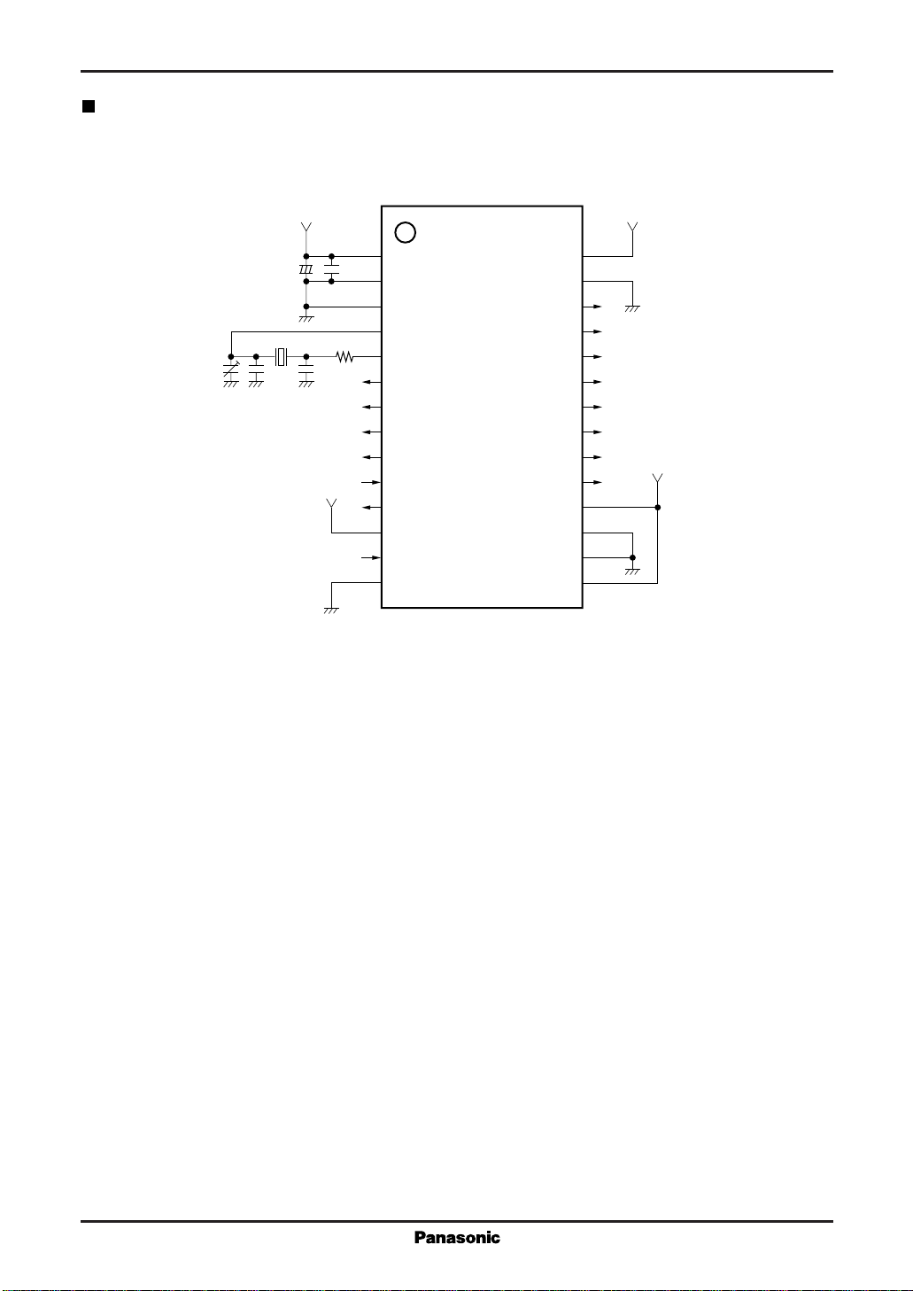
Application Circuit Example
20pF
5V
+
10µF
10pF 18pF
14.31818MHz
10000pF
1kΩ
1
2
3
4
5
6
7
8
9
10
11
12
13
14
VDD1
1
V
SS
EX4f
SC
OSCI
4f
SC
OSCO
4f
SC
SC1
SC2
BSC
VPCO
EXT/INT
CP1
TEST
VR
EX910f
5V
28
2
V
DD
27
2
V
SS
SYNC
VP
26
25
I
24WHD
23BLK
CP1V
22
CP2
21
WBLK
20
BF
19
SW1
18
SW2
17
SW3
16
SW4
I
H
15
5V
Page 8
MN676011NPS For Video Equipment
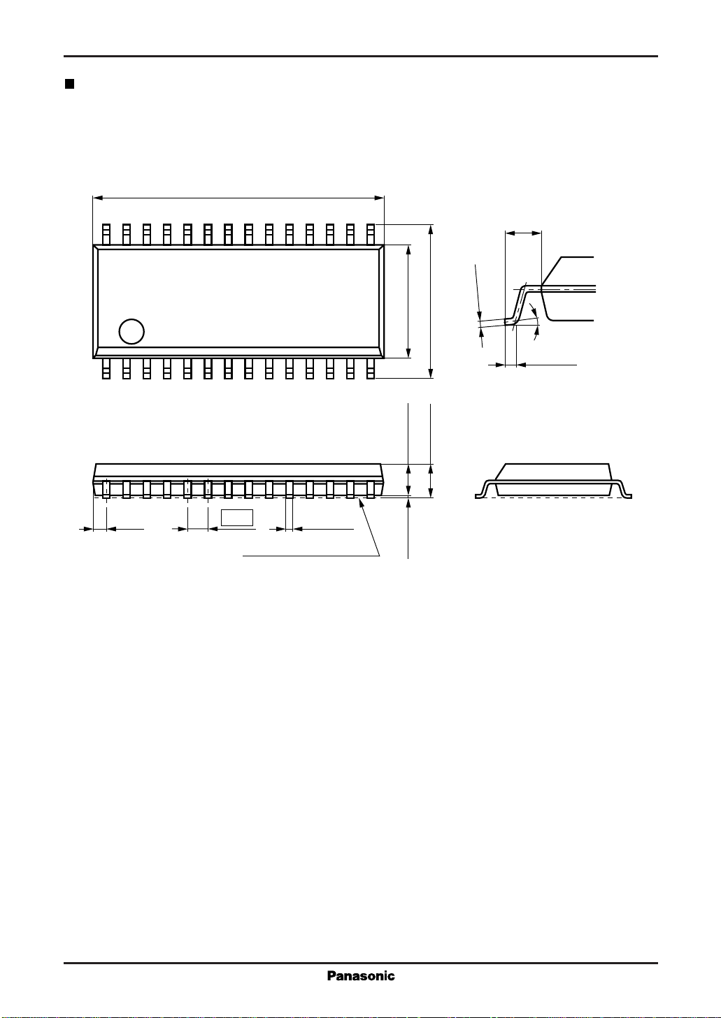
Package Dimensions (Unit: mm)
SOP028-P-0375
17.80
±0.20
28
15
0.05
-
+0.10
1.10±0.20
0.15
7.20±0.202.00±0.200.10±0.10
0 to 10°
0.30min.
114
2.40max. 9.40±0.30
(0.65) 0.40
1.27
±0.10
SEATING PLANE
 Loading...