

Page 1
For Communications Equipment
MN86157
Shading Correction LSI
Overview
The MN86157 contains a 7-bit A/D converter for use
in correcting, at the bit level, shading distortion for signals from image sensors, optics, and similar sources.
It uses external RAM to support adaptive correction
that responds to changes in distortion patterns. It also uses
ROM to provide fixed correction when a white reference
plane signal is not available.
The chip is also usable as a stand-alone A/D converter.
Features
Choice of correction range (50% or 75%) depending
on extent of shading distortion
Parallel A/D converter functions
Resolution: 7 bits
Non-linearity: ±1/2 LSB
Conversion speed: max. 5 MHz
Note: This is the guaranteed design value for the
chip used as a stand-alone A/D converter. The
guaranteed value at shipment is ±3 LSB
Ability to start and stop clock in the middle of a line
to support CdS contacting image sensors and other
devices with variable scanning rates
Overflow pin that simplifies task of adding auto
background control (ABC) circuit
Single 5 volt power supply
Guaranteed TTL levels for input
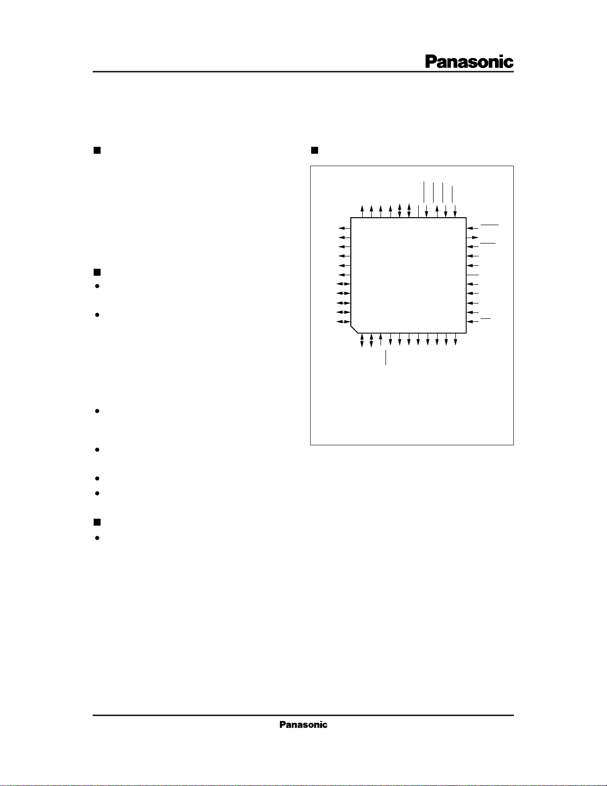
Pin Assignment
A6A7A8A9A10
A5
A4
A3
A2
A1
A0
D0
D1
D2
D3
D4
3332313029282726252423
34
35
36
37
38
39
40
41
42
43
44
1234567891011
D5
D6
ROS
QFP044-P-1010
A11
N.C.
DB5
DB4
MOE
OVF/DB6
(TOP VIEW)
MODE
ENBO
DB3
DB2
CKSH
ENBI
22
21
20
19
18
17
16
15
14
13
12
DB1
DB0
SHST
R/W
INHI
V
SS
V
DD
N.C.
VREFL
VIN
VREFH
V
DD
OE
Applications
Facsimile equipment
Page 2
MN86157 For Communications Equipment
Block Diagram
DB0 to 5
OE
12
7
6
Selector
7
Multiplier
7
7
SHADING CORRECTOR LSI
Selector
OVF/DB6
5
ROS
3
Distortion-
Coefficient
ROM
DDVDD
V
13
18
7
7
SS
V
19
Selector
D0 to 6
7
RAM or ROM
A0 to 11
VR
7
VREFH
ADC
VREFL
7
Controller
2423222026
INHI
ENBI
SHST
CKSH
MODE
25
ENBO
12
21
R/W
4
MOE
Page 3
For Communications Equipment MN86157
MN86157 Block Configuration
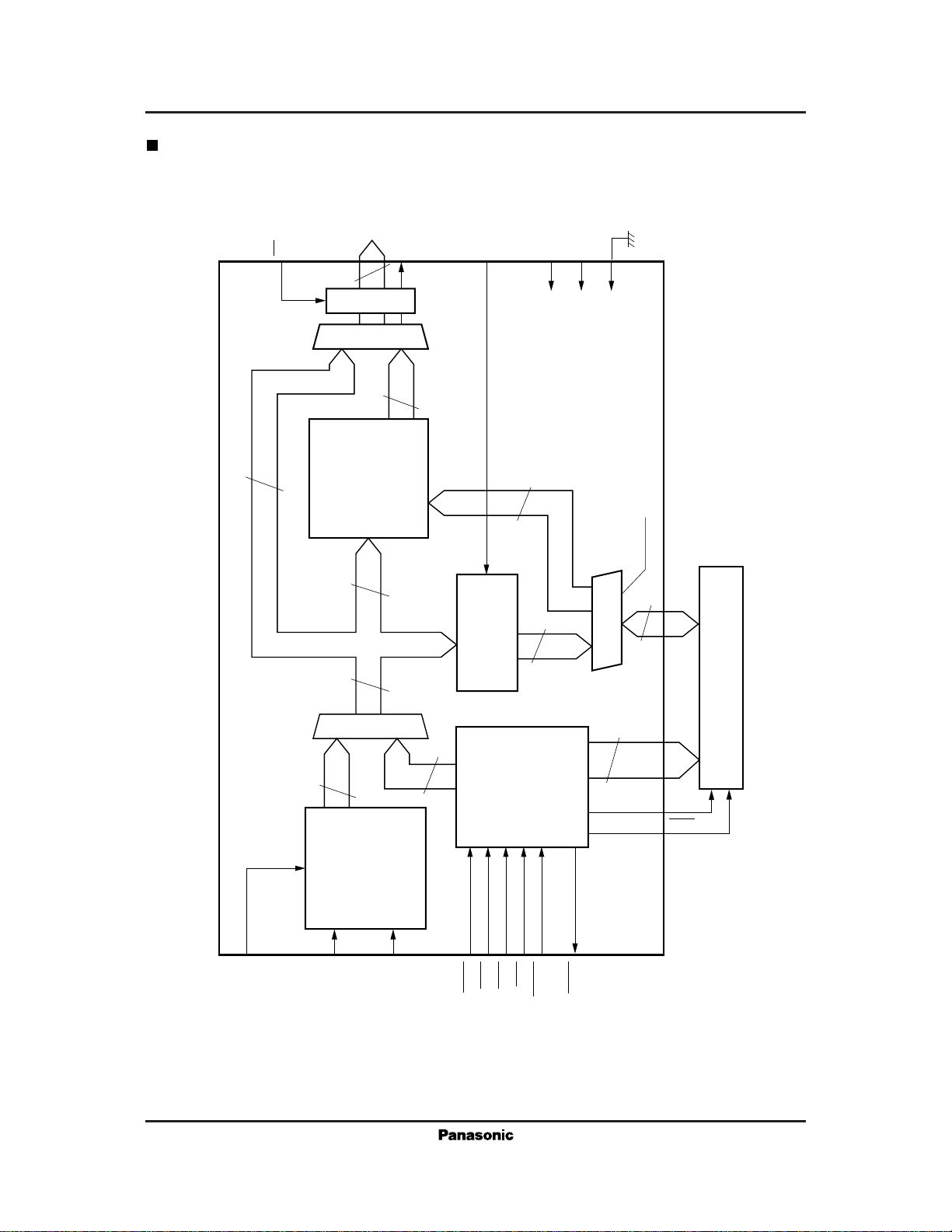
The MN86157 consists of four basic blocks: (1) A/D
converter, (2) distortion coefficient mapping ROM, (3)
multiplier, and (4) controller.
The following are brief descriptions of each block.
(1) A/D converter
This uses comparison with the reference voltages
to convert the scanner's image data signal from
the VIN pin to a 7-bit digital output.
(2) Distortion coefficient mapping ROM
This constitutes a look-up table for converting the
A/D converter output to a final value for storage
in the external RAM.
(3) Multiplier
This provides high-speed parallel multiplication
of 7 × 7 bits data.
(4) Controller
This controls operation of the shading correction
circuits, the A/D converter, and interface to
external ROM or RAM.
Operation
Shading correction (MODE pin at "H" level)
• Fixed distortion coefficients (external memory
is ROM)
This configuration provides 6-bit corrected data
using fixed distortion coefficients stored in an
external ROM and thus invariant.
• Adaptive distortion coefficients (external
memory is RAM)
This configuration provides 6-bit corrected data
using distortion coefficients, stored in external
RAM, that the chip constantly updates using
white reference plane line training.
• Pixels per line
The chip supports line lengths up to 4096 pixels
with a built-in 12-bit address counter supporting
interfaces to two 2
equivalent of a 2732 ROM (2
• Input clock
The chip uses an input clock signal with a
frequency twice that of the image clock.
• Selecting correction range
The ROS pin provides a choice of two correction
ranges and consequently correction precisions.
11
× 8-bit RAM chips or the
12
× 8 bits).
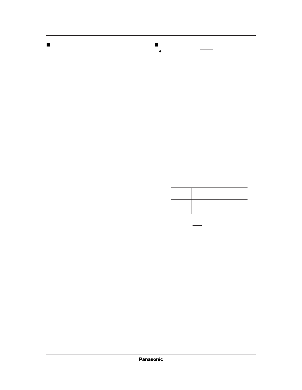
ROS
Correction Correction
Range Precision
H 50% ±1.5%
L 75% ±3.0%
• Correction start/stop function
Pulling the INHI pin to "L" level in the middle
of a line suspends correction and maintains the
output data at its current value. Returning the
pin to "H" level restarts correction.
• Auto clamp and overflow functions for output
data
If the image input signal level exceeds the white
reference plane level, the chip clamps the output
data at the full-scale value (3F
) and drives the
H
overflow pin (OVF) at "H" level.
Page 4
MN86157 For Communications Equipment
Stand-alone A/D converter (MODE pin at "L" level,
A10 pin at "L" level)
• In this configuration, the chip functions as a parallel A/D converter consisting of 128 chopper
comparators.
Resolution: 7 bits
Non-linearity: ±1/2 LSB
Conversion speed: max. 5 MHz
Analog input range: 3V p-p
(V
5V)
DD
• Clock mode selection
The A11 pin provides a choice of two clock
modes.
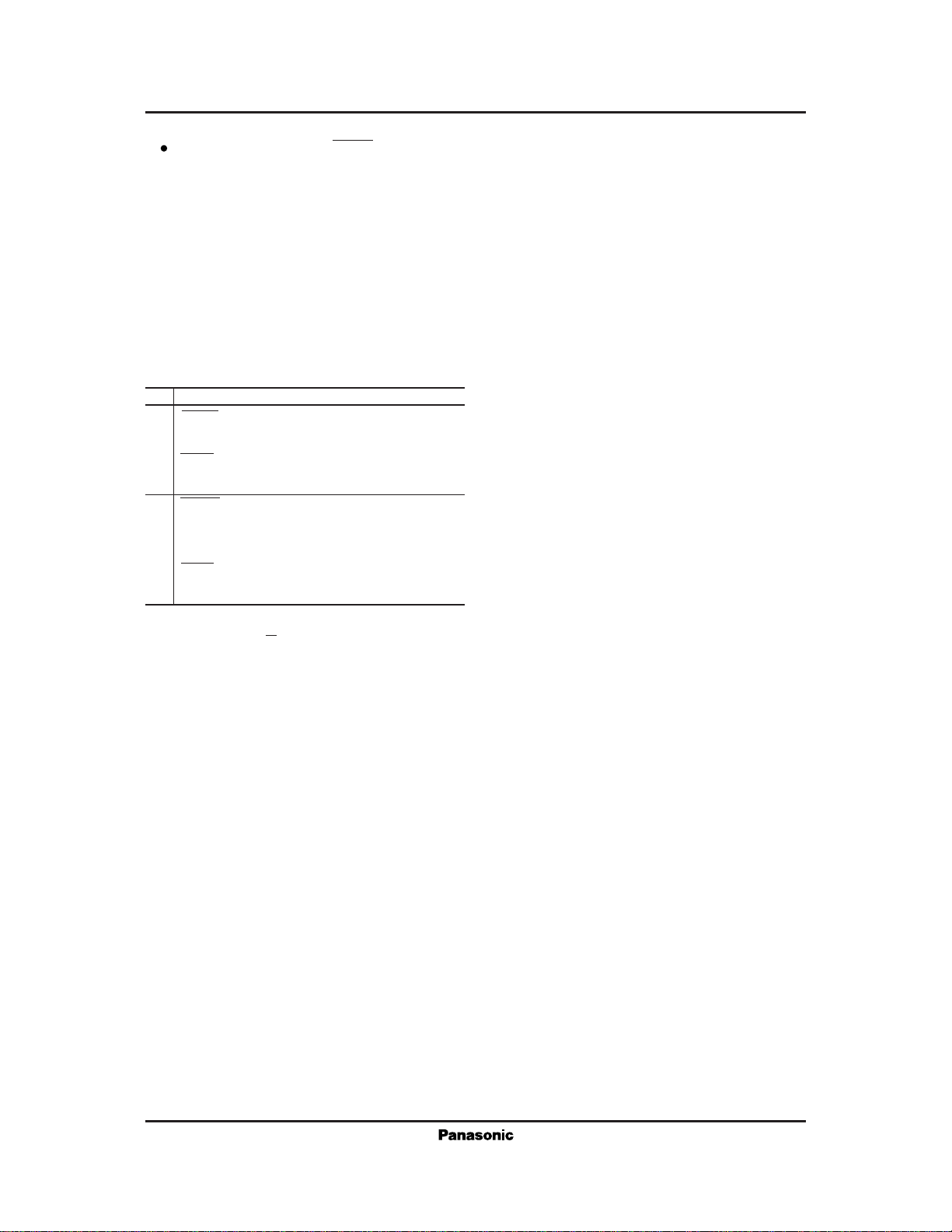
A11 Input Clock Conditions
CKSH: Supply a clock signal with a frequency
L
SHST: Supply the A/D start signal for use in
twice that of the input image clock. *
synchronizing phase.
CKSH: Supply a clock signal with a
frequency twice that of the input
H
image clock. *
2
ENBI: Supply a clock signal with the same
frequency as the input image clock.
Notes
1
: ENBI
*
2
: SHST: Keep this pin at "H" level.
*
1
Page 5
For Communications Equipment MN86157
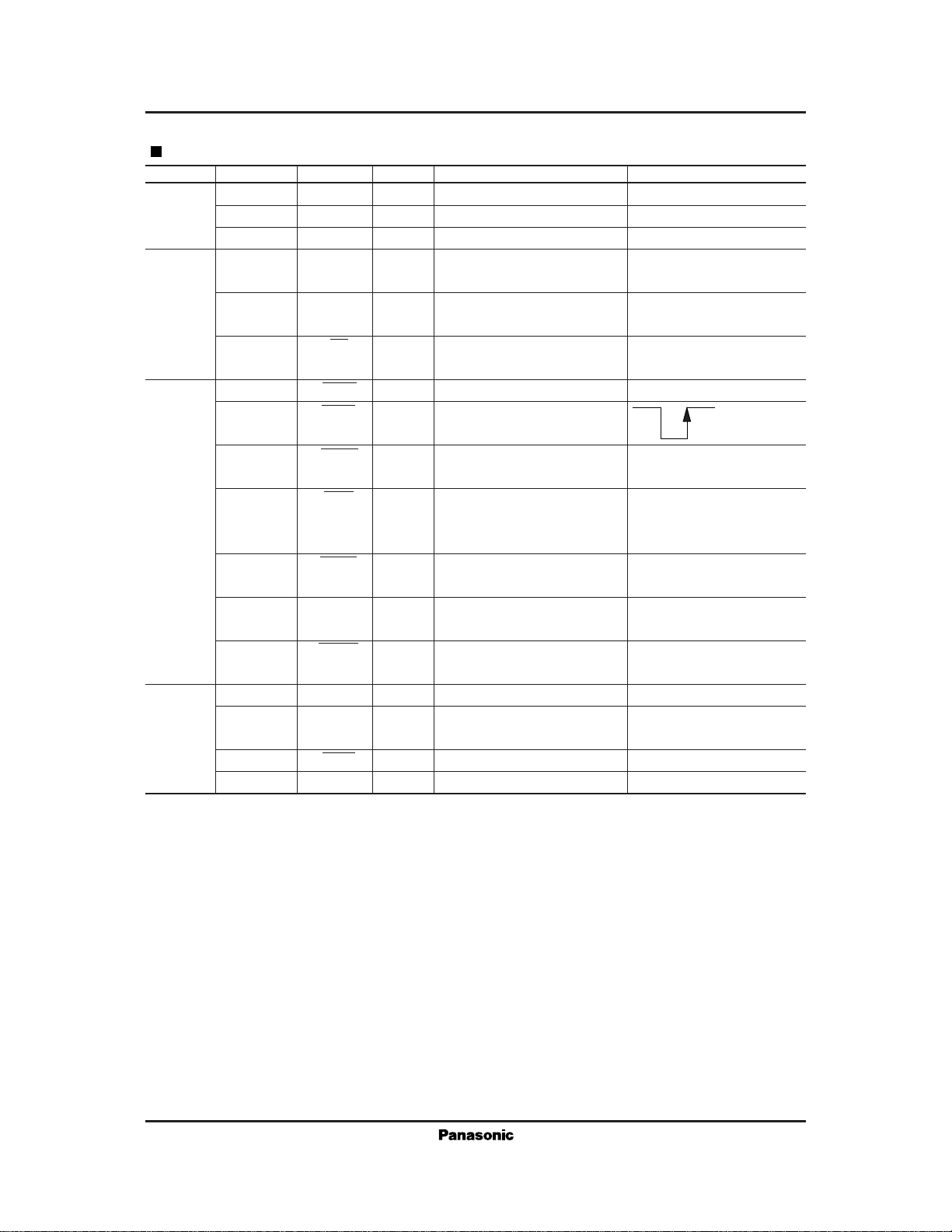
Pin Descriptions
Parameter Pin No. Symbol I/O Function Description Remarks
A/D 15 VIN I Analog image signal input
converter 14 VREFH — Reference voltage input "H" level reference voltage input
block 16 VREFL — Reference ground "L" level reference voltage input
MULT 11 to 6 DB 0 to 5 O Corrected image signal output MODE: H
converter /A/D converter data output /MODE: L
block 5 OVF/DB6 O Corrected image signal overflow MODE: H
output/A/D converter data output /MODE: L
12 OE I Output enable signal input H: Pins are high-impedance;
for DB0 – DB5 and OVF L: Pins provide output
CTL 23 ENBI I Enable signal input for single line
converter 22 SHST I Start input for reading white Low pulse
block reference signal signals start.
24 CKSH I Clock signal input The frequency must be twice
that of the image clock.
20 INHI I Signal for suspending correction in H: Normal correction
the middle of a line and holding operation;
the output at the current value L: Stop and hold
25 ENBO O Enable signal for corrected
image data output
3 ROS
26 MODE
RAM
/ROM
IO
converter 21 R/W O RAM read/write signal
block 4 MOE O RAM/ROM output enable signal
39 to 28 A 0 to 11 O RAM/ROM address output
40 to 44,
1, 2
D 0 to 6 I/O RAM/ROM data I/O
I Correction range selection
I Operating mode selection
H: 50% correction;
L: 75% correction
H: Shading correction;
L: A/D conversion only
Page 6
MN86157 For Communications Equipment
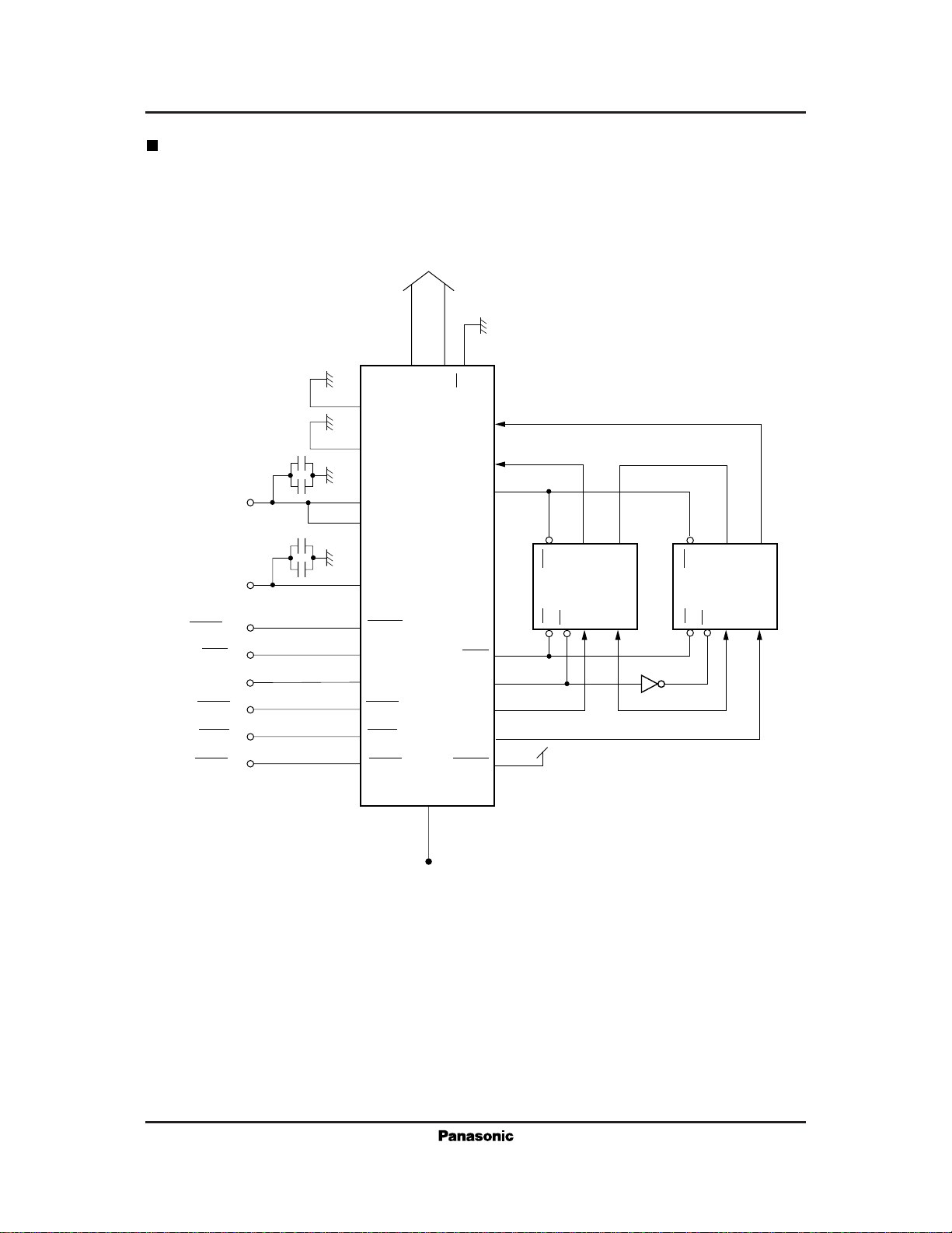
Application Circuit Example #1: Using RAM
DB0 to 5(O)
to
DB0
OE
D6
to
D0
RAM
(4 Kilowords × 8 bits)
RAM
(4 Kilowords × 8 bits)
V
SS
GND
DB5
AV
DD
5V
VREF
5V
ENBO(O)
INHI(I)
ROS (H/L)
SHST(I)
ENBI(I)
CKSH(I)
V
DD
V
DD
AG AG AG AG
VR
MN86157
ENBO
ROS
SHST
ENBI
CKSH MODE
VIN
PIX
R/W
MOE
A11
A10
to
A0
D0
OE WECSA0
to
D6
to
A10
OE WECSA0
D0
to
D6
to
A10
Page 7
For Communications Equipment MN86157
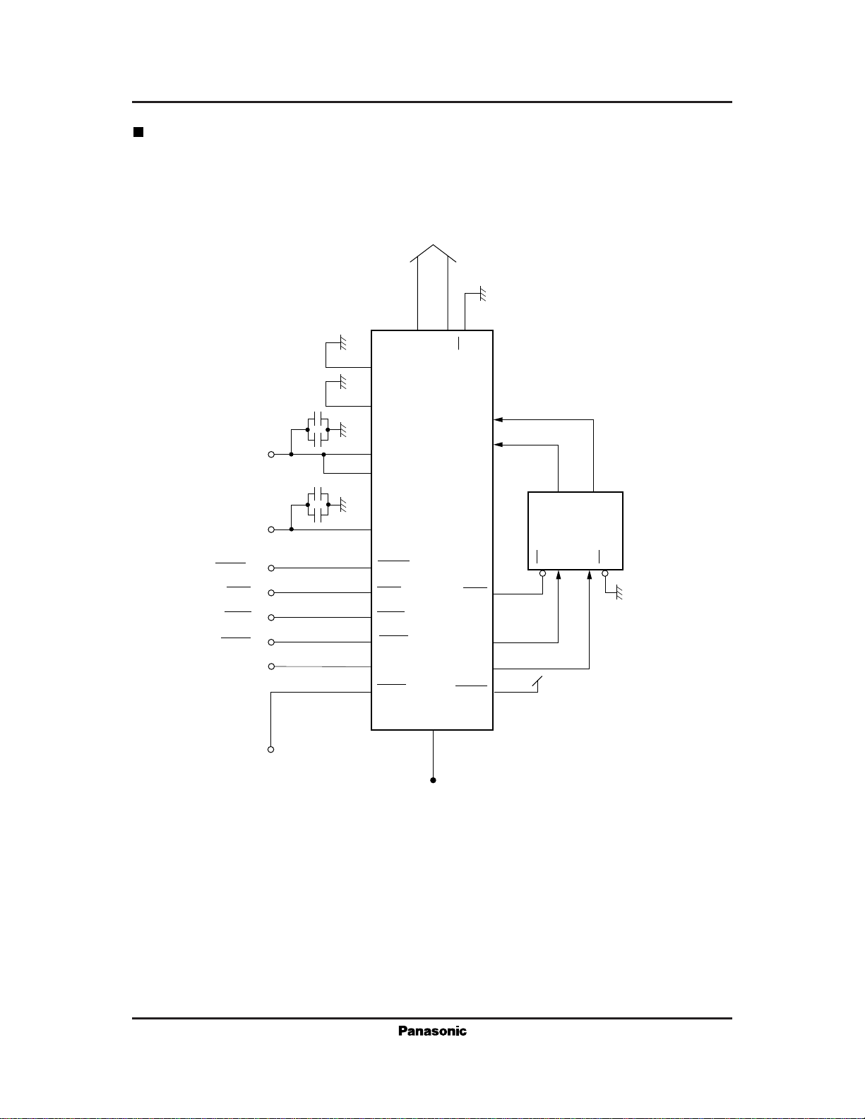
Application Circuit Example #2: Using ROM
DB0 to 5(O)
to
DB0
OE
DB5
V
SS
AV
DD
5V
AG AG AG AG
VREF
5V
ENBO(O)
INHI(I) INHI
ENBI(I) ENBI
CKSH(I)
ROS(H/L)
GND
V
DD
V
DD
VR
ENBO
CKSH
ROS
SHST
MN86157
MOE
A11
MODE
VIN
PIX
D6
D0
A0
to
to
D0
D6
ROM
2732
to
OECEA11
A0
to
Page 8
MN86157 For Communications Equipment
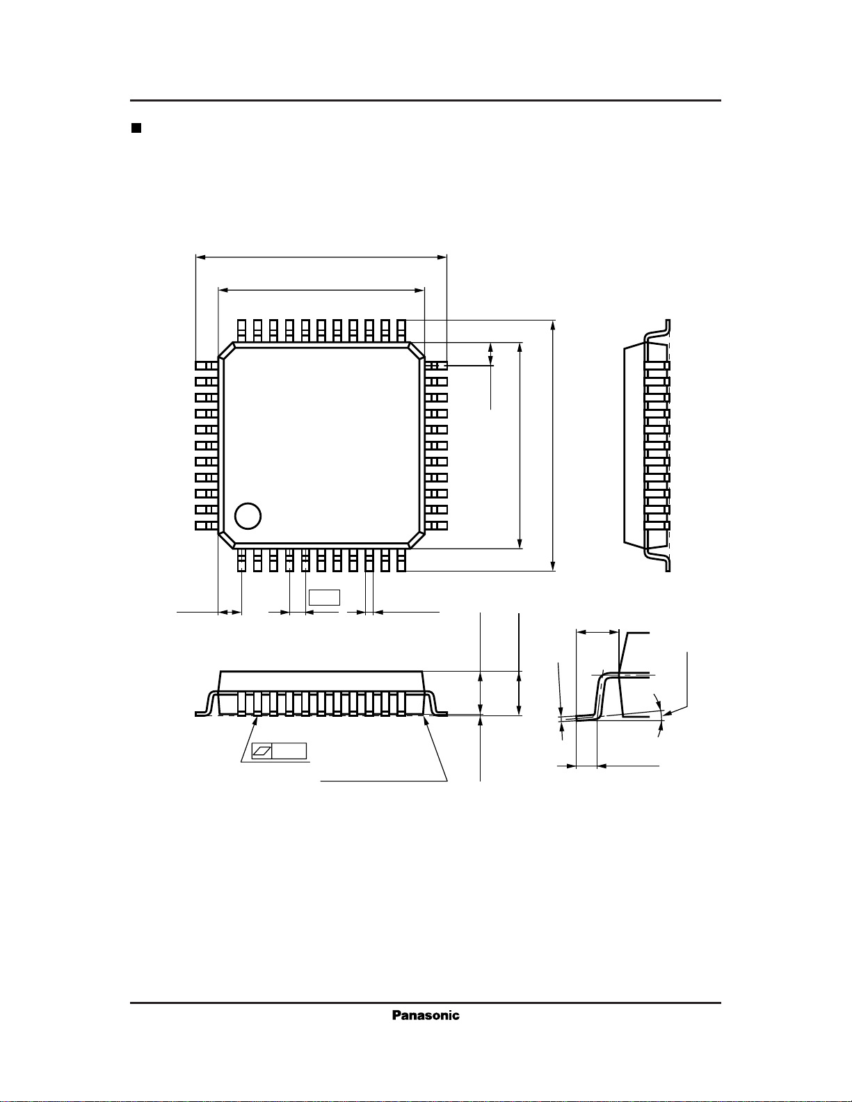
Packing Dimensions (Unit: mm)
QFP044-P-1010
12.30±0.40
10.00±0.20
34
44
(1.00)
33
23
22
(1.00)
10.00±0.20
12.30±0.40
12
111
0.80
0.35±0.10
2.00±0.20
2.10±0.30
+0.10
1.15±0.20
0.05
-
0.15
0 to 10°
0.10
SEATING PLANE
0.10±0.10
0.60
±0.20
 Loading...