

Page 1
A/D, D/C Converters for Image Signal Processing
MN657011H
Low Power 8-Bit, 3-Channel CMOS D/A Converter for Image Processing
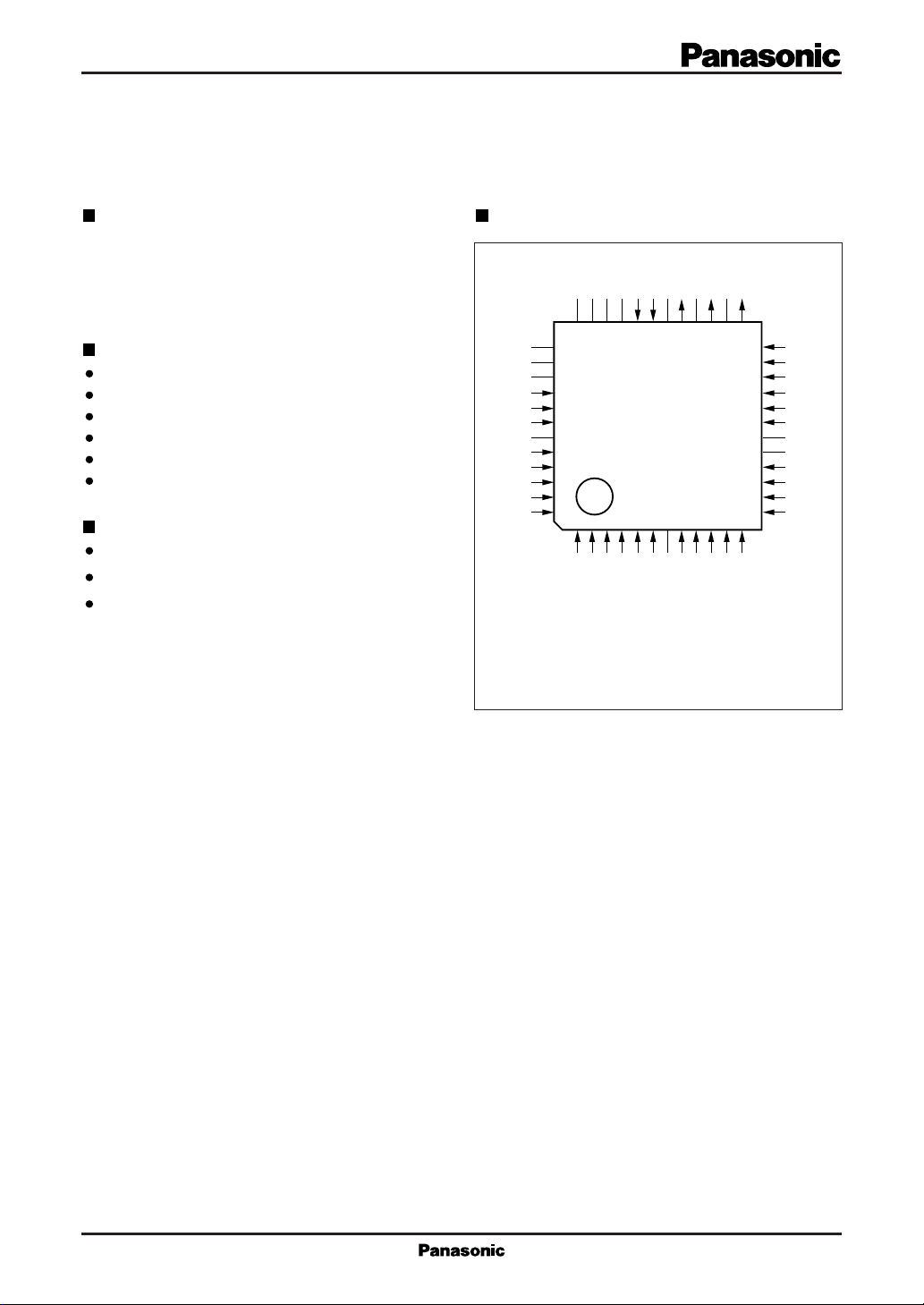
Pin Assignment Overview
The MN657011H is an 8-bit, 3-channel CMOS digitalto-analog converter with a maximum conversion rate of
20 MSPS.
It is a 3.5 volt version of the MN65701FHP.
Features
Maximum conversion rate: 20 MSPS (min.)
Linearity error: ±0.2 LSB (typ.)
Differential linearity error: ±0.2 LSB (typ.)
Power supply voltage: 3.5±0.1 V
Full scale current: 4 mA (typ.)
Power consumption: 84 mW (typ.) (f
=15 MHz)
CLK
Applications
Digital television
Digital video equipment
Digital image processing equipment
N.C.
N.C.
N.C.
NTCS
UVSEL
DV
N.C.
DV
DC8
DC7
DC6
DC5
N.C.
3635343332313029282726
37
38
39
40
41
42
SS
43
44
DD
45
46
47
48
1234567891011
DC4
SSAVSS
N.C.
N.C.
N.C.
AV
DC3
DC2
DC1
CLK
DV
(TOP VIEW)
DY8
IOUN.C.
DY7
DY6
OY
I
25
24
23
22
21
20
19
18
17
16
15
14
13
12
DY5
VIB
COMP
V
I
AV
AV
N.C.
N.C.
DY1
DY2
DY3
DY4
N.C.
IOVN.C.
SS
DD
N.C.
DV
REF
REF
DD
DD
QFH048-P-0707
1
Page 2
MN657011H A/D, D/C Converters for Image Signal Processing
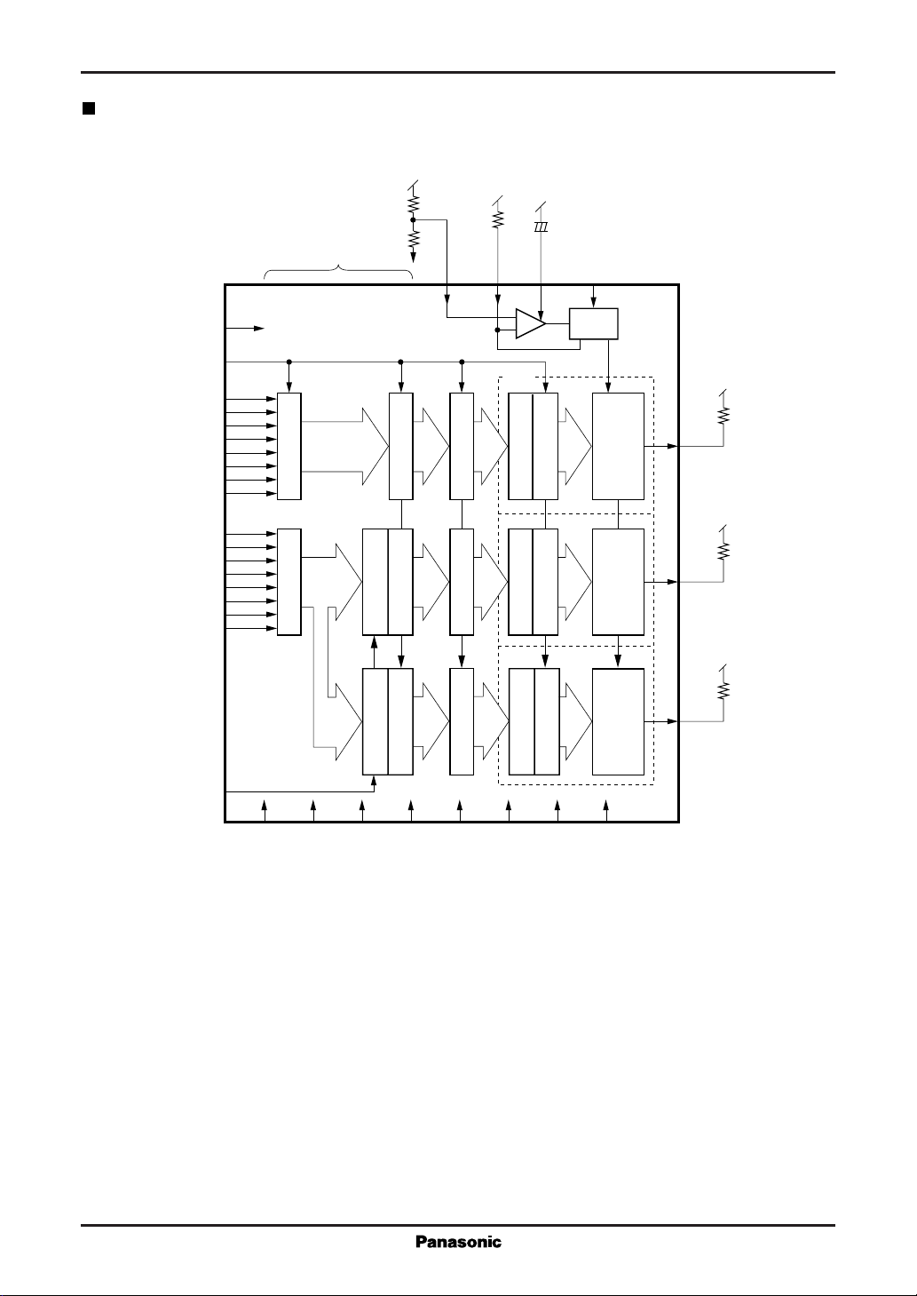
Block Diagram
NTSC
CLK
(MSB)DY1
DY2
DY3
DY4
DY5
DY6
DY7
(LSB)DY8
(MSB)DC1
DC2
DC3
DC4
DC5
DC6
DC7
(LSB)DC8
N.C.
N.C.
N.C.
N.C.
N.C.
N.C.
N.C.
UVSEL
40
5
16
15
14
13
12
11
10
9
4
3
2
1
48
47
46
45
33
34
35
36
37
38
39
41
7
LatchLatch
19
AVDDAV
N.C.
1716262830
Selector
Selector
20
31
DD
AVSSAV
43
LatchLatch
Latch
32
SS
R
REF
REF
V
22
Latch
LatchLatch
8
DVDDDV
+–
C
COMP
REF
I
21
23 COMP
+
–
VIB
24
Current
Source
DAC
R
OUT
OY
R
OUT
OU
R
OUT
OV
44
Decoder
Decoder
Decoder
DD
Latch
Latch
Latch
6
Current CellCurrent CellCurrent Cell
42
SS
I
25
I
27
I
29
DVSSDV
2
Page 3

A/D, D/C Converters for Image Signal Processing MN657011H
Pin Descriptions
Pin No. Symbol Function Description
1 DC4 C (chroma) digital input
2 DC3 C (chroma) digital input
3 DC2 C (chroma) digital input
4 DC1 C (chroma) digital input (MSB)
5 CLK Sampling clock
6DVSSGround for digital circuits
7 N.C. No connection
8DVDDPower supply for digital circuits
9 DY8 Y (luminance) digital input (LSB)
10 DY7 Y (luminance) digital input
11 DY6 Y (luminance) digital input
12 DY5 Y (luminance) digital input
13 DY4 Y (luminance) digital input
14 DY3 Y (luminance) digital input
15 DY2 Y (luminance) digital input
16 DY1 Y (luminance) digital input (MSB)
17 N.C. No connection
18 N.C. No connection
19 AV
20 AV
21 I
22 V
DD
DD
REF
REF
23 COMP Phase compensation
24 VIB Capacitor connection
25 I
OY
26 N.C. No connection
27 I
OU
28 N.C. No connection
29 I
OV
30 N.C. No connection
31 AV
32 AV
SS
SS
33 N.C. No connection
34 N.C. No connection
35 N.C. No connection
36 N.C. No connection
37 N.C. No connection
38 N.C. No connection
39 N.C. No connection
40 NTCS Format selection (two's complement/binary) for C (chroma) signal
41 UVSEL U/V signal discrimination for C (chroma) signal
42 DV
SS
Power supply for analog circuits
Power supply for analog circuits
Full scale adjustment resistor
Reference voltage input
Y signal analog current output
U signal analog current output
V signal analog current output
Ground for analog circuits
Ground for analog circuits
Ground for digital circuits
3
Page 4

MN657011H A/D, D/C Converters for Image Signal Processing
Pin Descriptions (continued)
Pin No. Symbol Function Description
43 N.C. No connection
44 DV
DD
45 DC8 C (chroma) digital input (LSB)
46 DC7 C (chroma) digital input
47 DC6 C (chroma) digital input
48 DC5 C (chroma) digital input
Absolute Maximum Ratings Ta=25˚C
Parameter Symbol Rating Unit
Power supply voltage for digital circuits DV
Power supply voltage for analog circuits AV
Input voltage V
Output voltage V
Operating ambient temperature T
Storage temperature T
Power supply for digital circuits
DD
DD
I
O
opr
stg
– 0.3 to +7.0 V
– 0.3 to +7.0 V
DV
AV
SS
SS
– 0.3 to DV
– 0.3 to AV
+0.3 V
DD
+0.3 V
DD
–20 to +70 ˚C
–55 to +125 ˚C
Recommended Operating Conditions V
=AVDD=DVDD=3.5V, VSS=AVSS=DVSS=0V, Ta=25˚C
DD
Parameter Symbol min typ max Unit
Power supply voltage V
Reference voltage V
Reference resistance R
External compensation capacitor C
Output load resistance R
Digital input "H" level V
voltage "L" level V
Clock "H" level pulse width t
"L" level pulse width t
Electrical Characteristics DV
DD
DD
REF
REF
COMP
OUT
IH
IL
WH
WL
=AVDD=3.5V, DVSS=AVSS=0V, Ta=25˚C
3.4 3.5 3.6 V
1.5 1.9 3.5 V
820 Ω
0.33 1.0 3.3 µF
200 Ω
VDD × 0.5 V
V
SS
DD
VDD × 0.16 V
15 ns
15 ns
V
Parameter Symbol Conditions min typ max Unit
Power supply voltage I
DD
VDD=3.5V, f
R
=200Ω, Output amplitude = 0.8V 24 40 mA
OUT
CLK
=15MHz
T=25˚C
Resolution RES 8 bit
Linearity error E
Differential linearity error E
Full scale current I
Setup time t
Hold time t
Settling time t
Maximum conversion speed F
C(max.)RREF
Analog output delay time t
L
D
FS
S
H
ST
d
VDD=3.5V, R
R
=820Ω±0.2 ±0.5 LSB
REF
V
=1.9V 4 mA
REF
=200Ω±0.2 ±0.5 LSB
OUT
10 ns
10 ns
VDD=3.5V, R
=820Ω V
=200Ω 30 50 ns
OUT
=1.9V 20 33 MSPS
REF
10 ns
4
Page 5

A/D, D/C Converters for Image Signal Processing MN657011H
Timing Chart
t
t
WH
WL
× 0.5
V
CLK
tSt
H
V
DD
DD
× 0.16
DY1 to DY8
DC1 to DC8
UVSEL
I
OY
I
OU
I
OV
Y-1
V-2
Y0 Y1 Y2 Y3 Y4 Y5
t
t
S
H
U0
V0 U2 V2 U4 V4
U-2 U-2 U0 U0 U2
V-2
Three clock cycles
V-2 V0 V0 V2
t
t
d
ST
td: Analog output delay time
t
: Settling time
ST
Y2Y1Y0Y-1Y-2
5
Page 6

MN657011H A/D, D/C Converters for Image Signal Processing
Package Dimensions (Unit:mm)
QFH048-P-0707
9.0
±0.2
±0.2
7.0
36 25
37
48
(0.75)
24
(0.75)
±0.2
±0.2
7.0
9.0
13
1
0.5
0.2
12
±0.1
(1.0)
0.05
-
+0.10
2.9 max.
0.15
0.5
±0.2
0 to 10°
0.1
SEATING PLANE
±0.2
2.5
±0.1
0.1
6
 Loading...