

Page 1
A/D, D/C Converters for Image Signal Processing
MN6556A, MN6556AS
Low Power 8-Bit CMOS D/A Converters for Image Processing
Overview
The MN6556A and MN6556AS are 8-bit CMOS digital-to-analog converters with a maximum conversion rate
of 20 MSPS.
They use both a matrix cell and weighted current technology to achieve a low power consumption of only 50
mW . Output has an amplitude of one volt abo ve the ground
level.
Features
Maximum conversion rate: 20 MSPS (min.)
Linearity error: ±0.3 LSB (typ.)
Differential linearity error: ±0.3 LSB (typ.)
Power supply voltage: 5.0±0.5 V
Power consumption: 50 mW (typ.)
Full scale current: 5 mA (typ.)
Applications
Digital television
Digital video equipment
Digital image processing equipment
Measuring instrument
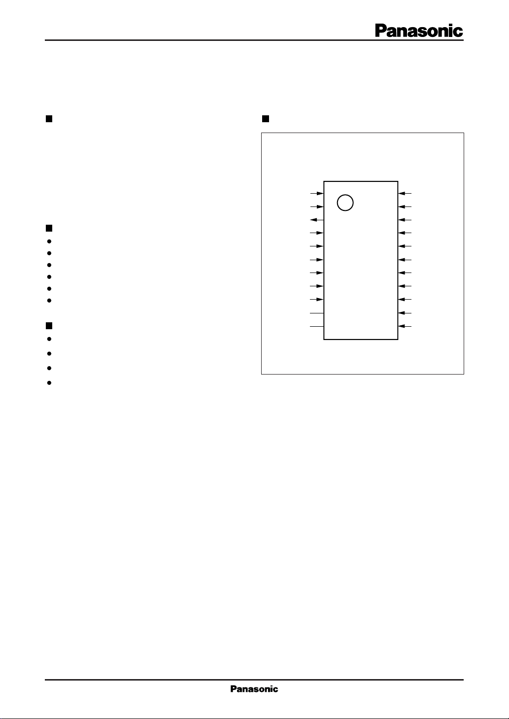
Pin Assignment
MN6556A : DIP022-P-0400
MN6556AS : SOP022-P-0375
AV
AV
VC
VIB
COMP
V
REF
I
REF
AV
N.C.
N.C.
DD
DD
1
2
3
I
O
4
5
6
7
8
9
SS
10
11
(TOP VIEW)
22
21
20
19
18
17
16
15
14
13
12
DV
DB8
DB7
DB6
DB5
DB4
DB3
DB2
DB1
CLK
DV
SS
DD
1
Page 2
MN6556A, MN6556AS A/D, D/C Converters for Image Signal Processing
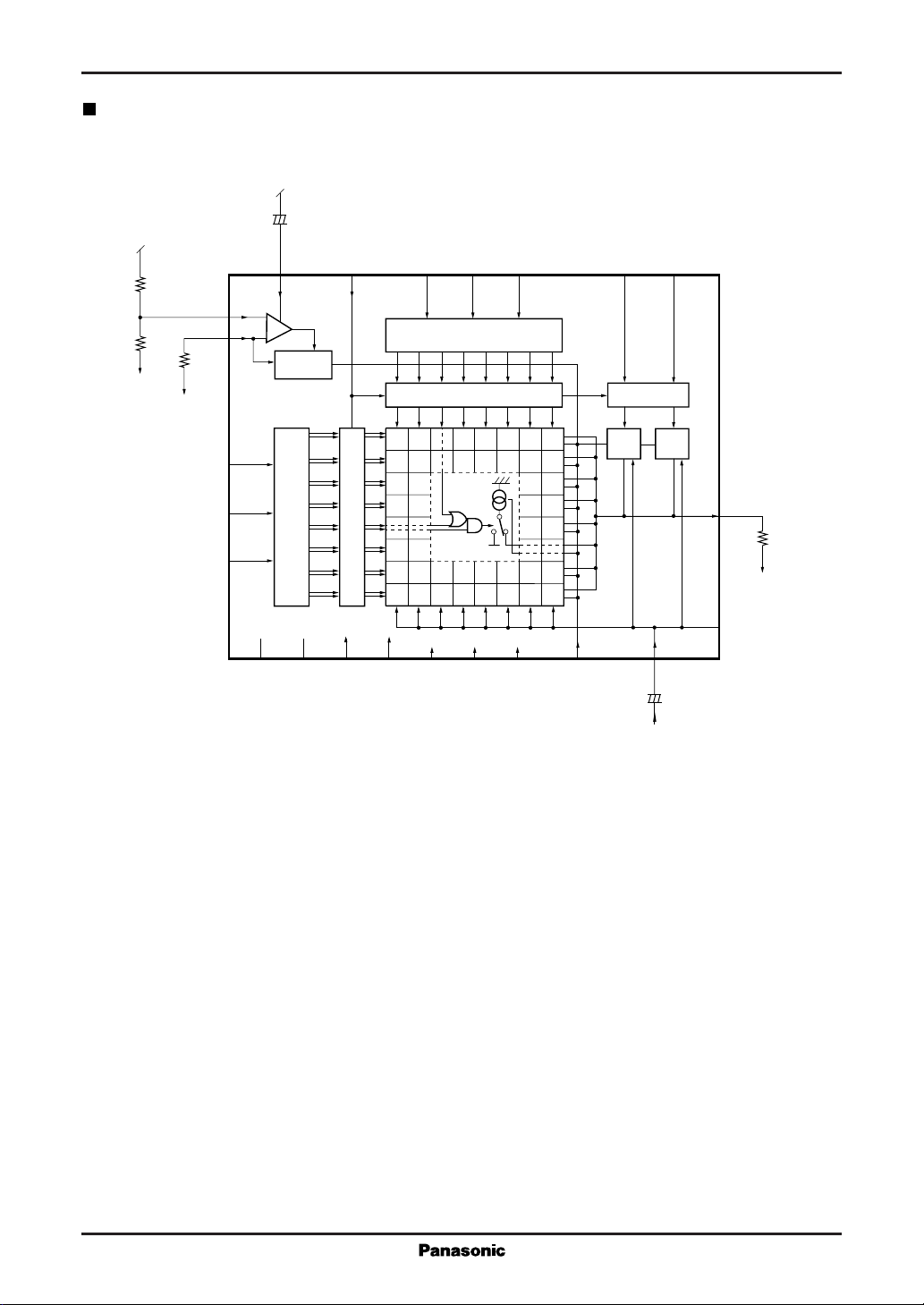
Block Diagram
+
–
DB4
DB5
V
I
R
DB3
REF
REF
REF
COMP
6
13
CLK
17
18
DB6
19
7
8
Current
Source
X-Decoder
Latch
16
20
1/2
DB7
Latch
1/4
21
DB8
(LSB)
DB2
DB1
(MSB)
15
N.C.
12
Latch
DD
DV
Matrix Current Cell
22
1
SS
DV
2
DD
AVDDAV
SS
AV
5
VIB
9
4
VC
+
–
10
Y-Decoder
11
14
N.C.
3
I
O
R
OUT
2
Page 3

A/D, D/C Converters for Image Signal Processing MN6556A, MN6556AS
Pin Descriptions
Pin No. Symbol Function Description
1AVDDPower supply for analog circuits
2AVDDPower supply for analog circuits
3IOAnalog current output
4 VC Capacitor connection
5 VIB Capacitor connection
6 COMP Phase compensation
7V
8I
REF
REF
9AVSSGround for analog circuits
10 N.C. No connection
11 N.C. No connection
12 DV
DD
13 CLK Sampling clock
14 DB1 Digital input (MSB)
15 DB2 Digital input
16 DB3 Digital input
17 DB4 Digital input
18 DB5 Digital input
19 DB6 Digital input
20 DB7 Digital input
21 DB8 Digital input (LSB)
22 DV
SS
Reference voltage input pin
Reference resistor
Ground for digital circuits
Power supply for digital circuits
Absolute Maximum Ratings Ta=25˚C
Parameter Symbol Rating Unit
Power supply voltage for digital circuits DV
Power supply voltage for analog circuits AV
Input voltage V
Output voltage V
Operating ambient temperature T
Storage temperature T
opr
stg
O
DD
DD
I
– 0.3 to +7.0 V
– 0.3 to +7.0 V
DVSS – 0.3 to DV
AVSS – 0.3 to AV
+0.3 V
DD
+0.3 V
DD
–20 to +70 ˚C
–55 to +125 ˚C
3
Page 4

MN6556A, MN6556AS A/D, D/C Converters for Image Signal Processing
Recommended Operating Conditions V
=AVDD=DVDD=5.0V, VSS=AVSS=DVSS=0V, Ta=25˚C
DD
Parameter Symbol min typ max Unit
Power supply voltage V
Reference voltage V
Reference resistance R
External compensation capacitor C
Output load resistance R
Digital input "H" level V
voltage "L" level V
Clock "H" level pulse width t
"L" level pulse width t
Electrical Characteristics DV
DD
DD
REF
REF
COMP
OUT
IH
IL
WH
WL
=AVDD=5.0V, DVSS=AVSS=0V, Ta=25˚C
4.5 5.0 5.5 V
1.8 V
1.5 kΩ
1 µF
200 Ω
2.4 V
V
SS
DD
0.8 V
20 ns
20 ns
V
Parameter Symbol Conditions min typ max Unit
Power supply voltage I
DD
10 20 mA
Resolution RES 8 bit
Linearity error E
Differential linearity error E
Full scale current I
Setup time t
Hold time t
Settling time t
Maximum conversion speed F
R
L
REF
V
D
REF
R
FS
ST
C(max.)VREF
REF
S
H
R
REF
=1.5kΩ, R
=200Ω±0.3 ±0.5 LSB
OUT
=1.8V ±0.3 ±0.5 LSB
=1.5kΩ, V
=1.8V 4.5 5.0 5.5 mA
REF
15 ns
15 ns
=1.5kΩ, R
=200Ω 50 ns
OUT
=1.8V 20 MSPS
4
Page 5

A/D, D/C Converters for Image Signal Processing MN6556A, MN6556AS
Timing Chart
CLK
Data
Analog Output
(Settling waveform)
t
WH
t
S
t
WL
t
H
Dn-1 Dn Dn+1
±1/2LSB
An
t
dtST
tdt
2.4V
0.8V
±1/2LSB
ST
5
Page 6
MN6556A, MN6556AS A/D, D/C Converters for Image Signal Processing
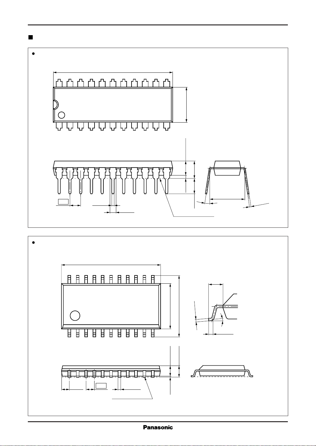
Package Dimensions (Unit:mm)
MN6556A DIP022-P-0400
27.7±0.4
22
12
8.6±0.2
1
2.54
0.5±0.1
MN6556AS SOP022-P-0375
15.30
22
111
1.2±0.1
±0.20
12
11
3.65±0.20
0.7min.
SEATING PLANE
±0.20
±0.30
7.20
5.3max.
3.3±0.3
0 to 15°
0.05
-
+0.10
0.15
10.16±0.20
1.10
±0.20
0.30min.
0 to 10°
0.25
+0.20
0.05
-
±0.20
2.00
2.40max. 9.40
(1.29) 0.40
1.27
SEATING PLANE
±0.10
±0.10
0.10
6
 Loading...