

Page 1
Power Amplifier for PHS
For the availability of this product, please contact the sales office.
Description
The CXG1010N is a power amplifier for PHS. This
IC is designed using the Sony’s GaAs J-FET process
and operates at a single power supply.
Features
• High output power 21.5 dBm
• Positive power supply drive VDD=3.4 V
• Low current consumption 200 mA
• High gain 40 dB Typ.
• Low distortion (ACP) –59 dBc Typ.
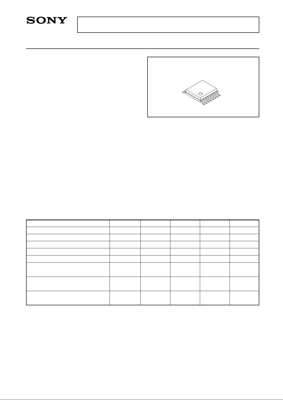
• Small mold package 16-pin SSOP
Structure
GaAs J-FET MMIC
CXG1010N
16 pin SSOP (Plastic)
Absolute Maximum Ratings (Ta=25 °C)
• Supply voltage VDD 6V
•Voltage between gate and source
Vgs0 1.5 V
• Drain current IDD 500 mA
• Power dissipation PD 3W
•Channel temperature Tch 175 °C
• Operating temperature Top –35 to +85 °C
• Storage temperature Tstg –65 to +150 °C
Electrical Characteristics
VDD=3.4 V, VCTL=2.0 V, f=1.90 GHz (Ta=25 °C)
Item Symbol Min. Typ. Max. Unit
∗1
Current consumption
∗1
Gate voltage adjustment value
Input VSWR
Output power (for –15.5 dBm input)
∗2
Power gain
∗2
Gain control
∗3
∗2
Average leak power level
(600 kHz±100 kHz)
∗
2
Average leak power level
(900 kHz±100 kHz)
∗1This value is adjusted by VGG1 and VGG2 set with Sony’s recommended current adjustment method when
21.5 dBm is output. In this time, the voltage ratio of VGG1 and VGG2 should match to the voltage ratio
generated by the resistance of the recommended gate bias circuit.
∗2When 21.5 dBm is output.
∗3GCTL=GP (VCTL 2.0 V)–GP (VCTL 0 V)
IDD 200 mA
VGG2 0 0.5 1.0 V
VSWRIN 1.5 2.0 —
POUT 21.5 dBm
GP 37 40 43 dB
GCTL 20 dB
PLEAK600 –59 –54 dBc
PLEAK900 –65 –59 dBc
Sony reserves the right to change products and specifications without prior notice. This information does not convey any license by
any implication or otherwise under any patents or other right. Application circuits shown, if any, are typical examples illustrating the
operation of the devices. Sony cannot assume responsibility for any problems arising out of the use of these circuits.
—1—
E95836-TE
Page 2
CXG1010N
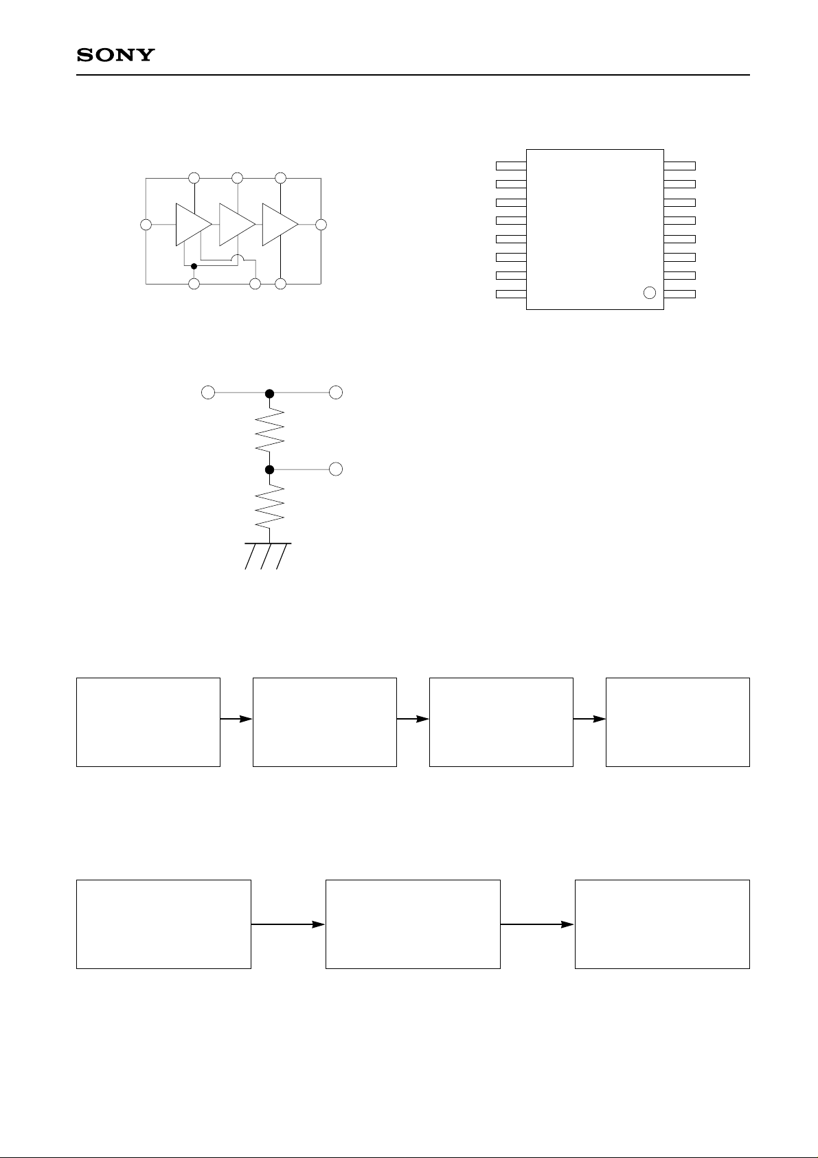
Block Diagram
VDD1VDD2VDD3
RFIN
VGG1VCTL VGG2
Gate adjustment pin
Gate adjustment pin
470Ω
680Ω
RF
OUT
V
V
GG2
GG1
Pin Configuration
GND
RF
OUT
GND
V
GG2
GND
VCTL
VGG1
GND
16
DD3
V
GND
DD2
V
GND
DD1
V
GND
IN
RF
GND
1
Recommended Current Adjustment Method
(1) VGG2/PIN separate adjustment
(VGG2 adjustment 1) (PIN adjustment 1) (VGG2 adjustment 2) (PIN adjustment 2)
When the RF input
(PIN) is off, the current
consumption (IDD) is
adjusted to 200 mA.
Variation of IDD and
POUT due to adjustment
The output power
(POUT) is adjusted
to 21.5 dBm.
IDD=200±20 mA
POUT=21.5 dBm
The current
consumption (IDD)
is finely adjusted to
200 mA.
IDD=200 mA
POUT=21.5±0.2 dBm
The output power
(POUT) is finely
adjusted to 21.5 dBm.
IDD=200±5 mA
POUT=21.5 dBm
(2) Simple adjustment
(IDD read) (VGG2 setting) (PIN adjustment)
When the RF input (PIN)
is off, the gate voltage
(VGG2) is set to 0.4 V
and it is read.
Variation of IDD and POUT
due to adjustment
The formula∗1where
VGG2=f (IDD: VGG2=0.4 V)
is used to set VGG2.
∗
1
e.g. VGG2=a-b x IDD IDD=200±5 mA
The output power (POUT)
is adjusted to 21.5 dBm.
POUT=21.5 dBm
—2—
Page 3

Current Consumption Variation with Recommended Current Adjustment Method
(For POUT=21.5 dBm output)
(1) Separate adjustment
V GG2/PIN separate adjustment method (Distribution of the
current consumption IDD after executing the PIN adjustment 1)
230
5/
180
00.8
V
GG2
(V)
I
(mA)
DD
CXG1010N
(2) Simple adjustment
GG2/PIN separate adjustment method (Distribution of the
V
(mA)
IDD
(mA)
current consumption IDD after executing the PIN adjustment 2)
220
5/
180
00.8
VGG2
Simple adjustment method (Distribution of the
current consumption IDD after executing the PIN adjustment)
GG2=a–b×IDD (Pin off/VGG2=0.4V): a=0.804, b=2.07
V
220
(V)
5/
DD
I
180
00.8
VGG2
(V )
—3—
Page 4

Recommended Evaluation Circuit
IN
RF
18n
10n
50mm
GND
1000p
470
680
VCTL
1µ
1µ
100Ω 6.8kΩ
VGG2
R
RV2
3.0V
V1
CXG1010N
Variable
resistor Rv
10kΩ (Max)
180Ω
GND GND
VDD
1µ
Recommended Gate Bias Circuit and
Circuit Characteristics
3.0V
R
RV2
V1
6.8kΩ
Variable
resistor Rv
10kΩ (Max)
180Ω
100Ω
VGG2
470Ω
V
(V)
GG2
0.5
ViaHole
RFOUT
Glass fabric-base epoxy board (0.2 mm thickness)
GND for the overall back side
VGG1
680Ω
0510
RV1 (kΩ)
Application circuits shown are typical examples illustrating the operation of the devices. Sony cannot assume responsibility for
any problems arising out of the use of these circuits or for any infringement of third party and other right due to same.
—4—
Page 5

Example of Representative Characteristics (Ta=25 °C)
Input/output characteristics (POUT/ACP)
VDD=3.4V, Vctl=2.0V,IDD=200mA@POUT=21.5dBm
25
23
21
19
CXG1010N
–40
21.5dBm
–45
17
15
13
-Output power (dBm)
OUT
11
P
9
7
5
–40 –35 –30 –25 –20 –15
GAIN, ACP vs. IDD
Freq=1.9GHz, VDD=3.4V, Vctl=2.0V, POUT constant
45
44
43
42
POUT=22dBm
41
40
POUT=21.5dBm
GAIN
POUT=21.5dBm
39
38
POUT=22dBm
37
36
GAIN-Gain (dB)
35
34
33
ACP
32
31
30
140 150 160 170 180 190 200 210 220 230 240 250 260
IDD-Current consumption (mA)
POUT
ACP
PIN-Input power (dBm)
Frequency=1.9 GHz, Vctl=2.0 V, PINVGG2 constant
(IDD=200mA@VDD=3.4V)
–48
24
–49
–50
–51
23
–52
–53
–54
22
–55
–56
–57
–58
–59
–60
21
-Output power (dBm)
OUT
P
20
–61
ACP-Leak power ratio of adjacent channel (dBc)
–62
–63
19
23452
POUT=22dBm
@VDD=3.4V
–50
–55
ACP-Leak power ratio of adjacent channel (dBc)
–60
POUT, ACP vs. VDD
POUT
POUT=21.5dBm
@VDD=3.4V
ACP
POUT=21.5dBm
@VDD=3.4V
DD-Drain voltage (V)
V
POUT=22dBm
@VDD=3.4V
–50
–51
–52
–53
–54
–55
–56
–57
–58
–59
–60
ACP-Leak power ratio of adjacent channel (dBc)
—5—
Page 6

Package Outline Unit : mm
CXG1010N
16PIN SSOP (PLASTIC)
∗5.0 ± 0.1
16
1
+ 0.1
0.22 – 0.05
NOTE: Dimension “∗” does not include mold protrusion.
9
∗4.4 ± 0.1
8
0.65 ± 0.12
0° to 10°
DETAIL A
0.1 ± 0.1
0.5 ± 0.2
A
+ 0.05
0.15 – 0.02
+ 0.2
1.25 – 0.1
6.4 ± 0.2
0.1
SONY CODE
EIAJ CODE
JEDEC CODE
SSOP-16P-L01
SSOP016-P-0044
PACKAGE STRUCTURE
PACKAGE MATERIAL
LEAD TREATMENT
LEAD MATERIAL
PACKAGE WEIGHT
EPOXY RESIN
SOLDER / PALLADIUM
COPPER / 42 ALLOY
0.1g
PLATING
—6—
 Loading...