

Page 1

CXD3029R
Description
The CXD3029R is a digital signal processor LSI for CD
players. This LSI incorporates a digital servo, high & bass
boost, shock-proof memory controller, 1-bit DAC and
analog low-pass filter.
Features
• All digital signal processing during playback is performed
with a single chip
• Highly integrated mounting possible due to a built-in RAM
Digital Signal Processor (DSP) Block
• Supports CAV (Constant Angular Velocity) playback
• Frame jitter free
• 0.5× to 4× speed continuous playback possible
• Allows relative rotational velocity readout
• Wide capture range playback mode
• Spindle rotational velocity following method
• Supports 1× to 4× speed playback
• Supports variable pitch playback
• The bit clock, which strobes the EFM signal, is generated
by the digital PLL.
• EFM data demodulation
• Enhanced EFM frame sync signal protection
• Refined super strategy-based powerful error correction
C1: double correction, C2: quadruple correction
Supported during 4× speed playback
• Noise reduction during track jumps
• Auto zero-cross mute
• Subcode demodulation and subcode-Q data error
detection
• Digital spindle servo
• 16-bit traverse counter
• Asymmetry correction circuit
• CPU interface on serial bus
• Error correction monitor signal, etc. output from a new
CPU interface
• Servo auto sequencer
• Fine search performs track jumps with high accuracy
• Digital audio interface outputs
• Digital level meter, peak meter
• Bilingual compatible
• VCO control mode
• CD TEXT data demodulation
• Digital Out can be generated from the audio serial input.
(also supported after shock-proof and digital bass boost
processing, subcode-Q addition function)
Digital Servo (DSSP) Block
• Microcomputer software-based flexible servo control
• Offset cancel function for servo error signal
• Auto gain control function for servo loop
• E:F balance, focus bias adjustment functions
• Surf jump function supporting micro two-axis
• Tracking filter: 6 stages
Focus filter: 5 stages
Shock-proof Memory Controller Block
• Supports an external 4M-bit/16M-bit DRAM
• Time axis-based data linking
• ADPCM compression method (uncompressed/4 bits/
6 bits/8 bits)
Digital Filter, DAC and Analog Low-pass Filter Blocks
• Digital dynamic bass boost and high boost
Bass Boost:4th-order IIR 24dB/Oct
+10dB/+14dB/+18dB/+22dB
High Boost: Second-order IIR 12dB/Oct
+4dB/+6dB/+8dB/+10dB
• Independent turnover frequency selection possible
Bass Boost: 125Hz/160Hz/200Hz
High Boost: 5kHz/7kHz
• Digital dynamics (compressor)
Volume increased by +5dB at low level
• 8× oversampling digital filter
(attenuation: 61dB, ripple within band: ±0.0075dB)
• Digital signal output possible after boost
• Serial data format selectable from (output) 20 bits/
18 bits/16 bits (rearward truncation, MSB first)
• Digital attenuation: –∞, –60 to +6dB, 2048 steps (linear)
• Soft mute
• Digital de-emphasis
• High-cut filter
Applications
CD players
Structure
Silicon gate CMOS IC
Absolute Maximum Ratings
• Supply voltage V
DD, AVDD –0.3 to +4.6 V
• Input voltage V
I –0.3 to +4.6 V
(V
SS – 0.3V to VDD + 0.3V)
• Output voltage V
O –0.3 to +4.6 V
•
Storage temperature
Tstg –40 to +125 °C
• Supply voltage difference
AV
SS – VSS –0.3 to +0.3 V
AV
DD – VDD –0.3 to +0.3V(AVDD < 2.2V)
AV
DD – VDD –0.3 to +1.4V(AVDD = 2.2 to 3.6V)
Recommended Operating Conditions
• Supply voltage V
DD , AVDD0, 3 2.2 to 3.6 V
AV
DD1, 2, DVDD VDD to 3.6 V
•
Operating temperature
Topr –20 to +75 °C
I/O Pin Capacitance
• Input capacitance C
I 12 (max.) pF
• Output capacitance C
O 12 (max.) pF
Note) Measurement conditions V
DD = VI = 0V
f
M = 1MHz
– 1 –
E01429-PS
Sony reserves the right to change products and specifications without prior notice. This information does not convey any license by
any implication or otherwise under any patents or other right. Application circuits shown, if any, are typical examples illustrating the
operation of the devices. Sony cannot assume responsibility for any problems arising out of the use of these circuits.
120 pin LQFP (Plastic)
CD Digital Signal Processor with Built-in Digital Servo +
Shock-proof Memory Controller + Digital High & Bass Boost
Page 2
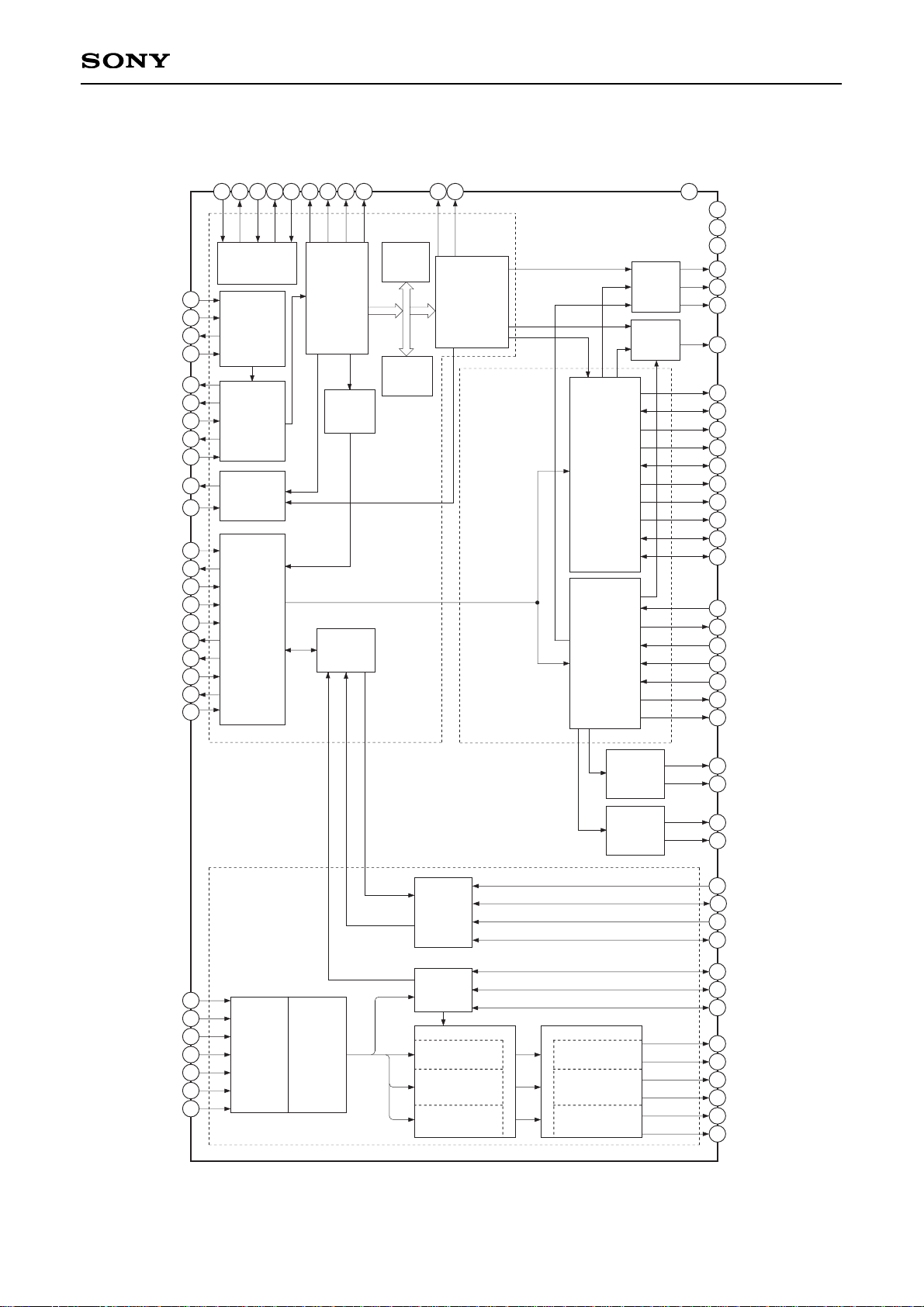
– 2 –
CXD3029R
A0 to A11
D0 to D3
XEMP
XWIH
XQOK
BCK
LRCK
DOUT
PCMD
XRST
TEST
TES1
D/A
Interface
EFM
demodulator
Error
Corrector
32K
RAM
Sub Code
Processor
Clock
Generator
Asymmetry
Corrector
Digital
PLL
CPU
Interface
C2PO
WFCK
EMPH
GFS
XUGF
XTAI
RFAC
ASYI
ASYO
BIAS
FILO
FILI
PCO
CLTV
MDP
PWMI
SENS
DATA
XLAT
CLOK
SCOR
SBSO
EXCK
WDCK
XTAO
VPCO
VCTL
XPCK
SQSO
SQCK
Digital
CLV
SERVO
Interface
ATSK
SCLK
SSTP
MIRR
DFCT
FOK
MIRR
DFCT
FOK
SERVO DSP
FOCUS SERVO
TRACKING
SERVO
SLED SERVO
PWM GENERATOR
FOCUS PWM
GENERATOR
TRACKING PWM
GENERATOR
SLED PWM
GENERATOR
FFDR
FRDR
TFDR
TRDR
SFDR
SRDR
RFDC
CE
TE
SE
FE
VC
IGEN
OPAmp
Analog SW
A/D
Converter
COUT
XRAS
XWE
XCAS
XWRE
XRDE
Selecter
Digital
OUT
XTSL
Servo
Auto
Sequencer
XSOE
SYSM
LRMU
LRCKI
BCKI
PCMDI
LPF
AOUT1
VREFL
LPF
AOUT2
VREFR
DAC
HPL
HPR
Signal
Processor
Block
Servo Block
Memory Controller,
Bass Boost Block
Shock-proof
Memory
Controller +
Compression/
Expansion
TEST1 to 4
Block Diagram
Page 3
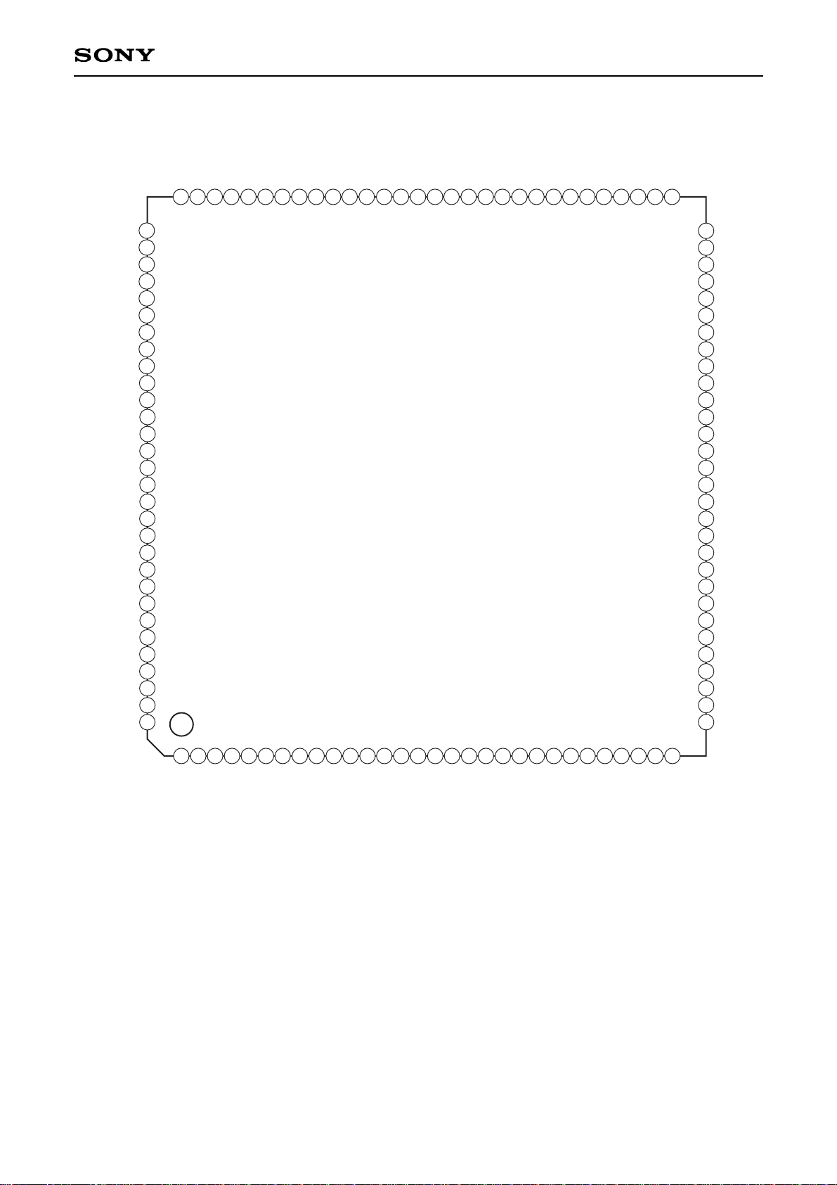
– 3 –
CXD3029R
Pin Configuration
36
35
34
31
32
33
2
3
4
5
6
7
8
9
10
11
12
13
14
15
16
17
18
19
20
21
22
23
24
25
26
27
28
29
30
1
40
39
38
37
41
42
43
44
45
46
47
48
49
50
51
52
53
54
55
56
57
58
59
60
70
69
68
67
63
64
65
66
61
62
71
72
97
96
95
94
91
92
93
99
98
73
74
81
82
83
84
75
76
77
78
88
87
86
85
79
80
89
90
TE
CE
RFAC
AV
DD
3
BIAS
ASYI
AV
SS
3
VPCO
VCTL
CLTV
FILO
FILI
PCO
V
DD
1
GFS
C2PO
COUT
MIRR
FOK
DFCT
ATSK
DOUT
AV
DD
0
ASYO
XUGF
LRMU
XRAS
XWE
D1
TEST1
TEST2
XCAS
WFCK
A9
A8
A7
DV
SS
A6
A5
A4
XRDE
V
DD
0
CLOK
DATA
SENS
XLAT
XSOE
SYSM
WDCK
SCOR
XRST
XQOK
D3
D2
D0
PWMI
HPL
HV
SS
XTSL
EXCK
SBSO
XWIH
XEMP
SCLK
SQCK
V
SS0
R4M
XWRE
VREFR
AV
SS2
AV
SS1
VREFL
AOUT1
AV
DD1
XV
SS
XTAO
XTAI
XV
DD
HVDD
HPR
TES1
AV
DD2
AOUT2
SQSO
TEST
V
SS1
XPCK
AV
SS
0
IGEN
RFDC
PCMD
PCMDI
BCK
BCKI
DV
DD
A3
A2
A0
A10
A11
TEST3
TEST4
FFDR
TRDR
TFDR
SRDR
SFDR
SSTP
MDS
MDP
C176
V
DD2
LRCKI
VC
V
SS2
FRDR
A1
FE
SE
LRCK
100
101
102
103
104
105
106
107
108
109
110
111
112
113
114
115
116
117
118
119
120
Page 4
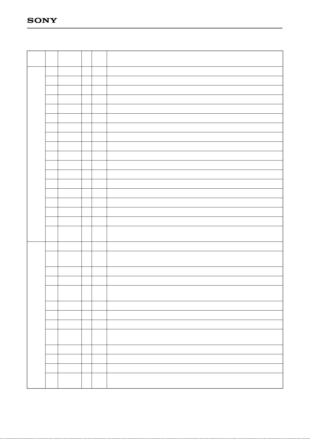
– 4 –
CXD3029R
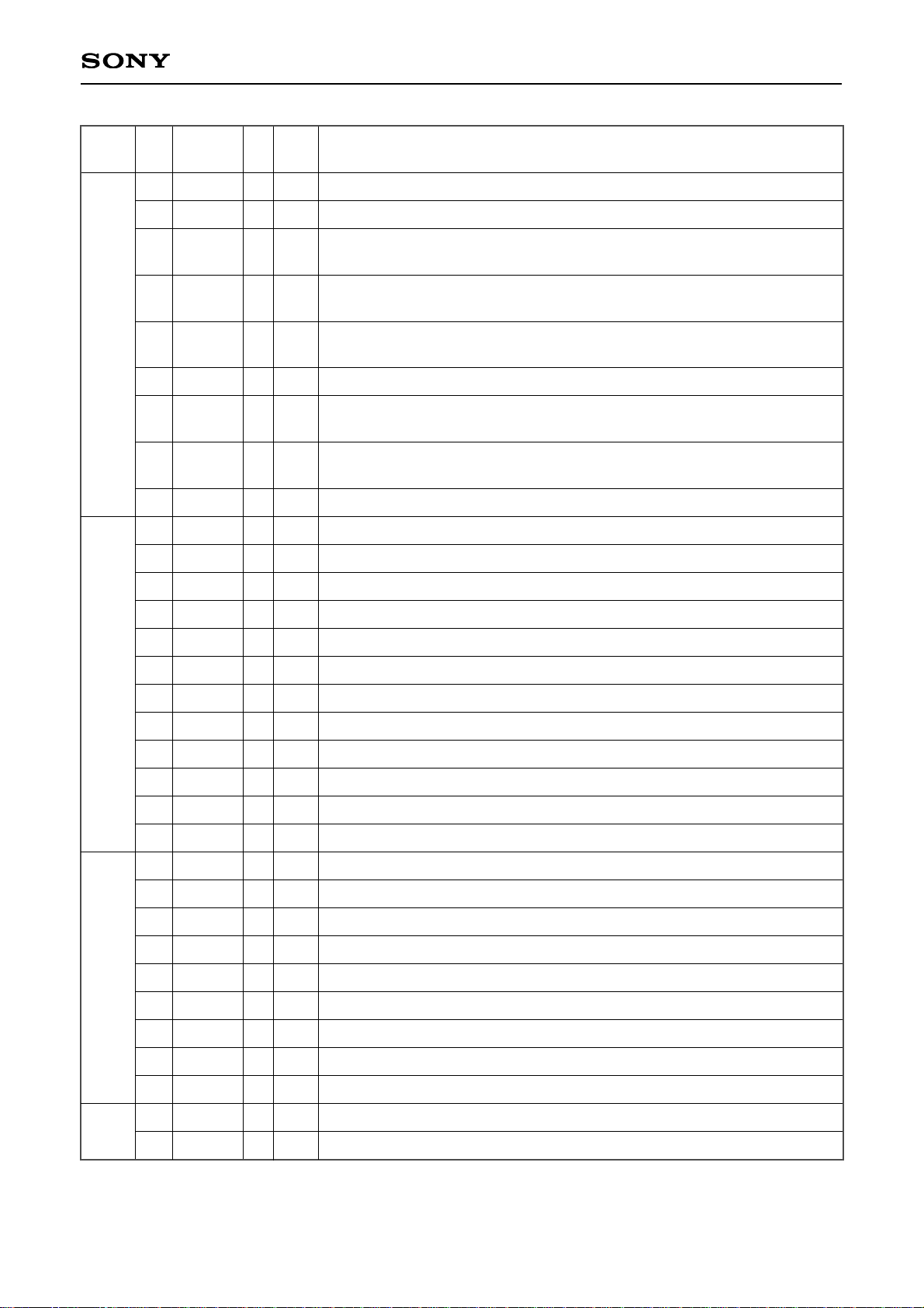
Pin Description
Pin
No.
1
2
3
4
5
6
7
8
9
10
11
12
13
14
15
16
17
18
19
20
21
22
23
24
25
26
27
28
29
30
31
Power
supply
2-3V
I/F
Digital
O
O
I/O
I/O
I/O
I/O
O
O
O
O
O
O
O
—
O
O
O
I/O
—
I
I
O
I
I
I
O
O
I
I
I/O
I/O
1, 0
1, 0
1, 0
1, 0
1, 0
1, 0
1, 0
1, 0
1, 0
1, 0
1, 0
—
1, 0
1, 0
1, 0
1, 0
—
1, Z, 0
1, 0
1, 0
1, 0
1, 0
DRAM row address strobe signal.
DRAM data input enable signal.
DRAM data bus 1.
DRAM data bus 0.
DRAM data bus 3.
DRAM data bus 2.
Test pin. Do not connect.
Test pin. Do not connect.
DRAM column address strobe signal.
WFCK output. XOE is output by switching with the command.
DRAM address 9.
DRAM address 8.
DRAM address 7.
DRAM interface GND.
DRAM address 6.
DRAM address 5.
DRAM address 4.
DRAM readout enable signal input. XRDE monitor is output by switching
with the command.
Digital power supply.
Serial data transfer clock input from CPU. SQSO and SENS readout
clocks are output by switching with the command.
Serial data input from CPU.
SENS output to CPU. SQSO data is output by switching with the command.
Latch input from CPU. The serial data is latched at the falling edge. XLAT
which is low for 6µs or more is enabled.
CPU serial data output enable signal.
Mute input. Muted when high.
Word clock output f = 2Fs. GRSCOR is output by switching with the command.
High output when the subcode sync is detected. SCOR, which is
interpolated in the IC, is output by switching with the command.
System reset. Reset when low.
Spindle motor external control input.
Subcode Q OK input. XQOK monitor is output by switching with the command.
DRAM write enable signal input. XWRE monitor is output by switching with
the command.
XRAS
XWE
D1
D0
D3
D2
TEST1
TEST2
XCAS
WFCK
A9
A8
A7
DV
SS
A6
A5
A4
XRDE
VDD0
CLOK
DATA
SENS
XLAT
XSOE
SYSM
WDCK
SCOR
XRST
PWMI
XQOK
XWRE
Symbol I/O Value
Description
Page 5
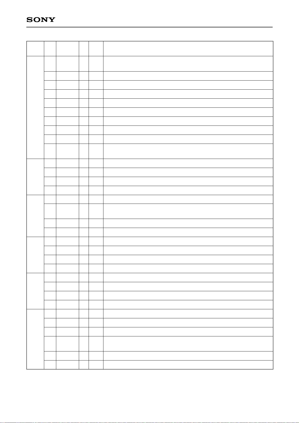
– 5 –
CXD3029R
Pin
No.
32
33
34
35
36
37
38
39
40
41
42
43
44
45
46
47
48
49
50
51
52
53
54
55
56
57
58
59
60
61
62
63
Power
supply
Digital
H/P
X'tal
Lch
Rch
Digital
O
—
I
I
O
O
O
O
I
I
—
O
O
—
I
O
—
O
O
—
—
O
O
—
I
I
—
O
O
I/O
1, 0
—
1, 0
1, 0
1, 0
1, 0
—
1, 0
1, 0
—
—
Analog
Analog
—
—
Analog
Analog
—
—
1, 0
1, 0
1, 0
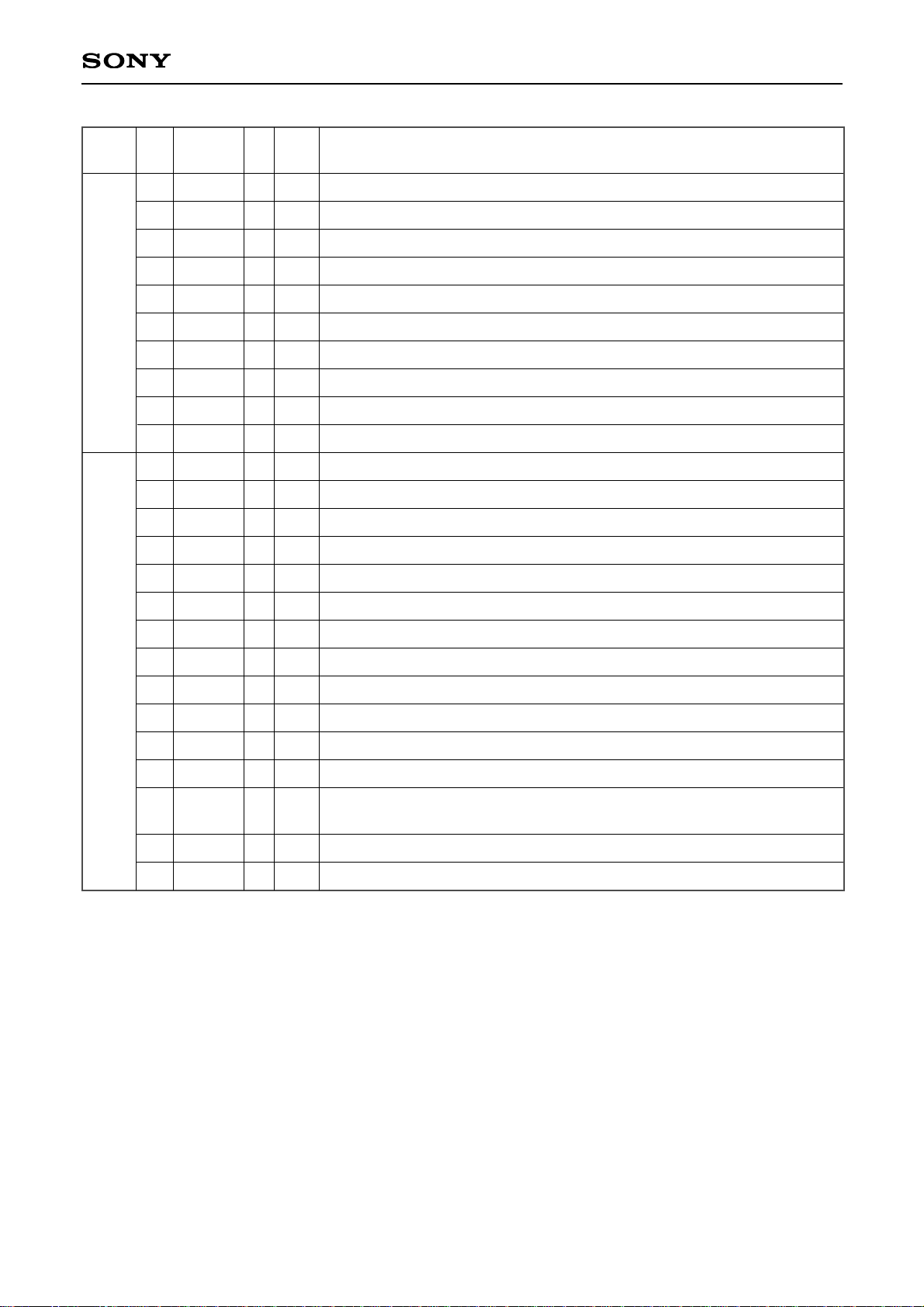
Microcomputer clock output. R8M and C4M are output by switching with
the command.
Digital GND.
SQSO readout clock input.
SENS serial data readout clock input.
Subcode Q 80-bit and PCM peak and level data output. CD TEXT data output.
DRAM readout prohibited signal.
Write to DRAM prohibited signal.
Subcode P to W serial output.
SBSO readout clock input.
Crystal selection input. Low when the crystal is 16.9344 MHz; high when
the crystal is 33.8688MHz.
Headphone GND.
Lch headphone PDM output.
Rch headphone PDM output.
Headphone power supply.
Master clock power supply.
Crystal oscillation circuit input. The master clock is externally input from
this pin.
Crystal oscillation circuit output.
Master clock GND.
Analog power supply.
Lch analog output.
Lch reference voltage.
Analog GND.
Analog GND.
Rch reference voltage.
Rch analog output.
Analog power supply.
Test pin. Normally GND.
Test pin. Normally GND.
Digital GND.
OR signal output of Lch, Rch “0” detection flag (AND output) and SYSM.
Only "0" detection flag is output by switching with the command.
Digital Out output.
Anti-shock input/output.
R4M
VSS0
SQCK
SCLK
SQSO
XEMP
XWIH
SBSO
EXCK
XTSL
HVSS
HPL
HPR
HVDD
XVDD
XTAI
XTAO
XVSS
AVDD1
AOUT1
VREFL
AVSS1
AVSS2
VREFR
AOUT2
AVDD2
TES1
TEST
VSS1
LRMU
DOUT
ATSK
Symbol I/O Value
Description
Page 6
– 6 –
CXD3029R
Pin
No.
64
65
66
67
68
69
70
71
72
73
74
75
76
77
78
79
80
81
82
83
84
85
86
87
88
89
90
91
92
93
94
95
Power
supply
Digital
ASYM
A/D
Digital
I/O
I/O
I/O
I/O
O
O
O
O
—
O
I
O
I
I
O
—
O
O
I
—
I
—
I
—
I
I
I
I
I
I
—
O
1, 0
1, 0
1, 0
1, 0
1, 0
1, 0
1, 0
1, 0
—
1, Z, 0
Analog
1, Z, 0
—
1, 0
—
—
—
—
1, 0
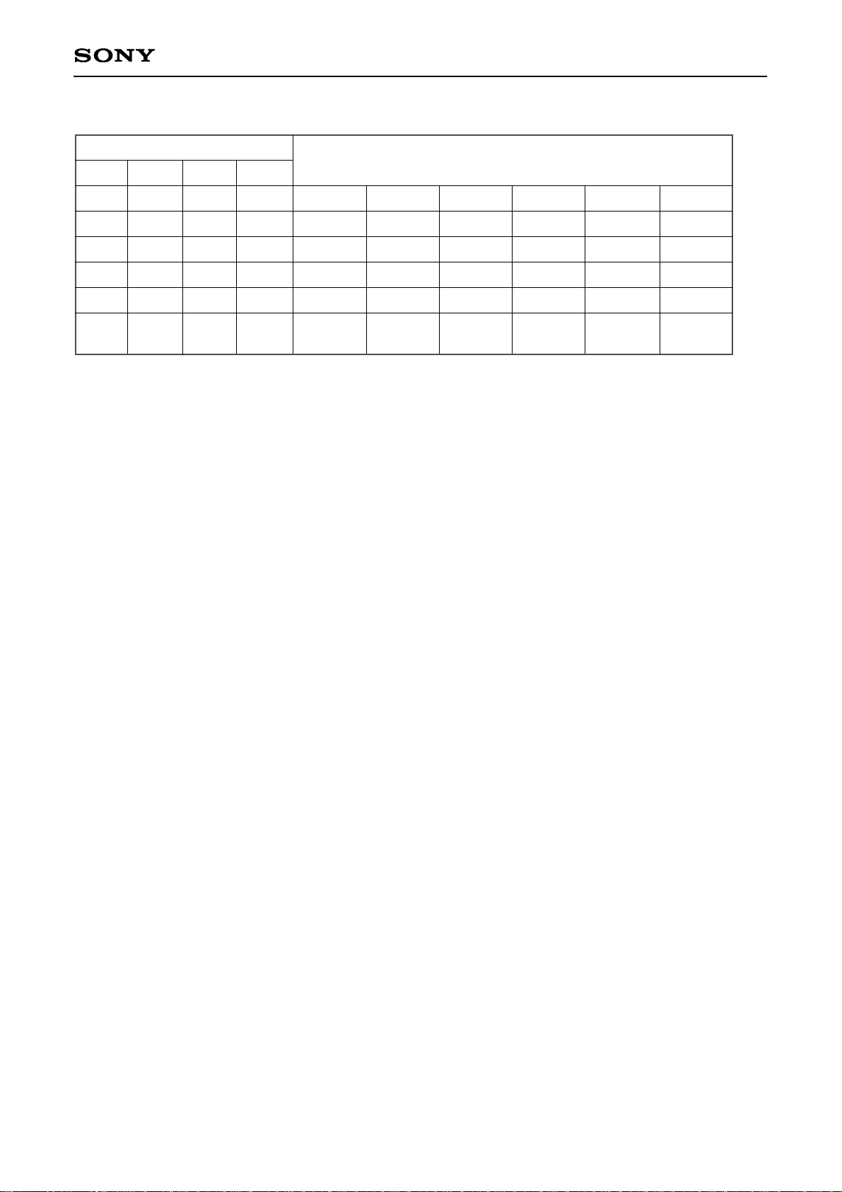
Defect signal input/output.
Focus OK signal input/output.
Mirror signal input/output. SCOR Window is output by switching with the
command.
Track number count signal input/output. SCOR is output by switching with
the command.
C2PO output. MNT3 and GTOP are output by switching with the
command.
GFS output. MNT2 and XROF are output by switching with the command.
XUGF output. MNT0, RFCK, C4M and QRCVD are output by switching
with the command.
XPCK output. MNT1, FSTO and GTOP are output by switching with the
command.
Digital power supply.
Master PLL charge pump output.
Master PLL filter input.
Master PLL (slave = digital PLL) filter output.
Multiplier VCO1 control voltage input.
Wide-band EFM PLL VCO2 control voltage input.
Wide-band EFM PLL charge pump output.
Analog GND.
EFM full-swing output (low = Vss, high = V
DD).
Asymmetry comparator voltage input.
Asymmetry circuit constant current input.
Analog power supply.
EFM signal input.
Analog power supply.
Operational amplifier constant current input.
Analog GND.
RF signal input.
Center servo analog input or E input.
Tracking error signal input or F input.
Sled error signal input or B input.
Focus error signal input or A input.
Center voltage input.
Digital GND.
Focus drive output.
DFCT
FOK
MIRR
COUT
C2PO
GFS
XUGF
XPCK
V
DD1
PCO
FILI
FILO
CLTV
VCTL
VPCO
AVSS3
ASYO
ASYI
BIAS
AVDD3
RFAC
AVDD0
IGEN
AVSS0
RFDC
CE
TE
SE
FE
VC
VSS2
FRDR
Symbol I/O Value
Description
Page 7
– 7 –
CXD3029R
Notes) • PCMD is a MSB first, two's complement output.
• GTOP is used to monitor the frame sync protection status. (High: sync protection window released.)
• XUGF is the frame sync obtained from the EFM signal, and is negative pulse. It is the signal before
sync protection.
• XPCK is the inverse of the EFM PLL clock. The PLL is designed so that the falling edge and the EFM
signal transition point coincide.
• The GFS signal goes high when the frame sync and the insertion protection timing match.
• RFCK is derived from the crystal accuracy, and has a cycle of 136µs.
• C2PO represents the data error status.
• XROF is generated when the 32K RAM exceeds the ±28 frame jitter margin.
• C4M is a 4.2336MHz output that changes in CAV-W mode and variable pitch mode.
• R8M is the 8.4672MHz output.
• FSTO is the 2/3 frequency-division output of the XTAI pin.
• SOUT is the serial data output inside the servo block.
• SOCK is the serial data readout clock output inside the servo block.
• XOLT is the serial data latch output inside the servo block.
Pin
No.
96
97
98
99
100
101
102
103
104
105
106
107
108
109
110
111
112
113
114
115
116
117
118
119
120
Power
supply
2-3V
I/F
O
O
O
O
O
I
O
O
O
—
O
I
O
I
O
I
—
O
O
O
O
O
I/O
O
O
1, 0
1, 0
1, 0
1, 0
1, 0
1, Z, 0
1, Z, 0
1, 0
—
1, 0
1, 0
1, 0
—
1, 0
1, 0
1, 0
1, 0
1, 0
1, 0
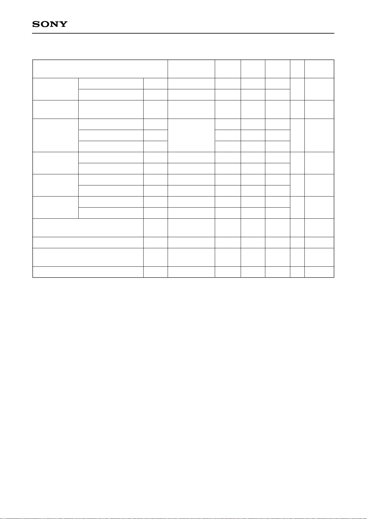
Focus drive output.
Tracking drive output.
Tracking drive output.
Sled drive output.
Sled drive output.
Disc innermost detection signal input.
Spindle drive output.
Spindle motor servo control output.
176.4kHz output. 88.2kHz for quasi-double speed setting.
Digital power supply.
D/A interface. LR clock output f = Fs.
D/A interface. LR clock input.
D/A interface. Serial data output. (two’s complement, MSB first)
D/A interface. Serial data input. (two’s complement, MSB first)
D/A interface. Bit clock output.
D/A interface. Bit clock input.
DRAM interface power supply.
DRAM address 3.
DRAM address 2.
DRAM address 1.
DRAM address 0.
DRAM address 10.
DRAM address 11. Write prohibition factor is input by switching with the
command.
Test pin. Do not connect.
Test pin. Do not connect.
FFDR
TRDR
TFDR
SRDR
SFDR
SSTP
MDS
MDP
C176
VDD2
LRCK
LRCKI
PCMD
PCMDI
BCK
BCKI
DVDD
A3
A2
A1
A0
A10
A11
TEST3
TEST4
Symbol I/O Value
Description
Digital
Page 8
– 8 –
CXD3029R
Monitor Pin Output Combinations
Command bit
Output data
SRO1
MTSL1
MTSL0
XUGF
XPCK
GFS
C2PO
MNT0
MNT1
MNT2
MNT3
RFCK
XPCK
XROF
GTOP
0
0
0
0
1
—
MONSEL
0
0
0
0
0
1
0
0
1
1
0
—
0
1
0
1
0
—
C4M
FSTO
GFS
C2PO
SOUT
SOCK
XOLT
C2PO
COUT
COUT
COUT
COUT
COUT
MIRR
MIRR
MIRR
MIRR
MIRR
QRCVD
GTOP
GFS
C2PO SCOR
SCOR
WINDOW
Page 9

– 9 –
CXD3029R
Electrical Characteristics
1. DC Characteristics (VDD1 = 3.3 ± 0.3V, VDD2 (logic) = 2.2 ± 0.2V, DVSS = VSS = 0V, Topr = –20 to +75°C)
Item
Input voltage
(1)
Input voltage
(2)
Input voltage
(3)
Input leak current (1)
∗
13
,
∗15
∗
14
∗12, ∗13
∗13
∗15
Schmitt input
I
OH = –4mA
IOL = 4mA
VIN = 0 to VDD
VIN = 0 to VDD
High level input voltage
Low level input voltage
High level input voltage
Low level input voltage
Hysteresis
High level output voltage
Low level output voltage
VIH
VIL
Vt+
Vt–
Vt+–
VOH
VOL
ILI (1)
ILI (2)
0.7VDD1
0.7VDD1
VDD1 – 0.4
0
–10
–40
0.2V
DD
1
0.2VDD1
VDD1
0.4
10
40
V
V
V
µA
µA
Conditions Min.
Typ.
Max.
Unit
Applicable
pins
Input leak current (2)
0.5
Input voltage
(1)
Input voltage
(2)
Input voltage
(3)
Output voltage
(1)
Output voltage
(2)
Output voltage
(3)
∗
1, ∗2,
∗
3, ∗4
∗
6, ∗7
∗
5
∗
2, ∗8,
∗
10, ∗15
Input leak current (1)
Input leak current (2)
Input leak current (3)
Tri-state output leak current
∗
1, ∗3,
∗
5, ∗6
∗
2, ∗4
V
V
V
V
∗
9
V
∗
11
V
µA
µA
∗
10
µA
∗
7
µA
Schmitt input
Analog input
I
OH = –4mA
IOL = 4mA
IOH = –1mA
IOL = 1mA
IOH = –0.28mA
IOL = 0.36mA
VIN = 0 to VDD
V
IN = 0 to VDD
V
IN = 0.25VDD
to 0.75V
DD
V
O = 0 to 3.6V
High level input voltage
Low level input voltage
Input voltage
High level input voltage
Low level input voltage
Hysteresis
High level output voltage
Low level output voltage
High level output voltage
Low level output voltage
High level output voltage
Low level output voltage
VIH (1)
VIL (1)
VIN (2)
Vt+
Vt–
Vt+–
VOH (1)
VOL (1)
VOH (2)
VOL (2)
VOH (3)
VOL (3)
ILI (1)
ILI (2)
ILI (3)
ILO
0.7VDD
VSS
0.7VDD
VDD – 0.4
0
VDD – 0.4
0
VDD – 0.5
0
–10
–40
–40
–5
0.5
0.2VDD
VDD
0.2VDD
VDD
0.4
VDD
0.4
VDD
0.4
10
40
40
5
(V
DD = AVDD = 3.3 ± 0.3V, VSS = AVSS = 0V, Topr = –20 to +75°C)
Item
Conditions Min.
Typ.
Max.
Unit
Applicable
pins
Page 10
– 10 –
CXD3029R
Applicable pins
∗1
TEST, TES1
∗2
COUT, MIRR, DFCT, FOK, XQOK, XWRE, ATSK
∗3
SYSM, DATA, XSOE, XTSL
∗4
SSTP, PWMI
∗5
SQCK, EXCK, XRST, CLOK, SCLK, XLAT
∗6
VCTL, FILI, CLTV, ASYI, IGEN, BIAS
∗7
RFDC, CE, TE, SE, FE, VC
∗8
XEMP, XWIH, SQSO, SBSO, XUGF, XPCK, GFS, C2PO, SCOR, WDCK, SFDR, SRDR, TFDR, TRDR,
FFDR, FRDR, ASYO, DOUT, C176
∗9
R4M
∗10
SENS, MDP, VPCO, PCO, MDS
∗11
FILO
∗12
A0 to A10, XRAS, XCAS, XWE, WFCK, LRCK, BCK, PCMD
∗13
D0 to D3, XRDE, A11
∗14
LRCKI, BCKI
∗15
PCMDI
∗16
HPL, HPR
Input voltage
(1)
Input voltage
(2)
Input voltage
(3)
Output voltage
(1)
Output voltage
(2)
Output voltage
(3)
∗
1, ∗2,
∗
3, ∗4
∗
6, ∗7
∗
5
∗
2, ∗8,
∗
10, ∗16
Input leak current (1)
Input leak current (2)
Input leak current (3)
Tri-state output leak current
∗
1, ∗3,
∗
5, ∗6
∗
2, ∗4
V
V
V
V
∗
9
V
∗
11
V
µA
µA
∗
10
µA
∗
7
µA
Schmitt input
Analog input
I
OH = –2.4mA
IOL = 2.4mA
IOH = –0.6mA
IOL = 0.6mA
IOH = –0.28mA
IOL = 0.36mA
VIN = 0 to VDD
VIN = 0 to VDD
VIN = 0.25VDD
to 0.75VDD
VO = 0 to 3.6V
High level input voltage
Low level input voltage
Input voltage
High level input voltage
Low level input voltage
Hysteresis
High level output voltage
Low level output voltage
High level output voltage
Low level output voltage
High level output voltage
Low level output voltage
VIH (1)
VIL (1)
VIN (2)
Vt+
Vt–
Vt+–
VOH (1)
VOL (1)
VOH (2)
VOL (2)
VOH (3)
VOL (3)
ILI (1)
I
LI (2)
ILI (3)
I
LO
0.7VDD
VSS
0.7VDD
VDD – 0.4
0
VDD – 0.4
0
VDD – 0.5
0
–10
–40
–40
–5
0.5
0.2VDD
VDD
0.2VDD
VDD
0.4
VDD
0.4
VDD
0.4
10
40
40
5
(VDD = AVDD = 2.2 ± 0.2V, VSS = AVSS = 0V, Topr = –20 to +75°C)
Item
Conditions Min.
Typ.
Max.
Unit
Applicable
pins
Page 11
– 11 –
CXD3029R
2. AC Characteristics
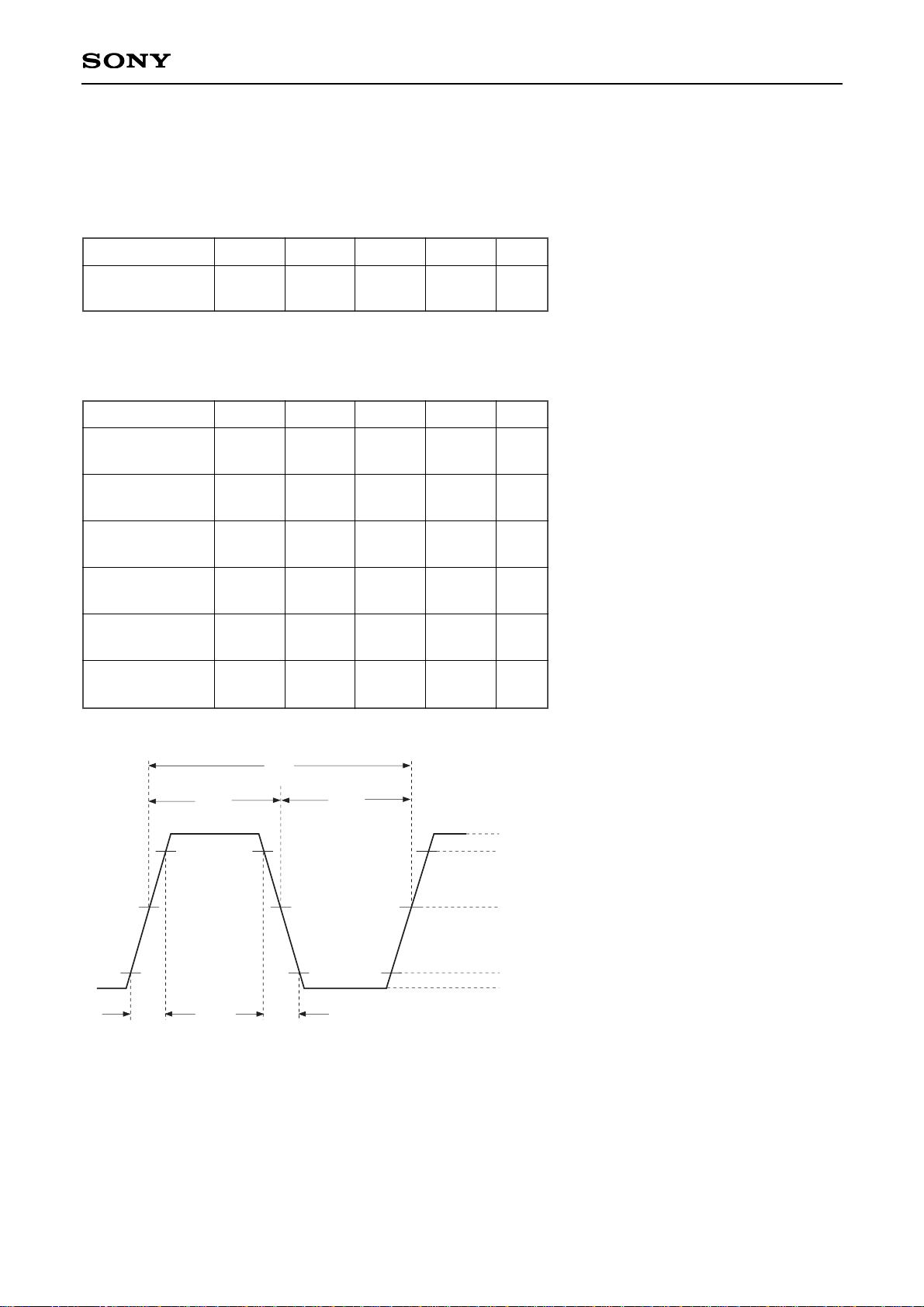
(1) XTAI pin
(a) When using self-excited oscillation
(VDD = AVDD = 2.2 ± 0.2V and 3.3 ± 0.3V, Vss = AVss = 0V, Topr = –20 to +75°C)
(b) When inputting pulses to XTAI pin
(VDD = AVDD
= 2.2 ± 0.2V and 3.3 ± 0.3V, Vss = AVss = 0V, Topr = –20 to +75°C)
Note) When the pulse is input to the XTAI pin, be sure to input it via the capacitor.
Oscillation
frequency
f
MAX 734
MHz
Item Symbol Min. Typ. Max. Unit
High level pulse
width
tWHX
13 500
ns
Low level pulse
width
tWLX
13 500
ns
Pulse cycle
tCX
26 1000
ns
Input high level VIHX 0.7VDD
V
Input low level VILX 0.2VDD
V
Rise time,
fall time
tR, tF
10
ns
Item
Symbol Min. Typ. Max. Unit
tR tF
tWHX
tWLX
tCX
VILX
VIHX × 0.1
V
IHX × 0.9
V
IHX
XTAI
VDD/2
Page 12
– 12 –
CXD3029R
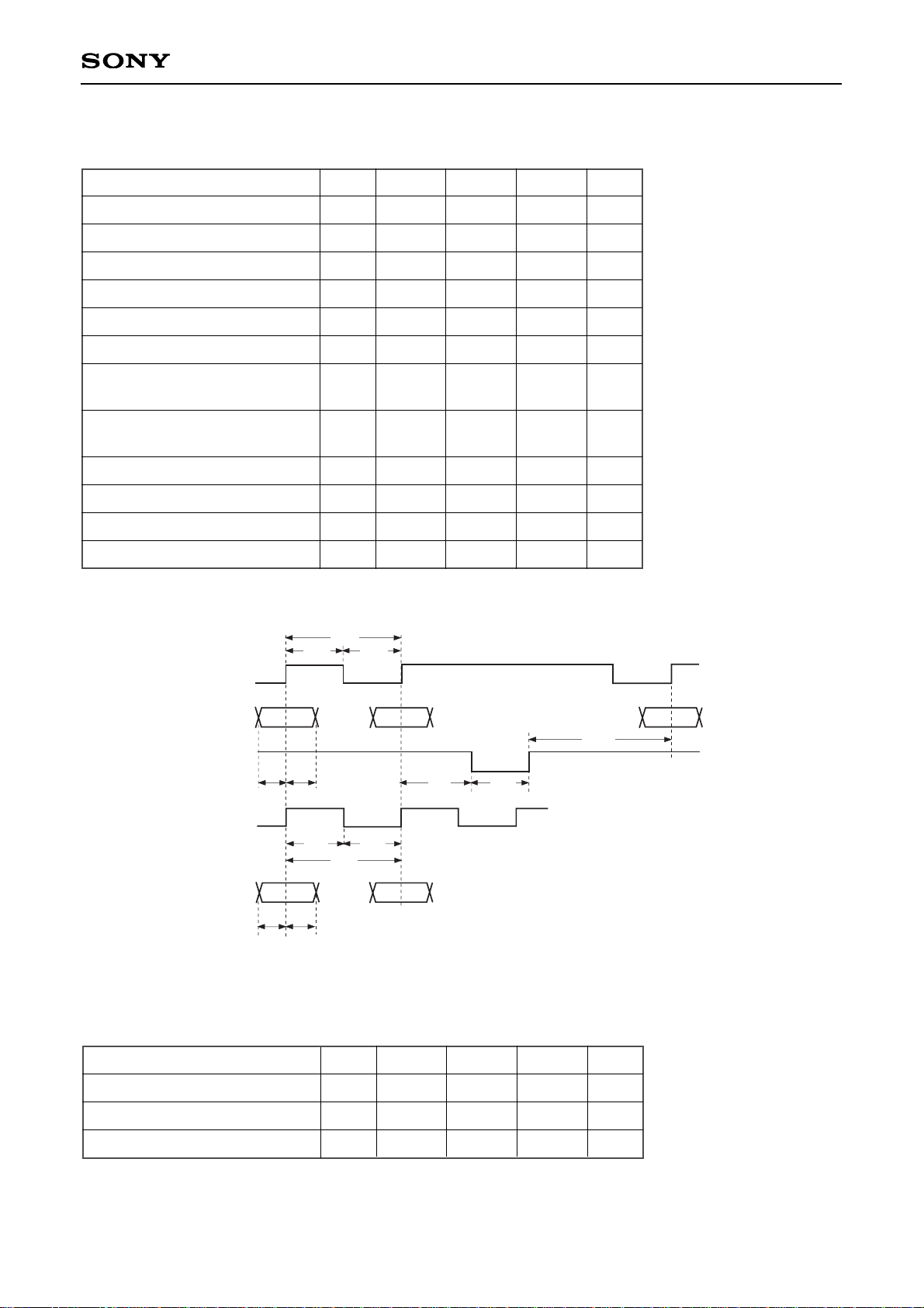
(2) CLOK, DATA, XLAT, SQCK and EXCK pins
(VDD = AVDD = 2.2 ± 0.2V and 3.3 ± 0.3V, VSS = AVSS = 0V, Topr = –22 to +75°C)
Clock frequency
Clock pulse width
Setup time
Hold time
Delay time
Latch pulse width
Latch pulse width
(during $AAX MLAT ON)
Command transfer interval
(during $AAX MLAT ON)
EXCK SQCK frequency
EXCK SQCK pulse width
COUT frequency (during input)
∗
COUT pulse width (during input)
∗
fCK
tWCK
t
SU
tH
tD
tWL
tWL
tWSC
fT
tWT
fT
tWT
750
300
300
300
750
6
11
750
7.5
0.65
30000
30000
0.65
65
MHz
ns
ns
ns
ns
ns
µs
µs
MHz
ns
kHz
µs
Item
Symbol Min.
Typ. Max. Unit
tWCK tWCK
1/fCK
tH
tSU
tWL
tD
1/fT
tWT tWT
tH
tSU
CLOK
DATA
XLAT
EXCK
SQCK
COUT
SBSO
SQSO
tWSC
∗
Only when $44 and $45 are executed.
(3) R4M pin (when $A4X CKOUTSL2 = CKOUTSL1 = 0)
(V
DD = AVDD = 2.2 ± 0.2V and 3.3 ± 0.3V, VSS = AVSS = 0V, Topr = –22 to +75°C)
Output frequency
Output duty
Output amplitude
fOUT
DOUT
VOUT
4.2336
50
VDD
MHz
%
V
Item
Symbol Min.
Typ. Max. Unit
Page 13
– 13 –
CXD3029R
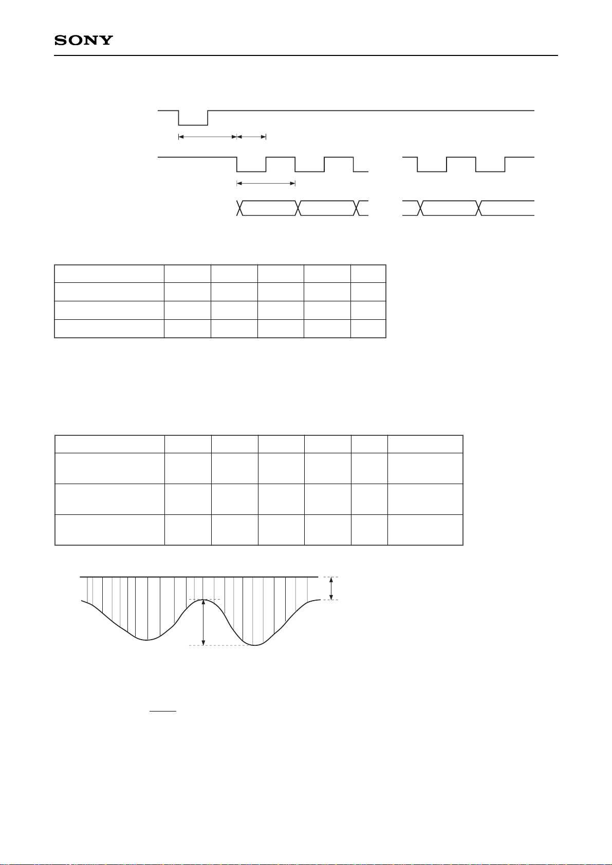
(4) SCLK pin
SCLK frequency
SCLK pulse width
Delay time
fSCLK
tSPW
tDLS
31.3
15
16 MHz
ns
µs
Item
Symbol
Min. Typ.
Max. Unit
(5) COUT, MIRR and DFCT pins
Operating frequency
(VDD = AVDD = 2.2 ± 0.2V and 3.3 ± 0.3V, VSS = AVSS = 0V, Topr = –20 to +75°C)
COUT maximum
operating frequency
MIRR maximum
operating frequency
DFCT maximum
operating frequency
fCOUT
fMIRR
fDFCTH
40
40
5
kHz
kHz
kHz
∗1
∗2
∗3
Signal
Symbol Min. Typ. Max.
Unit
Conditions
∗1
When using a high-speed traverse TZC.
∗2
When the RF signal continuously satisfies the following conditions during the above traverse.
• A = 0.11VDD to 0.23VDD
• ≤ 25%
∗3
During complete RF signal omission.
When settings related to DFCT signal generation are Typ.
A
B
B
A + B
(VDD = AVDD = 2.2 ± 0.2V and 3.3 ± 0.3V, VSS = AVSS = 0V, Topr = –20 to +75°C)
XLAT
tSPWtDLS
SCLK
Serial Read Out Data
(SENS)
1/fSCLK
MSB LSB
...
...
Page 14
– 14 –
CXD3029R
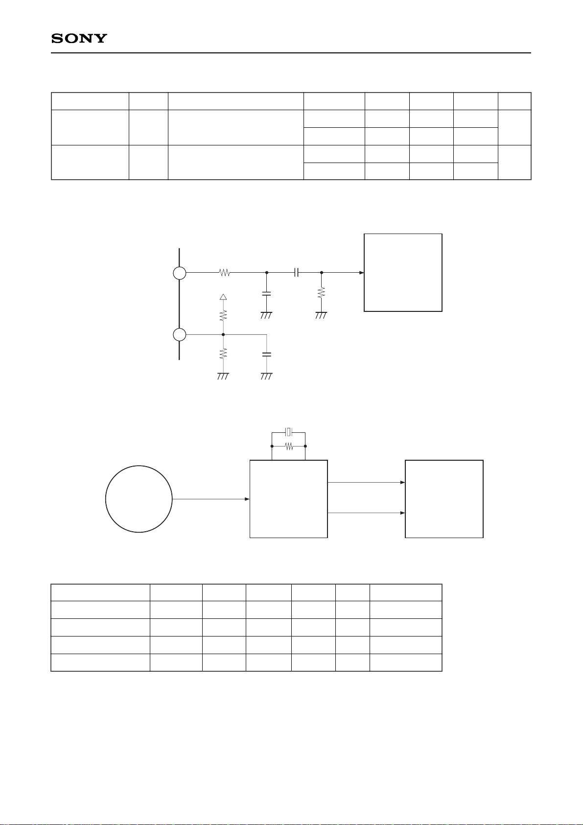
Fs = 44.1kHz in all cases.
The total harmonic distortion and signal-to-noise ratio measurement circuits are shown below.
1-bit DAC and LPF Block Analog Characteristics (VDD = AVDD = 3.3V, VSS = AVSS = 0V, Ta = 25°C)
Item
Total harmonic
distortion
Signal-to-noise
ratio
Symbol
THD
S/N
Conditions
1kHz, 0dB data
Crystal
1kHz, 0dB data, AMUT OFF
(Using A-weighting filter)
384Fs
768Fs
384Fs
768Fs
93
93
0.006
0.006
95
95
0.008
0.008
Min.
Typ.
Max.
Unit
%
dB
SHIBASOKU (AM51A)
22kΩ
22µF
AOUT1 (2)
VREFL (R)
22kΩ
10µF
220Ω
0.01µF
100kΩ
Audio Analyzer
Audio Analyzer
CXD3029R
Rch A
Lch B
DATA RF
TEST DISC
768Fs/384Fs
(VDD = AVDD = 3.3V, VSS = AVSS = 0V, Ta = –20 to +75°C)
V
OUT
RL
RVREF
CVREF
100
∗
1
∗1
∗2
∗2
Vrms
kΩ
kΩ
µF
Symbol
10
Min.
Max.
0.80
1
Typ.
Applicable pinsUnit
Output voltage
Load resistance
VREF pin resistance
VREF pin capacitance
Item
∗
Measurement is conducted for the above circuit diagrams with the sine wave output of 1kHz and 0dB.
Applicable pins
∗∗
1
AOUT1, AOUT2
∗∗
2
VREFL, VREFR
Block diagram of analog characteristics measurement
LPF external circuit diagram
Page 15

– 15 –
CXD3029R
Contents
[1] CPU Interface
§1-1. CPU Interface Timing . . . . . . . . . . . . . . . . . . . . . . . . . . . . . . . . . . . . . . . . . . . . . . . . . . . . . . . . . . 16
§1-2. CPU Interface Command Table . . . . . . . . . . . . . . . . . . . . . . . . . . . . . . . . . . . . . . . . . . . . . . . . . . 16
§1-3. CPU Command Presets . . . . . . . . . . . . . . . . . . . . . . . . . . . . . . . . . . . . . . . . . . . . . . . . . . . . . . . . 31
§1-4. Description of SENS Signals . . . . . . . . . . . . . . . . . . . . . . . . . . . . . . . . . . . . . . . . . . . . . . . . . . . . . 41
§1-5. Description of Commands . . . . . . . . . . . . . . . . . . . . . . . . . . . . . . . . . . . . . . . . . . . . . . . . . . . . . . . 43
[2] Subcode Interface
§2-1. P to W Subcode Readout . . . . . . . . . . . . . . . . . . . . . . . . . . . . . . . . . . . . . . . . . . . . . . . . . . . . . . . 95
§2-2. 80-bit Subcode-Q Readout . . . . . . . . . . . . . . . . . . . . . . . . . . . . . . . . . . . . . . . . . . . . . . . . . . . . . . 95
[3] Description of Modes
§3-1. CLV-N Mode . . . . . . . . . . . . . . . . . . . . . . . . . . . . . . . . . . . . . . . . . . . . . . . . . . . . . . . . . . . . . . . . 102
§3-2. CLV-W Mode . . . . . . . . . . . . . . . . . . . . . . . . . . . . . . . . . . . . . . . . . . . . . . . . . . . . . . . . . . . . . . . . 102
§3-3. CAV-W Mode . . . . . . . . . . . . . . . . . . . . . . . . . . . . . . . . . . . . . . . . . . . . . . . . . . . . . . . . . . . . . . . . 102
§3-4. VCO-C Mode . . . . . . . . . . . . . . . . . . . . . . . . . . . . . . . . . . . . . . . . . . . . . . . . . . . . . . . . . . . . . . . . 103
[4] Description of Other Functions
§4-1. Channel Clock Recovery by Digital PLL Circuit . . . . . . . . . . . . . . . . . . . . . . . . . . . . . . . . . . . . . . 106
§4-2. Frame Sync Protection . . . . . . . . . . . . . . . . . . . . . . . . . . . . . . . . . . . . . . . . . . . . . . . . . . . . . . . . 108
§4-3. Error Correction . . . . . . . . . . . . . . . . . . . . . . . . . . . . . . . . . . . . . . . . . . . . . . . . . . . . . . . . . . . . . . 108
§4-4. DA Interface . . . . . . . . . . . . . . . . . . . . . . . . . . . . . . . . . . . . . . . . . . . . . . . . . . . . . . . . . . . . . . . . . 109
§4-5. Digital Out . . . . . . . . . . . . . . . . . . . . . . . . . . . . . . . . . . . . . . . . . . . . . . . . . . . . . . . . . . . . . . . . . . 112
§4-6. Servo Auto Sequence . . . . . . . . . . . . . . . . . . . . . . . . . . . . . . . . . . . . . . . . . . . . . . . . . . . . . . . . . 118
§4-7. Digital CLV . . . . . . . . . . . . . . . . . . . . . . . . . . . . . . . . . . . . . . . . . . . . . . . . . . . . . . . . . . . . . . . . . . 126
§4-8. CD-DSP Block Playback Speed . . . . . . . . . . . . . . . . . . . . . . . . . . . . . . . . . . . . . . . . . . . . . . . . . 127
§4-9. Description of DAC Block and Shock-proof Memory Controller Block Circuits . . . . . . . . . . . . . . 127
§4-10. DAC Block Input Timing . . . . . . . . . . . . . . . . . . . . . . . . . . . . . . . . . . . . . . . . . . . . . . . . . . . . . . . 128
§4-11. Description of DAC Block Functions . . . . . . . . . . . . . . . . . . . . . . . . . . . . . . . . . . . . . . . . . . . . . . 129
§4-12. LPF Block . . . . . . . . . . . . . . . . . . . . . . . . . . . . . . . . . . . . . . . . . . . . . . . . . . . . . . . . . . . . . . . . . . 134
§4-13. Description of Shock-proof Memory Controller Block Functions . . . . . . . . . . . . . . . . . . . . . . . . . 135
§4-14. CPU to DRAM Access Function . . . . . . . . . . . . . . . . . . . . . . . . . . . . . . . . . . . . . . . . . . . . . . . . . 140
§4-15. Asymmetry Correction . . . . . . . . . . . . . . . . . . . . . . . . . . . . . . . . . . . . . . . . . . . . . . . . . . . . . . . . . 144
§4-16. CD TEXT Data Demodulation . . . . . . . . . . . . . . . . . . . . . . . . . . . . . . . . . . . . . . . . . . . . . . . . . . . 145
[5] Description of Servo Signal Processing System Functions and Commands
§5-1. General Description of Servo Signal Processing System . . . . . . . . . . . . . . . . . . . . . . . . . . . . . . 147
§5-2. Digital Servo Block Master Clock (MCK) . . . . . . . . . . . . . . . . . . . . . . . . . . . . . . . . . . . . . . . . . . . 148
§5-3. DC Offset Cancel [AVRG Measurement and Compensation] . . . . . . . . . . . . . . . . . . . . . . . . . . . 149
§5-4. E:F Balance Adjustment Function . . . . . . . . . . . . . . . . . . . . . . . . . . . . . . . . . . . . . . . . . . . . . . . . 150
§5-5. FCS Bias Adjustment Function . . . . . . . . . . . . . . . . . . . . . . . . . . . . . . . . . . . . . . . . . . . . . . . . . . 150
§5-6. AGCNTL Function . . . . . . . . . . . . . . . . . . . . . . . . . . . . . . . . . . . . . . . . . . . . . . . . . . . . . . . . . . . . 152
§5-7. FCS Servo and FCS Search . . . . . . . . . . . . . . . . . . . . . . . . . . . . . . . . . . . . . . . . . . . . . . . . . . . . 154
§5-8. TRK and SLD Servo Control . . . . . . . . . . . . . . . . . . . . . . . . . . . . . . . . . . . . . . . . . . . . . . . . . . . . 155
§5-9. MIRR and DFCT Signal Generation . . . . . . . . . . . . . . . . . . . . . . . . . . . . . . . . . . . . . . . . . . . . . . 156
§5-10. DFCT Countermeasure Circuit . . . . . . . . . . . . . . . . . . . . . . . . . . . . . . . . . . . . . . . . . . . . . . . . . . 157
§5-11. Anti-shock Circuit . . . . . . . . . . . . . . . . . . . . . . . . . . . . . . . . . . . . . . . . . . . . . . . . . . . . . . . . . . . . . 157
§5-12. Brake Circuit . . . . . . . . . . . . . . . . . . . . . . . . . . . . . . . . . . . . . . . . . . . . . . . . . . . . . . . . . . . . . . . . 158
§5-13. COUT Signal . . . . . . . . . . . . . . . . . . . . . . . . . . . . . . . . . . . . . . . . . . . . . . . . . . . . . . . . . . . . . . . . 159
§5-14. Serial Readout Circuit . . . . . . . . . . . . . . . . . . . . . . . . . . . . . . . . . . . . . . . . . . . . . . . . . . . . . . . . . 159
§5-15. Writing to Coefficient RAM . . . . . . . . . . . . . . . . . . . . . . . . . . . . . . . . . . . . . . . . . . . . . . . . . . . . . 160
§5-16. PWM Output . . . . . . . . . . . . . . . . . . . . . . . . . . . . . . . . . . . . . . . . . . . . . . . . . . . . . . . . . . . . . . . . 160
§5-17. Servo Status Changes Produced by LOCK Signal . . . . . . . . . . . . . . . . . . . . . . . . . . . . . . . . . . . 161
§5-18. Description of Commands and Data Sets . . . . . . . . . . . . . . . . . . . . . . . . . . . . . . . . . . . . . . . . . . 161
§5-19. List of Servo Filter Coefficients . . . . . . . . . . . . . . . . . . . . . . . . . . . . . . . . . . . . . . . . . . . . . . . . . . 189
§5-20. Filter Composition . . . . . . . . . . . . . . . . . . . . . . . . . . . . . . . . . . . . . . . . . . . . . . . . . . . . . . . . . . . . 191
§5-21. TRACKING and FOCUS Frequency Response . . . . . . . . . . . . . . . . . . . . . . . . . . . . . . . . . . . . . 197
[6] Application Circuit . . . . . . . . . . . . . . . . . . . . . . . . . . . . . . . . . . . . . . . . . . . . . . . . . . . . . . . . . . . . . . . . 198
Explanation of abbreviations
AVRG: Average
AGCNTL: Auto gain control
FCS: Focus
TRK: Tracking
SLD: Sled
DFCT: Defect
Page 16
– 16 –
CXD3029R
[1] CPU Interface
§1-1. CPU Interface Timing
• CPU interface
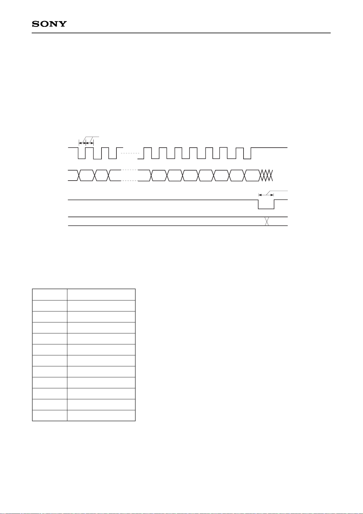
This interface uses DATA, CLOK and XLAT to set the modes.
The interface timing chart is shown below. (See 2. AC Characteristics in Electrical Characteristics, for the
details of the AC characteristics.)
• The internal registers are initialized by a reset when XRST = 0.
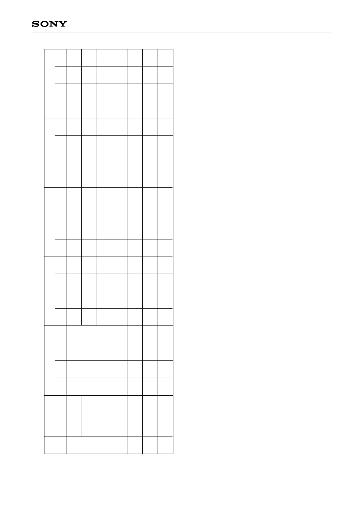
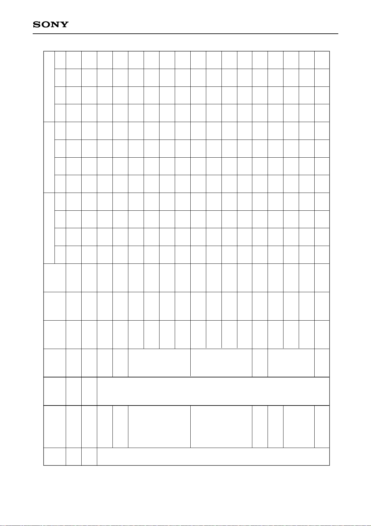
§1-2. CPU Interface Command Table
Total bit length for each register
Register
0 to 2
3
4 to 6
7
8
9
A
B
C
D
E
8 bits
8 to 24 bits
16 bits
20 bits
32 bits
32 bits
28 bits
28 bits
28 bits
28 bits
20 bits
Total bit length
750ns to 30µs
D18 D19 D20 D21 D22 D23
750ns or more
(6µs or more
when $AAX
MLAT ON)
Valid
CLOK
DATA
XLAT
Registers
D0 D1
Page 17
– 17 –
CXD3029R
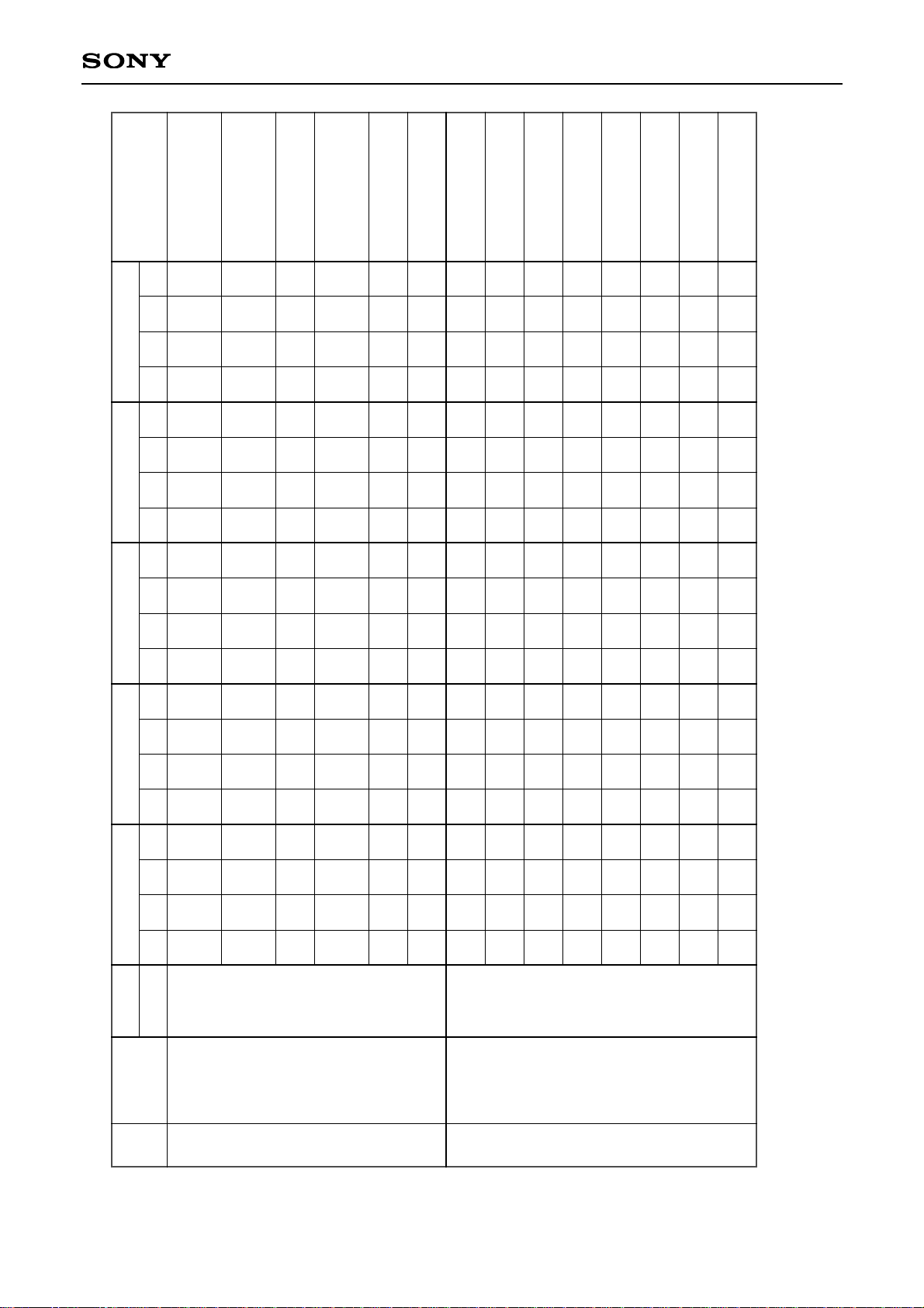
FOCUS SERVO ON
(FOCUS GAIN
NORMAL)
FOCUS SERVO ON
(FOCUS GAIN
DOWN)
FOCUS SERVO OFF,
0V OUT
FOCUS SERVO OFF,
FOCUS SEARCH
VOLTAGE OUT
FOCUS SEARCH
VOLTAGE DOWN
FOCUS SEARCH
VOLTAGE UP
ANTI SHOCK ON
ANTI SHOCK OFF
BRAKE ON
BRAKE OFF
TRACKING GAIN
NORMAL
TRACKING GAIN UP
TRACKING GAIN UP
FILTER SELECT 1
TRACKING GAIN UP
FILTER SELECT 2
1
1
0
0
0
0
1
0
—
—
—
—
—
—
0
1
—
—
—
—
0
—
1
0
—
—
—
—
—
—
0
1
1
1
—
—
—
—
0
1
—
—
—
—
—
—
0
1
—
—
—
—
—
—
1
0
—
—
—
—
—
—
—
—
—
—
—
—
—
—
—
—
—
—
—
—
—
—
—
—
—
—
—
—
—
—
—
—
—
—
—
—
—
—
—
—
—
—
—
—
—
—
—
—
—
—
—
—
—
—
—
—
—
—
—
—
—
—
—
—
—
—
—
—
—
—
—
—
—
—
—
—
—
—
—
—
—
—
—
—
—
—
—
—
—
—
—
—
—
—
—
—
—
—
—
—
—
—
—
—
—
—
—
—
—
—
—
—
—
—
—
—
—
—
—
—
—
—
—
—
—
—
—
—
—
—
—
—
—
—
—
—
—
—
—
—
—
—
—
—
—
—
—
—
—
—
—
—
—
—
—
—
—
—
—
—
—
—
—
—
—
—
—
—
—
—
—
—
—
—
—
—
—
—
—
—
—
—
—
—
—
—
—
—
—
—
—
—
—
—
—
—
—
—
—
—
—
—
—
—
—
—
—
—
—
—
—
—
—
—
—
—
—
—
—
—
—
—
—
—
0
1
0 0 0 0
0 0 0 1
FOCUS
CONTROL
TRACKING
CONTROL
Regis-
ter
Command
Address
D23 to D20
Data 1
D19 D18 D17 D16
Data 2
D15 D14 D13 D12
Data 3
D11 D10 D9 D8
Data 4
D7 D6 D5 D4
Data 5
D3 D2 D1 D0
Command Table ($0X to 1X)
—: don’t care
Page 18
– 18 –
CXD3029R
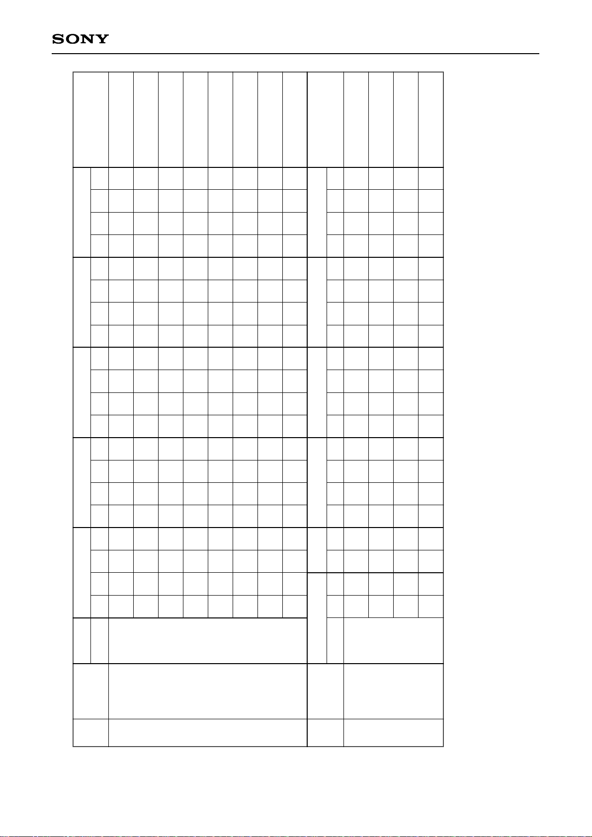
TRACKING SERVO OFF
TRACKING SERVO ON
FORWARD TRACK JUMP
REVERSE TRACK JUMP
SLED SERVO OFF
SLED SERVO ON
FORWARD SLED MOVE
REVERSE SLED MOVE
SLED KICK LEVEL
(±1 × basic value) (default)
SLED KICK LEVEL
(±2 × basic value)
SLED KICK LEVEL
(±3 × basic value)
SLED KICK LEVEL
(±4 × basic value)
0
0
1
1
—
—
—
—
0
0
0
0
0
0
0
0
0
0
1
1
0
1
0
1
—
—
—
—
—
—
—
—
—
—
—
—
—
—
—
—
—
—
—
—
—
—
—
—
—
—
—
—
—
—
—
—
—
—
—
—
—
—
—
—
—
—
—
—
—
—
—
—
—
—
—
—
—
—
—
—
—
—
—
—
—
—
—
—
0
1
0
1
—
—
—
—
—
—
—
—
0
0
1
1
—
—
—
—
0
1
0
1
—
—
—
—
—
—
—
—
—
—
—
—
—
—
—
—
—
—
—
—
—
—
—
—
—
—
—
—
—
—
—
—
—
—
—
—
—
—
—
—
—
—
—
—
—
—
—
—
—
—
—
—
—
—
—
—
—
—
—
—
—
—
—
—
—
—
—
—
—
—
—
—
—
—
—
—
—
—
—
—
—
—
—
—
—
—
—
—
—
—
—
—
—
—
—
—
—
—
—
—
—
—
—
—
—
—
—
—
—
—
—
—
—
—
—
—
—
—
—
—
—
—
—
—
—
—
—
—
2
3
0 0 1 0
0 0 1 1
TRACKING
MODE
SELECT
Regis-
ter
Command
Address
D23 to D20
Regis-
ter
Command
Address
D23 to D20
Data 1
D19 D18 D17 D16
Data 1
D19 D18 D17 D16
Data 2
D15 D14 D13 D12
Data 2
D15 D14 D13 D12
Data 3
D11 D10 D9 D8
Data 4
D7 D6 D5 D4
Data 5
D3 D2 D1 D0
Data 3
D11 D10 D9 D8
Data 4
D7 D6 D5 D4
Data 5
D3 D2 D1 D0
—: don’t care
Command Table ($2X to 3X)
Page 19
– 19 –
CXD3029R
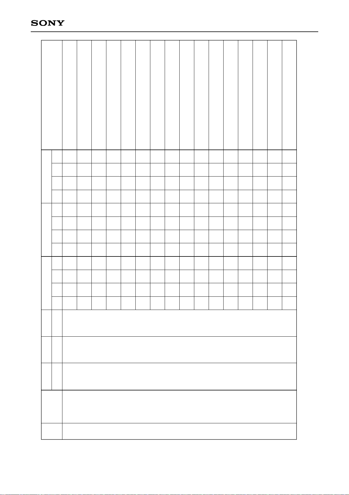
KRAM DATA (K00)
SLED INPUT GAIN
KRAM DATA (K01)
SLED LOW BOOST FILTER A-H
KRAM DATA (K02)
SLED LOW BOOST FILTER A-L
KRAM DATA (K03)
SLED LOW BOOST FILTER B-H
KRAM DATA (K04)
SLED LOW BOOST FILTER B-L
KRAM DATA (K05)
SLED OUTPUT GAIN
KRAM DATA (K06)
FOCUS INPUT GAIN
KRAM DATA (K07)
SLED AUTO GAIN
KRAM DATA (K08)
FOCUS HIGH CUT FILTER A
KRAM DATA (K09)
FOCUS HIGH CUT FILTER B
KRAM DATA (K0A)
FOCUS LOW BOOST FILTER A-H
KRAM DATA (K0B)
FOCUS LOW BOOST FILTER A-L
KRAM DATA (K0C)
FOCUS LOW BOOST FILTER B-H
KRAM DATA (K0D)
FOCUS LOW BOOST FILTER B-L
KRAM DATA (K0E)
FOCUS PHASE COMPENSATE FILTER A
KRAM DATA (K0F)
FOCUS DEFECT HOLD GAIN
0
0
0
0
0
0
0
0
1
1
1
1
1
1
1
1
0
0
0
0
1
1
1
1
0
0
0
0
1
1
1
1
0
0
1
1
0
0
1
1
0
0
1
1
0
0
1
1
0
1
0
1
0
1
0
1
0
1
0
1
0
1
0
1
KD7
KD7
KD7
KD7
KD7
KD7
KD7
KD7
KD7
KD7
KD7
KD7
KD7
KD7
KD7
KD7
KD6
KD6
KD6
KD6
KD6
KD6
KD6
KD6
KD6
KD6
KD6
KD6
KD6
KD6
KD6
KD6
KD5
KD5
KD5
KD5
KD5
KD5
KD5
KD5
KD5
KD5
KD5
KD5
KD5
KD5
KD5
KD5
KD4
KD4
KD4
KD4
KD4
KD4
KD4
KD4
KD4
KD4
KD4
KD4
KD4
KD4
KD4
KD4
KD3
KD3
KD3
KD3
KD3
KD3
KD3
KD3
KD3
KD3
KD3
KD3
KD3
KD3
KD3
KD3
KD2
KD2
KD2
KD2
KD2
KD2
KD2
KD2
KD2
KD2
KD2
KD2
KD2
KD2
KD2
KD2
KD1
KD1
KD1
KD1
KD1
KD1
KD1
KD1
KD1
KD1
KD1
KD1
KD1
KD1
KD1
KD1
KD0
KD0
KD0
KD0
KD0
KD0
KD0
KD0
KD0
KD0
KD0
KD0
KD0
KD0
KD0
KD0
3 0 0 1 1 0 1 0 0 0 0 0 0SELECT
Regis-
ter
Command
Address 1
D23 to D20
Address 2
D19 to D16
Address 3
D15 to D12
Address 4
D11 D10 D9 D8
Data 1
D7 D6 D5 D4
Data 2
D3 D2 D1 D0
Command Table ($340X)
Page 20
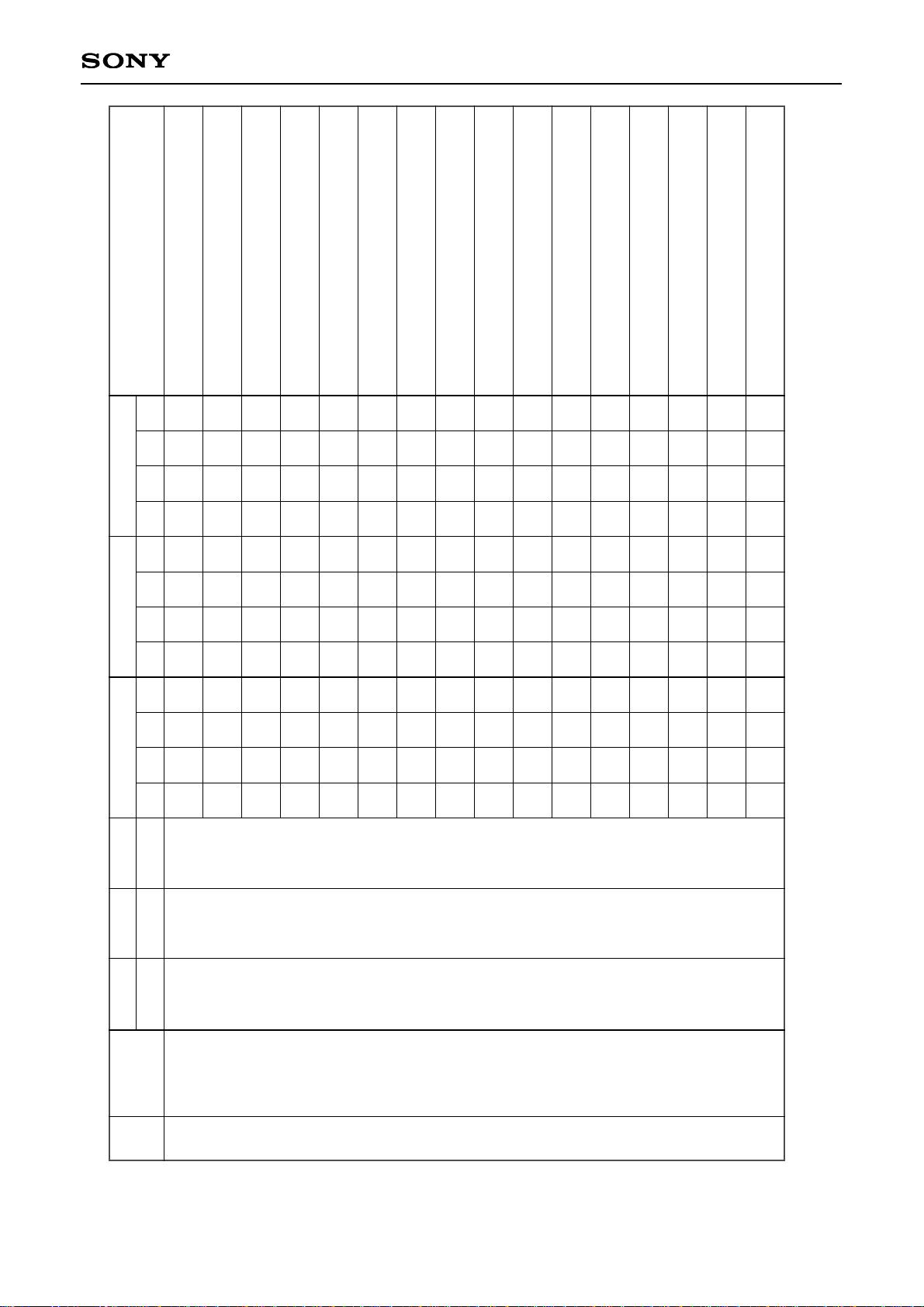
– 20 –
CXD3029R
KRAM DATA (K10)
FOCUS PHASE COMPENSATE FILTER B
KRAM DATA (K11)
FOCUS OUTPUT GAIN
KRAM DATA (K12)
ANTI SHOCK INPUT GAIN
KRAM DATA (K13)
FOCUS AUTO GAIN
KRAM DATA (K14)
HPTZC / AUTO GAIN HIGH PASS FILTER A
KRAM DATA (K15)
HPTZC / AUTO GAIN HIGH PASS FILTER B
KRAM DATA (K16)
ANTI SHOCK HIGH PASS FILTER A
KRAM DATA (K17)
HPTZC / AUTO GAIN LOW PASS FILTER B
KRAM DATA (K18)
FIX
KRAM DATA (K19)
TRACKING INPUT GAIN
KRAM DATA (K1A)
TRACKING HIGH CUT FILTER A
KRAM DATA (K1B)
TRACKING HIGH CUT FILTER B
KRAM DATA (K1C)
TRACKING LOW BOOST FILTER A-H
KRAM DATA (K1D)
TRACKING LOW BOOST FILTER A-L
KRAM DATA (K1E)
TRACKING LOW BOOST FILTER B-H
KRAM DATA (K1F)
TRACKING LOW BOOST FILTER B-L
0
0
0
0
0
0
0
0
1
1
1
1
1
1
1
1
0
0
0
0
1
1
1
1
0
0
0
0
1
1
1
1
0
0
1
1
0
0
1
1
0
0
1
1
0
0
1
1
0
1
0
1
0
1
0
1
0
1
0
1
0
1
0
1
KD7
KD7
KD7
KD7
KD7
KD7
KD7
KD7
KD7
KD7
KD7
KD7
KD7
KD7
KD7
KD7
KD6
KD6
KD6
KD6
KD6
KD6
KD6
KD6
KD6
KD6
KD6
KD6
KD6
KD6
KD6
KD6
KD5
KD5
KD5
KD5
KD5
KD5
KD5
KD5
KD5
KD5
KD5
KD5
KD5
KD5
KD5
KD5
KD4
KD4
KD4
KD4
KD4
KD4
KD4
KD4
KD4
KD4
KD4
KD4
KD4
KD4
KD4
KD4
KD3
KD3
KD3
KD3
KD3
KD3
KD3
KD3
KD3
KD3
KD3
KD3
KD3
KD3
KD3
KD3
KD2
KD2
KD2
KD2
KD2
KD2
KD2
KD2
KD2
KD2
KD2
KD2
KD2
KD2
KD2
KD2
KD1
KD1
KD1
KD1
KD1
KD1
KD1
KD1
KD1
KD1
KD1
KD1
KD1
KD1
KD1
KD1
KD0
KD0
KD0
KD0
KD0
KD0
KD0
KD0
KD0
KD0
KD0
KD0
KD0
KD0
KD0
KD0
3 0 0 1 1 0 1 0 0 0 0 0 1SELECT
Regis-
ter
Command
Address 1
D23 to D20
Address 2
D19 to D16
Address 3
D15 to D12
Address 4
D11 D10 D9 D8
Data 1
D7 D6 D5 D4
Data 2
D3 D2 D1 D0
Command Table ($341X)
Page 21
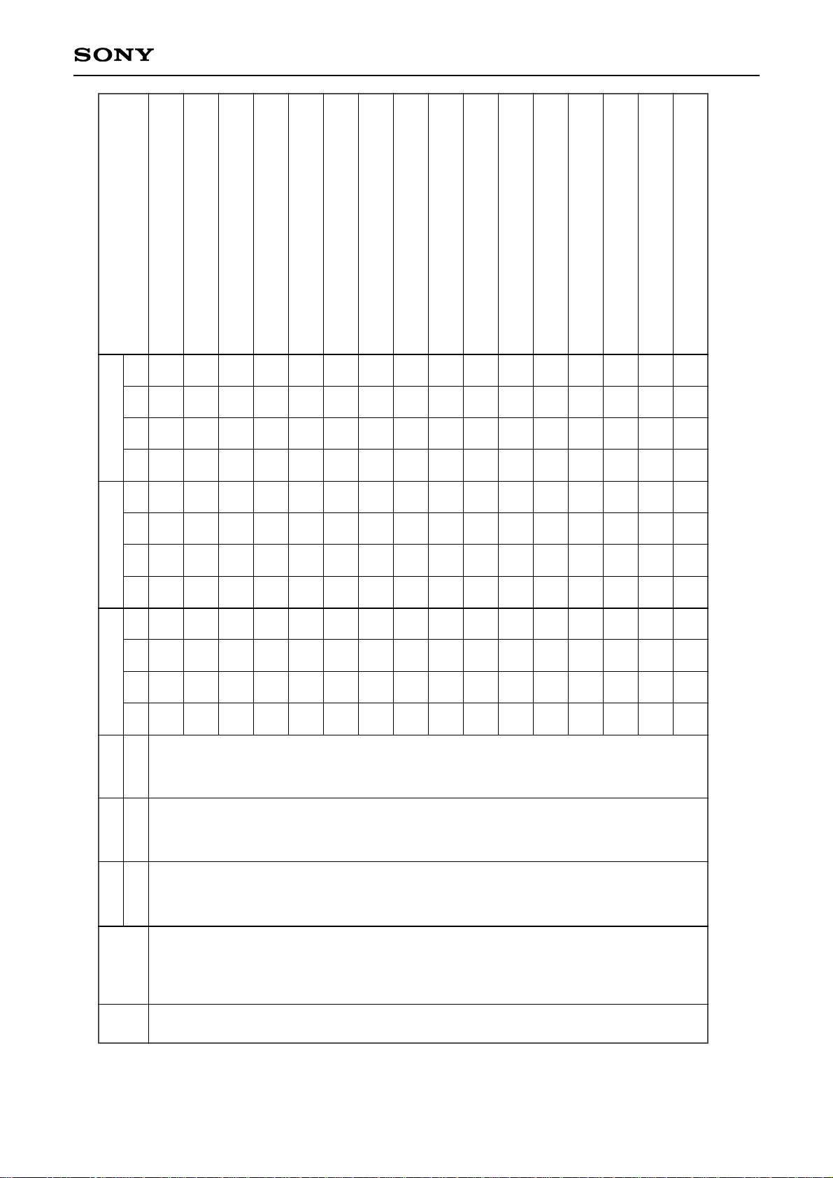
– 21 –
CXD3029R
KRAM DATA (K20)
TRACKING PHASE COMPENSATE FILTER A
KRAM DATA (K21)
TRACKING PHASE COMPENSATE FILTER B
KRAM DATA (K22)
TRACKING OUTPUT GAIN
KRAM DATA (K23)
TRACKING AUTO GAIN
KRAM DATA (K24)
FOCUS GAIN DOWN HIGH CUT FILTER A
KRAM DATA (K25)
FOCUS GAIN DOWN HIGH CUT FILTER B
KRAM DATA (K26)
FOCUS GAIN DOWN LOW BOOST FILTER A-H
KRAM DATA (K27)
FOCUS GAIN DOWN LOW BOOST FILTER A-L
KRAM DATA (K28)
FOCUS GAIN DOWN LOW BOOST FILTER B-H
KRAM DATA (K29)
FOCUS GAIN DOWN LOW BOOST FILTER B-L
KRAM DATA (K2A)
FOCUS GAIN DOWN PHASE COMPENSATE FILTER A
KRAM DATA (K2B)
FOCUS GAIN DOWN DEFECT HOLD GAIN
KRAM DATA (K2C)
FOCUS GAIN DOWN PHASE COMPENSATE FILTER B
KRAM DATA (K2D)
FOCUS GAIN DOWN OUTPUT GAIN
KRAM DATA (K2E)
Not used
KRAM DATA (K2F)
Not used
0
0
0
0
0
0
0
0
1
1
1
1
1
1
1
1
0
0
0
0
1
1
1
1
0
0
0
0
1
1
1
1
0
0
1
1
0
0
1
1
0
0
1
1
0
0
1
1
0
1
0
1
0
1
0
1
0
1
0
1
0
1
0
1
KD7
KD7
KD7
KD7
KD7
KD7
KD7
KD7
KD7
KD7
KD7
KD7
KD7
KD7
KD7
KD7
KD6
KD6
KD6
KD6
KD6
KD6
KD6
KD6
KD6
KD6
KD6
KD6
KD6
KD6
KD6
KD6
KD5
KD5
KD5
KD5
KD5
KD5
KD5
KD5
KD5
KD5
KD5
KD5
KD5
KD5
KD5
KD5
KD4
KD4
KD4
KD4
KD4
KD4
KD4
KD4
KD4
KD4
KD4
KD4
KD4
KD4
KD4
KD4
KD3
KD3
KD3
KD3
KD3
KD3
KD3
KD3
KD3
KD3
KD3
KD3
KD3
KD3
KD3
KD3
KD2
KD2
KD2
KD2
KD2
KD2
KD2
KD2
KD2
KD2
KD2
KD2
KD2
KD2
KD2
KD2
KD1
KD1
KD1
KD1
KD1
KD1
KD1
KD1
KD1
KD1
KD1
KD1
KD1
KD1
KD1
KD1
KD0
KD0
KD0
KD0
KD0
KD0
KD0
KD0
KD0
KD0
KD0
KD0
KD0
KD0
KD0
KD0
3 0 0 1 1 0 1 0 0 0 0 1 0SELECT
Regis-
ter
Command
Address 1
D23 to D20
Address 2
D19 to D16
Address 3
D15 to D12
Address 4
D11 D10 D9 D8
Data 1
D7 D6 D5 D4
Data 2
D3 D2 D1 D0
Command Table ($342X)
Page 22
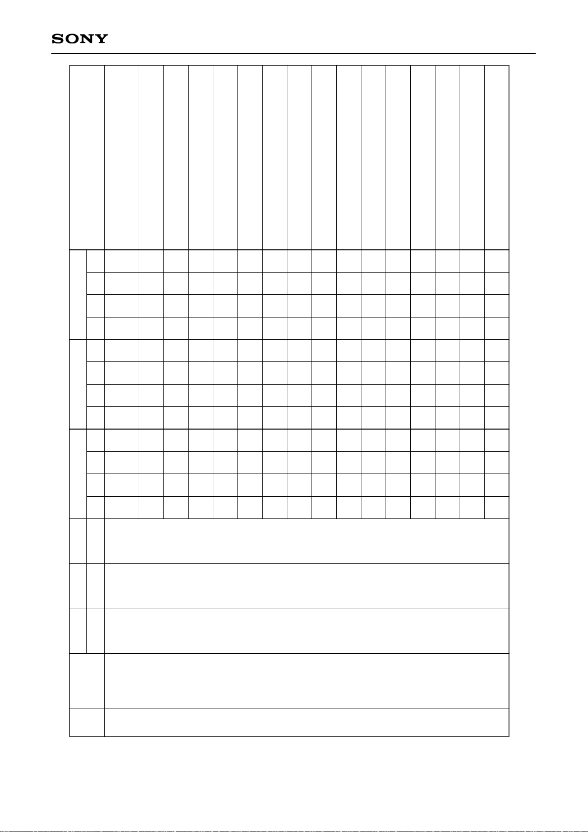
– 22 –
CXD3029R
KRAM DATA (K30)
SLED INPUT GAIN (when TGup2 is accessed with
SFSK = 1)
KRAM DATA (K31)
ANTI SHOCK LOW PASS FILTER B
KRAM DATA (K32)
Not used
KRAM DATA (K33)
ANTI SHOCK HIGH PASS FILTER B-H
KRAM DATA (K34)
ANTI SHOCK HIGH PASS FILTER B-L
KRAM DATA (K35)
ANTI SHOCK FILTER COMPARATE GAIN
KRAM DATA (K36)
TRACKING GAIN UP2 HIGH CUT FILTER A
KRAM DATA (K37)
TRACKING GAIN UP2 HIGH CUT FILTER B
KRAM DATA (K38)
TRACKING GAIN UP2 LOW BOOST FILTER A-H
KRAM DATA (K39)
TRACKING GAIN UP2 LOW BOOST FILTER A-L
KRAM DATA (K3A)
TRACKING GAIN UP2 LOW BOOST FILTER B-H
KRAM DATA (K3B)
TRACKING GAIN UP2 LOW BOOST FILTER B-L
KRAM DATA (K3C)
TRACKING GAIN UP PHASE COMPENSATE FILTER A
KRAM DATA (K3D)
TRACKING GAIN UP PHASE COMPENSATE FILTER B
KRAM DATA (K3E)
TRACKING GAIN UP OUTPUT GAIN
KRAM DATA (K3F)
Not used
0
0
0
0
0
0
0
0
1
1
1
1
1
1
1
1
0
0
0
0
1
1
1
1
0
0
0
0
1
1
1
1
0
0
1
1
0
0
1
1
0
0
1
1
0
0
1
1
0
1
0
1
0
1
0
1
0
1
0
1
0
1
0
1
KD7
KD7
KD7
KD7
KD7
KD7
KD7
KD7
KD7
KD7
KD7
KD7
KD7
KD7
KD7
KD7
KD6
KD6
KD6
KD6
KD6
KD6
KD6
KD6
KD6
KD6
KD6
KD6
KD6
KD6
KD6
KD6
KD5
KD5
KD5
KD5
KD5
KD5
KD5
KD5
KD5
KD5
KD5
KD5
KD5
KD5
KD5
KD5
KD4
KD4
KD4
KD4
KD4
KD4
KD4
KD4
KD4
KD4
KD4
KD4
KD4
KD4
KD4
KD4
KD3
KD3
KD3
KD3
KD3
KD3
KD3
KD3
KD3
KD3
KD3
KD3
KD3
KD3
KD3
KD3
KD2
KD2
KD2
KD2
KD2
KD2
KD2
KD2
KD2
KD2
KD2
KD2
KD2
KD2
KD2
KD2
KD1
KD1
KD1
KD1
KD1
KD1
KD1
KD1
KD1
KD1
KD1
KD1
KD1
KD1
KD1
KD1
KD0
KD0
KD0
KD0
KD0
KD0
KD0
KD0
KD0
KD0
KD0
KD0
KD0
KD0
KD0
KD0
3 0 0 1 1 0 1 0 0 0 0 1 1SELECT
Regis-
ter
Command
Address 1
D23 to D20
Address 2
D19 to D16
Address 3
D15 to D12
Address 4
D11 D10 D9 D8
Data 1
D7 D6 D5 D4
Data 2
D3 D2 D1 D0
Command Table ($343X)
Page 23
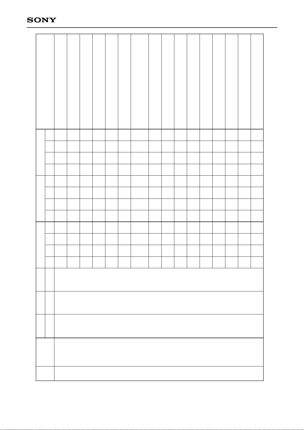
– 23 –
CXD3029R
KRAM DATA (K40)
TRACKING HOLD FILTER INPUT GAIN
KRAM DATA (K41)
TRACKING HOLD FILTER A-H
KRAM DATA (K42)
TRACKING HOLD FILTER A-L
KRAM DATA (K43)
TRACKING HOLD FILTER B-H
KRAM DATA (K44)
TRACKING HOLD FILTER B-L
KRAM DATA (K45)
TRACKING HOLD FILTER OUTPUT GAIN
KRAM DATA (K46)
TRACKING HOLD INPUT GAIN (when TGup2 is
accessed with THSK = 1)
KRAM DATA (K47)
Not used
KRAM DATA (K48)
FOCUS HOLD FILTER INPUT GAIN
KRAM DATA (K49)
FOCUS HOLD FILTER A-H
KRAM DATA (K4A)
FOCUS HOLD FILTER A-L
KRAM DATA (K4B)
FOCUS HOLD FILTER B-H
KRAM DATA (K4C)
FOCUS HOLD FILTER B-L
KRAM DATA (K4D)
FOCUS HOLD FILTER OUTPUT GAIN
KRAM DATA (K4E)
Not used
KRAM DATA (K4F)
Not used
0
0
0
0
0
0
0
0
1
1
1
1
1
1
1
1
0
0
0
0
1
1
1
1
0
0
0
0
1
1
1
1
0
0
1
1
0
0
1
1
0
0
1
1
0
0
1
1
0
1
0
1
0
1
0
1
0
1
0
1
0
1
0
1
KD7
KD7
KD7
KD7
KD7
KD7
KD7
KD7
KD7
KD7
KD7
KD7
KD7
KD7
KD7
KD7
KD6
KD6
KD6
KD6
KD6
KD6
KD6
KD6
KD6
KD6
KD6
KD6
KD6
KD6
KD6
KD6
KD5
KD5
KD5
KD5
KD5
KD5
KD5
KD5
KD5
KD5
KD5
KD5
KD5
KD5
KD5
KD5
KD4
KD4
KD4
KD4
KD4
KD4
KD4
KD4
KD4
KD4
KD4
KD4
KD4
KD4
KD4
KD4
KD3
KD3
KD3
KD3
KD3
KD3
KD3
KD3
KD3
KD3
KD3
KD3
KD3
KD3
KD3
KD3
KD2
KD2
KD2
KD2
KD2
KD2
KD2
KD2
KD2
KD2
KD2
KD2
KD2
KD2
KD2
KD2
KD1
KD1
KD1
KD1
KD1
KD1
KD1
KD1
KD1
KD1
KD1
KD1
KD1
KD1
KD1
KD1
KD0
KD0
KD0
KD0
KD0
KD0
KD0
KD0
KD0
KD0
KD0
KD0
KD0
KD0
KD0
KD0
3 0 0 1 1
0 1 0 0 0 1 0 0
SELECT
Regis-
ter
Command
Address 1
D23 to D20
Address 2
D19 to D16
Address 3
D15 to D12
Address 4
D11 D10 D9 D8
Data 1
D7 D6 D5 D4
Data 2
D3 D2 D1 D0
Command Table ($344X)
Page 24
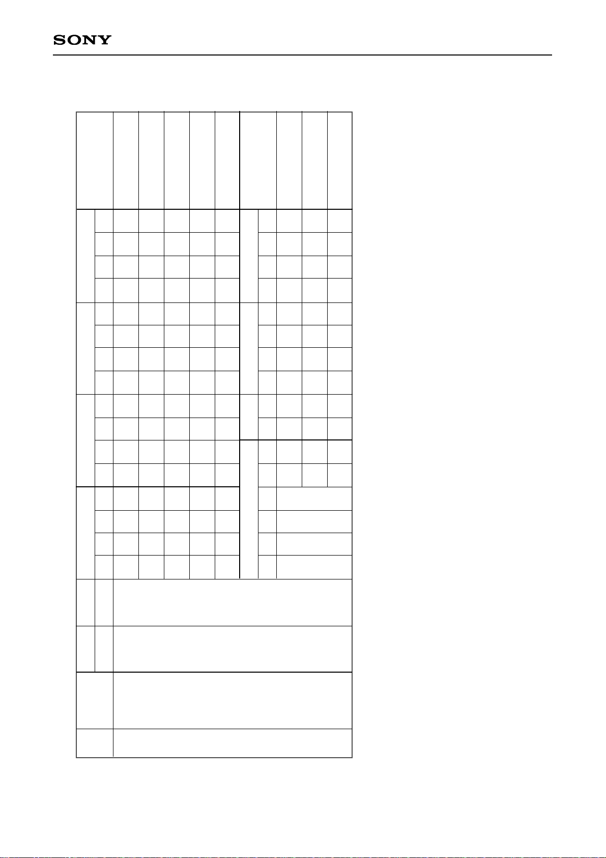
– 24 –
CXD3029R
Regis-
ter
Command Table ($348X to 3FX)
PGFS, PFOK, RFAC
DOUT
Booster Surf Brake
Booster
DFCT
FCS Bias Limit
FCS Bias Data
Traverse Center Data
3
1
1
1
1
1
1
0
0
0
1
1
1
0
1
1
0
1
1
0
0
1
0
0
1
PGFS1
A/D
SEL
SFBK1
THBON
IDFS3
1
0
0
PGFS0
COPY
EN
SFBK2
FHBON
IDFS2
0
1
0
PFOK1
EMPH
D
0
TLB10N
IDFS1
FBL9
FB9
TV9
PFOK0
CAT
b8
0
FLB1ON
IDFS0
FBL8
FB8
TV8
0
DOUT
EN1
LB1
SN
TLB2ON
0
FBL7
FB7
TV7
0
DOUT
DMUT
LB2
SN
0
DF
SLS
FBL6
FB6
TV6
0
DOUT
WOD
LB2
SM
HBST1
IDFT1
FBL5
FB5
TV5
MRS
WIN
EN
0
HBST0
IDFT0
FBL4
FB4
TV4
MRT1
DOUT
EN2
0
LB1S1
0
FBL3
FB3
TV3
MRT0
0
0
LB1S0
0
FBL2
FB2
TV2
0
0
0
LB2S1
LPDF
0
FBL1
FB1
TV1
0
0
0
LB2S0
INVRFDC
—
—
TV0
SELECT
Command
Address 1 Address 2
D23 to D20
Address 3
D15
D15 D14 D13 D12 D11 D10 D9 D8 D7 D6 D5 D4 D1 D0D3 D2
Data 3Data 2Data 1Address 3
D14 D13 D12
Data 1
D11 D10 D9 D8
Data 2
D7 D6 D5 D4
Data 3
D3 D2 D1 D0
0 0 1 1
D19 to D16
0 1 0 0
Page 25
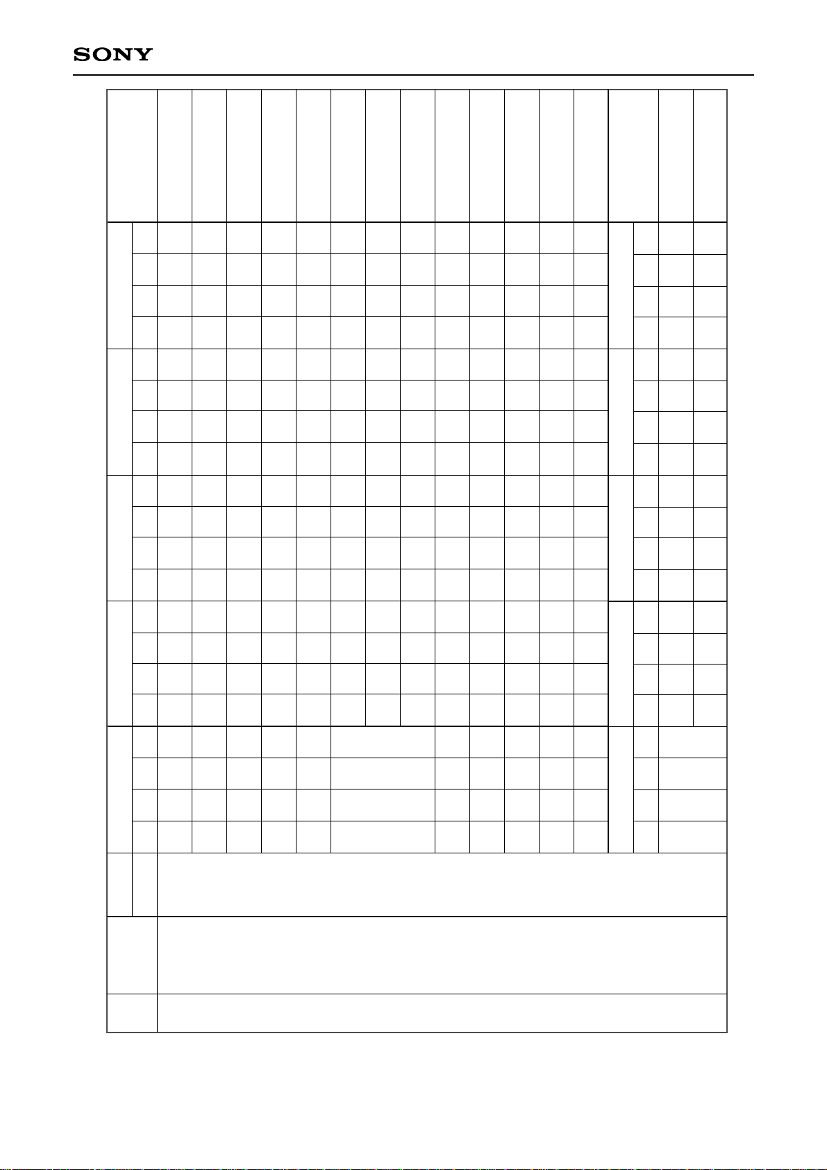
– 25 –
CXD3029R
FCS search, AGF
TRK jump, AGT
FZC, AGC, SLD move
DC measure, cancel
Serial data readout
FCS Bias, Gain,
Surf jump/brake
Gain
FOCUS
Mirr, DFCT, FOK
TZC, COUT, Bottom,
MIRR
SLD filter
Filter
Clock, others
3
FT1
TDZC
FZSH
VCLM
DAC
0
1
1
SFO2
COSS
SFID
F1NM
0
1
0
1
0
1
0
1
0
1
0
1
0
1
1
0
0
1
1
0
0
1
1
1
1
1
0
0
0
0
1
1
1
1
0
0
0
1
1
1
1
1
1
1
1
FT0
DTZC
FZSL
VCLC
SD6
FBON
0
0
SFO1
COTS
SFSK
F1DM
AGG4
FS5
TJ5
SM5
FLM
SD5
FBSS
0
0
SDF2
CETZ
THID
F3NM
XT4D
FS4
TJ4
SM4
FLC0
SD4
FBUP
0
1
SDF1
CETF
THSK
F3UM
XT2D
FS3
TJ3
SM3
RFLM
SD3
FBV1
FPG
S1
0
MAX2
COT2
ABEF
T1NM
0
FS2
TJ2
SM2
RFLC
SD2
FBV0
FPG
S0
0
MAX1
COT1
TLD2
T1UM
DRR2
FS1
TJ1
SM1
AGF
SD1
FIF
ZC
TPG
S1
0
SFOX
MOT2
TLD1
T3NM
DRR1
FS0
TJ0
SM0
AGT
SD0
TJD0
TPG
S0
0
BTF
0
TLD0
T3DM
DRR0
FTZ
SFJP
AGS
DFSW
0
FPS1
0
UD
FZC
D2V2
BTS1
SDF6
DFIS
0
FG6
TG6
AGJ
LKSW
0
FPS0
0
0
D2V1
BTS0
SDF5
TLCD
ASFG
FG5
TG5
AGGF
TBLM
0
TPS1
0
0
D1V2
MRC1
SDF4
0
FTQ
FG4
TG4
AGGT
TCLM
0
TPS0
0
0
D1V1
MRC0
SDF3
LKIN
1
FG3
TG3
AGV1
FLC1
0
SVDA
0
0
RINT
0
0
COIN
SRO1
FG2
TG2
AGV2
TLC2
0
SJHD
0
0
0
0
0
MDFI
0
FG1
TG1
AGHS
TLC1
0
INBK
0
0
0
0
0
MIRI
AGHF
FG0
TG0
AGHT
TLC0
0
MTI0
0
0
0
0
0
XT1D
ASOT
SELECT
Regis-
ter
Command
Address 1 Address 2
D23 to D20 D19 D18 D17 D16
Data 1
D15 D14 D13 D12
Data 2
D11 D10 D9 D8
Data 3
D7 D6 D5 D4
Data 4
D3 D2 D1 D0
0 0 1 1
Command Table ($34FX to 3FX) cont.
System GAIN
FOCUS
1
1
0
0
0
0
0
1
SYG3
FSUD
SYG2
FFS
UP
SYG1
0
SYG0
1
FI
FZB3
0
FI
FZB2
0
FI
FZB1
FFS5
FI
FZB0
FFS4
FI
FZA3
FFS3
FI
FZA2
FFS2
FI
FZA1
FFS1
FI
FZA0
FFS0
Address 2
D19 D18 D17 D16
Address 3
D15 D14 D13 D12
Data 1
D11 D10 D9 D8
Data 2
D7 D6 D5 D4
Data 3
D3 D2 D1 D0
1
111
Page 26
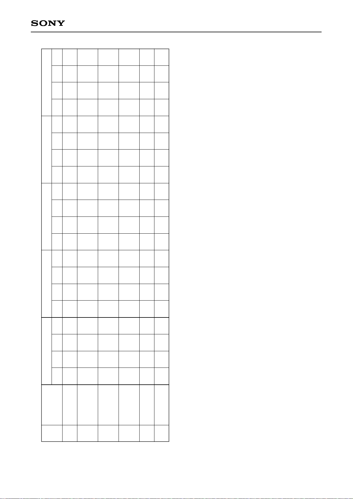
– 26 –
CXD3029R
Command Table ($4X to EX)
—: don’t care
Auto sequence
Blind (A, E),
Brake (B),
Overflow (C, G)
Sled KICK,
BRAKE (D),
KICK (F)
Auto sequence (N)
track jump count
setting
MODE
specification
Function
specification
0
0
0
0
1
1
1
1
1
1
0
0
0
0
1
1
0
0
0
1
0
1
0
1
AS3
TR3
SD3
32768
CD-
ROM
1
AS2
TR2
SD2
16384
DOUT
Mute
DSPB
ON-OFF
AS1
TR1
SD1
8192
DOUT
Mute-F
ASEQ
ON-OFF
AS0
TR0
SD0
4096
WSEL
1
MT3
0
KF3
2048
VCO
SEL2
BiliGL
MAIN
MT2
0
KF2
1024
ASHS
BiliGL
SUB
MT1
0
KF1
512
SOCT0
FLFC
MT0
0
KF0
256
VCO
SEL1
0
LSSL
0
0
128
KSL3
0
0
0
0
64
KSL2
0
0
0
0
32
KSL1
0
0
0
0
16
KSL0
0
—
—
—
8
VCO1
CS1
1
—
—
—
4
VCO1
CS0
0
—
—
—
2
0
0
—
—
—
1
0
1
4
5
6
7
8
9
Regis-
ter
Command
Address
D3 D2 D1 D0 D3 D2 D1 D0 D3 D2 D1 D0 D3 D2 D1 D0 D3 D2 D1 D0
Data 1 Data 2 Data 3 Data 4
Page 27
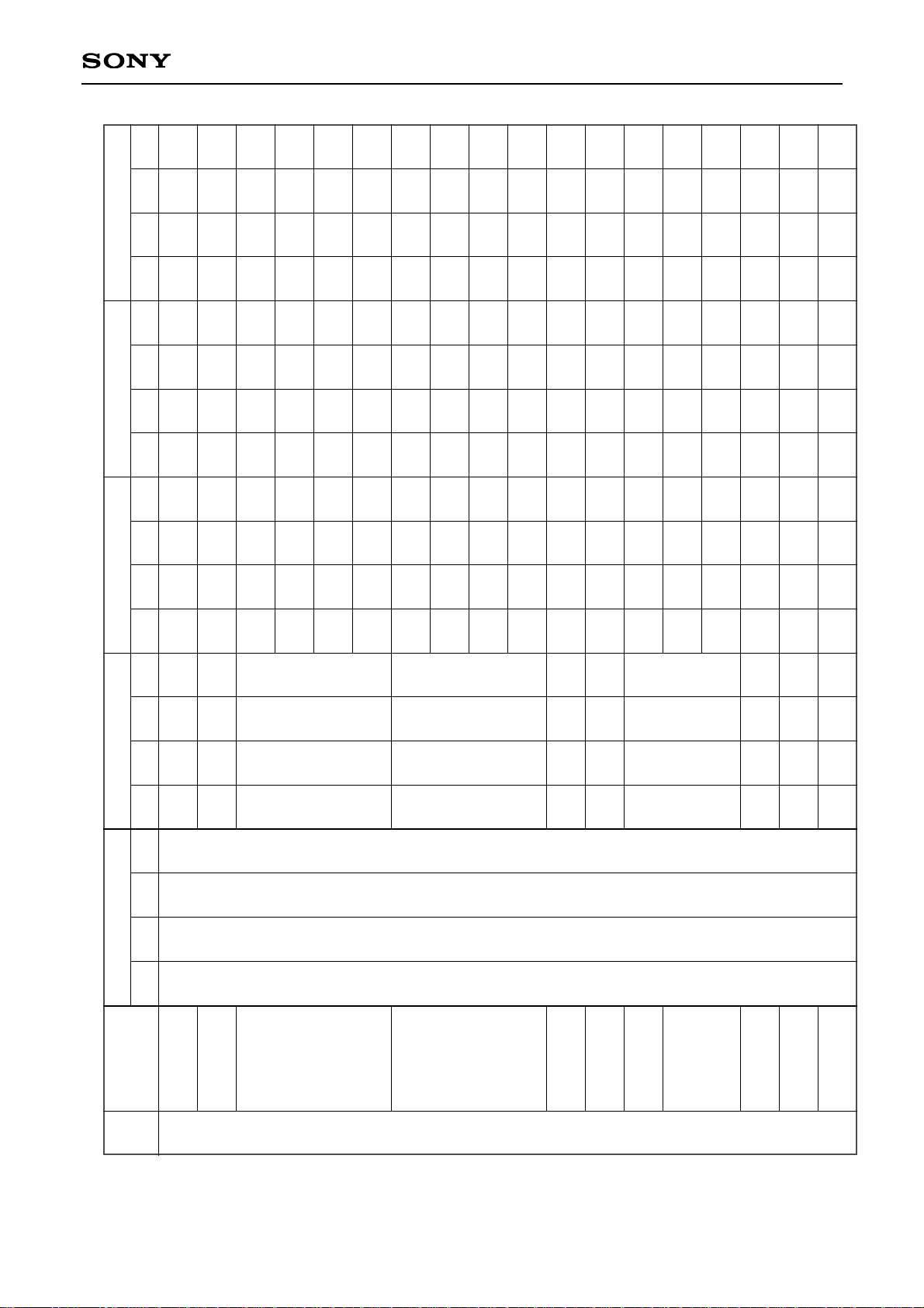
– 27 –
CXD3029R
Command Table ($4X to EX) cont.
Audio CTRL
Signal select
Bass boost
Headphone
Shock-proof
memory setting
Shock-proof
memory control
DOUT subcode-Q
setting
DRAM I/F
Compression
setting
EFM playability
enhancement settin
g
Sync expansion
specification
101
0
0
0
0
0
0
1
1
1
1
1
0
1
1
1
1
0
0
0
0
1
Mute
0
0
1
1
0
0
1
1
0
ATT
0
1
0
1
0
1
0
1
0
PCT1
RSL1
0
0
1
1
0
0
1
1
SL
XQOK
XQOK
SubQA3
1
1
ADPON
ARDTEN
AVW
PCT2
RSL0
0
1
0
1
0
1
0
1
SL
XWRE
XWRE
SubQA2
1
1
BITSL1
1
0
0
0
1
PWDN
BBON1
COMP
ON
1
PWDN
BBON1
COMP
ON
GTOP
CHECK
XRDE
SubQA1
1
1
BITSL0
1
SFP5
SOC2
0
ZMUTA
ZDPL
BBON0
0
ZMUTA
ZDPL
BBON0
0
NOLIM
WDCK
XSOEO
SubQA0
0
1
0
1
SFP4
0
DTSL1
SMUT
WOC
HBON1
0
SMUT
XWOC
HBON1
0
SPSL
COM
XSOEO2
0
1
DADR19
ADP
WO
1
SFP3
0
DTSL0
AD10
DAC
EMPH
HBON0
0
AD10
DAC
EMPH
HBON0
0
READ2
ADDRST
0
DRWR
DADR18
0
0
SFP2
0
MCSL1
AD9
HiCut
FILTER
BBSL1
0
AD9
HiCut
FILTER
BBSL1
0
REFSEL
SCOR
MOD
0
DRADR
DADR17
0
1
SFP1
0
MCSL0
AD8
BST
CL
BBSL0
0
AD8
BST
CL
BBSL0
0
REFON
SDTO
OUT
0
0
DADR16
0
0
SFP0
0
0
AD7
1
HBSL1
0
AD7
1
HBSL1
0
XOE
OUT
SubQD7
DRD15
DADR15
0
0
0
1
SDSL2
AD6
0
HBSL0
0
AD6
0
HBSL0
0
MSL2
SubQD6
DRD14
DADR14
GRSEL
0
0
0
SDSL1
AD5
OBIT1
BBST
Vdwn1
1
AD5
OBIT1
BBST
Vdwn1
1
MSL1
SubQD5
DRD13
DADR13
0
1
0
0
SDSL0
AD4
OBIT0
BBST
Vdwn0
0
AD4
OBIT0
BBST
Vdwn0
0
MSL0
SubQD4
DRD12
DADR12
0
0
0
A
Regis-
ter
Command
Address
D3 D2 D1 D0 D3 D2 D1 D0 D3 D2 D1 D0 D3 D2 D1 D0 D3 D2 D1 D0
Data 1 Data 2 Data 3 Data 4
Page 28
– 28 –
CXD3029R
Command Table ($4X to EX) cont.
1
1
1
1
0
1
1
1
1
0
0
1
1
0
1
0
1010
1
1
1
32768
Gain
MDP1
0
CM3
Sleep setting
Variable pitch
setting
Spindle servo
setting
Traverse monitor
counter setting
Spindle servo
coefficient setting
CLV CTRL
SPD mode
1
1
1
16384
Gain
MDP0
TB
CM2
0
1
1
8192
Gain
MDS1
TP
CM1
1
0
1
4096
Gain
MDS0
Gain
CLVS
CM0
ADCPS
VARI
ON
SYG3
EA
2048
Gain
DCLV1
VP7
EPWM
DSP
SLEEP
VARI
USE
SYG2
EA
1024
Gain
DCLV0
VP6
SPD
DSSP
SLEEP
WTC
C2PO
SYG1
EA
512
PCC1
VP5
ICAP
ASYM
SLEEP
SCSY
(sub)
SYG0
EA
256
PCC0
VP4
SFSL
ESP
SLEEP
SENS
SEL3
MDP
OUTSL1
128
SFP3
VP3
VC2C
LPF
SLEEP
SENS
SEL2
MDP
OUTSL0
64
SFP2
VP2
HIFC
DSUB
SLEEP
SENS
SEL1
LPWR2
32
SFP1
VP1
LPWR
ASEQ
SLEEP
SENS
SEL0
0
16
SFP0
VP0
VPON
PCOL
MDS
CTL
8
SRP3
VP
CTL1
Gain
CAV1
HCAV
SLEEP
MDP
UP
4
SRP2
VP
CTL0
Gain
CAV0
0
0
2
SPR1
0
0
0
MDP
CTL4
1
SRP0
0
INV
VPCO
B
C
D
E
A
Regis-
ter
Command
Address
D3 D2 D1 D0 D3 D2 D1 D0 D3 D2 D1 D0 D3 D2 D1 D0 D3 D2 D1 D0
Data 1 Data 2 Data 3 Data 4
Page 29
– 29 –
CXD3029R
—: don’t care
Command Table ($4X to EX) cont.
MODE
specification
Function
specification
AUDIO CTRL
Signal select
Bass boost
Headphone
Shock-proof
memory setting
DOUT subcode-Q
setting
DRAM I/F
Compression
setting
8
9
A
1 0 0 0
1 0 0 1
1 0 1 0
0 0 ∗ ∗
0 1 0 0
0 1 0 1
0 1 1 0
0 1 1 1
1 0 0 1
1 0 1 0
0 0 1 ∗
0 1 ∗ ∗
1 0 ∗ ∗
1 1 ∗ 0
001∗
01∗ ∗
10∗ ∗
11∗ 0
∗∗∗∗
1 1 1 0
1 1 1 1
0 0 0 0
ERC4
0
0
EN
XSOE
AD3
0
BBST
Vup1
0
AD3
0
BBST
Vup1
0
ADDRST
SEL
SubQD3
DRD11
DADR11
ADPCM
SEL
SCOR
SEL
0
0
CKOUT
SL2
AD2
1
BBST
Vup0
0
AD2
1
BBST
Vup0
0
ADRMO
SubQD2
DRD10
DADR10
ADPCM
MUTE
SCSY
0
0
CKOUT
SL1
AD1
0
BBST
Uth
0
AD1
0
BBST
Uth
0
GRSCOR
MOD
SubQD1
DRD9
DADR9
0
SOCT1
0
0
SLD
BBIN
AD0
0
BBST
Lth
PDM
INV
AD0
0
BBST
Lth
PDM
INV
STA
SEL
SubQD0
DRD8
DADR8
0
TXON
0
0
max
C2PO7
XWI
H2
DRD7
DADR7
MLAT
TXOUT
0
0
max
C2PO6
XWI
H1
DRD6
DADR6
ORMU
OUTL1
0
0
max
C2PO5
SPSL
COM
DRD5
DADR5
0
OUTL0
0
0
max
C2PO4
WQR
MON
DRD4
DADR4
0
0
DIV4
—
max
C2PO3
A11
SEL
DRD3
DADR3
0
0
—
max
C2PO2
READ
S2
DRD2
DADR2
OUTL2
0
—
max
C2PO1
READ
S1
DRD1
DADR1
0
0
—
max
C2PO0
MON
SEL
DRD0
DADR0
Regis-
ter
Command
Address Data 1 Data 2 Data 3 Data 4
D3 D2 D1 D0 D3 D2 D1 D0 D3 D2 D1 D0
Data 5 Data 6 Data 7
Page 30
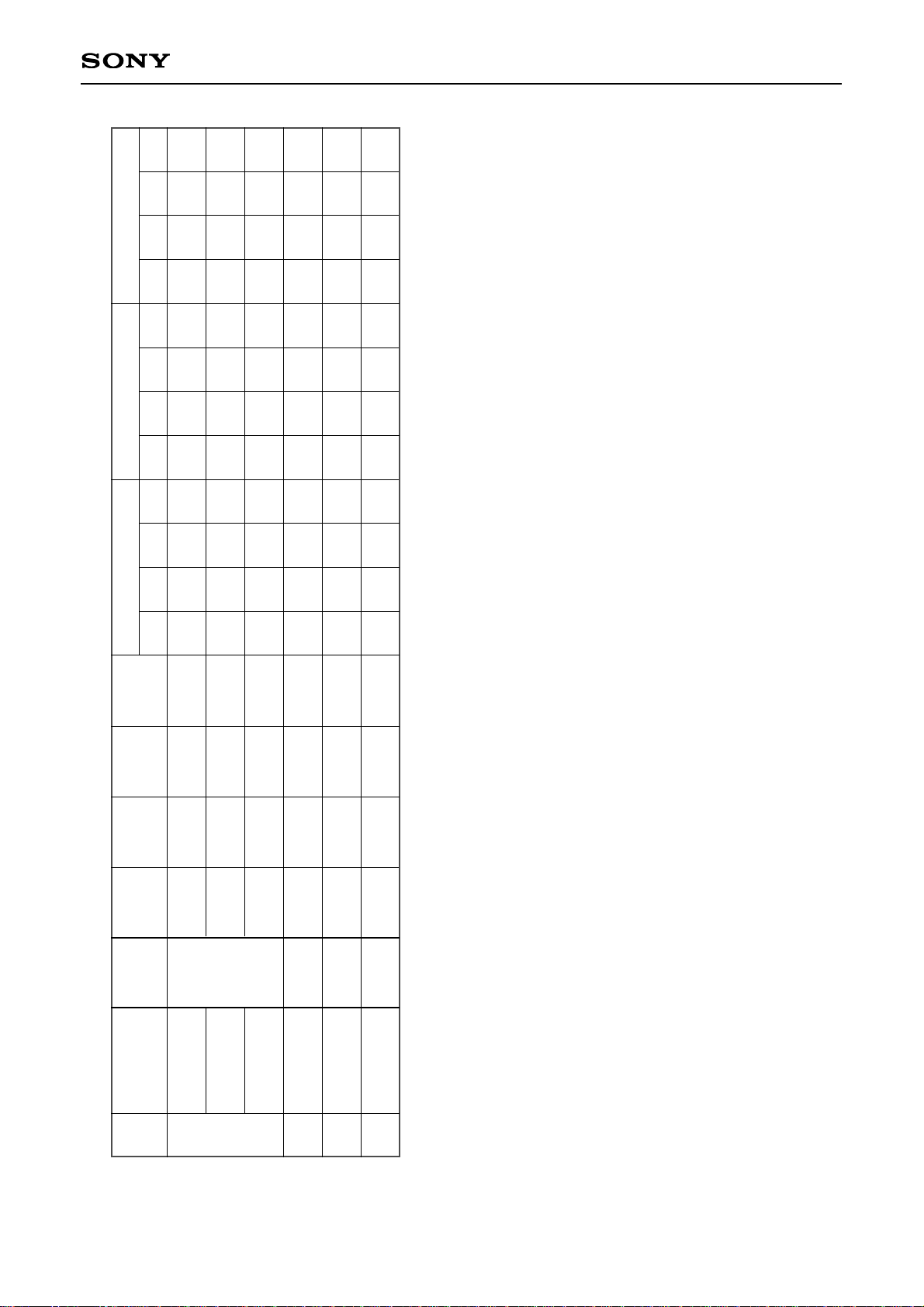
– 30 –
CXD3029R
—: don’t care
Command Table ($4X to EX) cont.
EFM playability
enhancement setting
Sync expansion
specification
Spindle servo
setting
Traverse monitor
counter setting
Spindle servo
coefficient setting
CLV CTRL
A
B
C
D
1 0 1 0
1 0 1 1
1 1 0 0
1 1 0 1
1 0 1 1
1 1 0 0
1 1 1 1
1
REF
SEL2
MDP
CTL3
0
EDC7
0
0
SLIM1
MDP
CTL2
0
EDC6
0
0
SLIM0
MDP
CTL1
MTSL1
EDC5
0
0
OV4
MDP
CTL0
MTSL0
EDC4
0
0
OV3
ASYE
EDC3
0
0
OV2
MD2
EDC2
0
0
OV1
0
EDC1
0
0
OV0
0
EDC0
0
1
—
—
0
—
—
0
—
—
0
—
—
Regis-
ter
Command
Address Data 1 Data 2 Data 3 Data 4
D3 D2 D1 D0 D3 D2 D1 D0 D3 D2 D1 D0
Data 5 Data 6 Data 7
Page 31

– 31 –
CXD3029R
FOCUS SERVO OFF,
0V OUT
TRACKING GAIN UP
FILTER SELECT 1
TRACKING SERVO OFF
SLED SERVO OFF
SLED KICK LEVEL
(±1 × basic value) (default)
KRAM DATA
($3400XX to $344FXX)
0
0
0
0
0
0
0
0
0
0
1
0
—
—
—
—
—
—
—
—
—
—
—
—
—
—
—
—
—
—
—
—
—
—
—
—
—
—
—
—
—
—
—
—
—
—
—
—
—
—
—
—
—
—
—
—
—
—
—
—
0
1
2
0 0 0 0
0 0 0 1
0 0 1 0
FOCUS
CONTROL
TRACKING
CONTROL
TRACKING
MODE
Regis-
ter
Command
Address
D23 to D20
Data 1
D19 D18 D17 D16
Data 2
D15 D14 D13 D12
Data 3
D11 D10 D9 D8
Data 4
D7 D6 D5 D4
Data 5
D3 D2 D1 D0
Regis-
ter
Command
3 SELECT
Address
D23 to D20
0 0 1 1
0 0 1 1 0 1 0 0 0 See "Coefficient ROM Preset Values Table".
0000————————————————
Data 1
D19 D18 D17 D16
Data 2
D15 D14 D13 D12
Data 3
D11 D10 D9
Data 4
D7 D6 D5 D4
Data 5
D3 D2 D0 D0
Address 1
D23 to D20 D19 D18 D17 D16
Address 2
D15 D14 D13 D12
Address 3
D11 D10 D9 D8
Data 1
D7 D6 D5 D4
Data 2
D3 D2 D0 D0
§1-3. CPU Command Presets
Command Preset Table ($0X to 34X)
—: don’t care
Page 32

– 32 –
CXD3029R
Command Preset Table ($348X to 34FX)
PGFS, PFOK, RFAC
CAV control
DOUT
Booster Surf Brake
Booster
Servo DAC output
DFCT
FCS Bias Limit
FCS Bias Data
Traverse Center Data
3
1
1
1
1
1
1
1
1
0
0
0
0
1
1
1
1
0
0
1
1
0
0
1
1
0
1
0
1
0
1
0
1
0
0
0
0
0
0
0
1
0
0
0
0
0
0
0
0
0
0
1
0
0
0
0
0
0
0
0
0
0
0
0
0
1
0
0
0
0
0
0
0
0
0
0
0
0
0
0
0
0
0
0
0
1
0
0
0
0
0
0
0
0
0
0
0
0
0
0
0
0
0
0
0
1
0
0
0
0
0
0
0
0
0
0
0
0
0
0
0
0
0
0
0
0
0
0
0
0
0
0
0
0
0
0
0
0
0
0
0
0
0
0
0
0
0
0
0
0
—
—
0
SELECT
Regis-
ter
Command
Address 1 Address 2
D23 to D20
Address 3
D15
D15 D14 D13 D12
D11
D10 D9 D8 D7 D6 D5 D4 D1 D0D3 D2
Data 3Data 2Data 1Address 3
D14 D13 D12
Data 1
D11 D10 D9 D8
Data 2
D7 D6 D5 D4
Data 3
D3 D2 D1 D0
0 0 1 1
D19 to D16
0 1 0 0
—: don’t care
Page 33

– 33 –
CXD3029R
Command Preset Table ($34FX to 3FX) cont.
FCS search, AGF
TRK jump, AGT
FZC, AGC, SLD move
DC measure, cancel
Serial data read out
FCS Bias, Gain,
Surf jump/brake
Gain
FOCUS
MIRR, DFCT, FOK
TZC, COUT, Bottom,
MIRR
SLD filter
Filter
Clock, others
3
0
0
0
0
0
0
1
1
1
0
0
0
0
1
0
1
0
1
0
1
0
1
0
1
0
1
1
0
0
1
1
0
0
1
1
1
1
1
0
0
0
0
1
1
1
1
0
0
0
1
1
1
1
1
1
1
1
1
0
1
0
0
0
0
0
1
0
0
0
0
0
0
0
0
0
0
0
0
1
0
0
0
0
1
0
1
0
0
0
0
1
0
0
0
0
0
1
1
0
0
0
0
0
0
0
0
0
0
0
0
1
0
0
0
0
0
0
0
0
0
0
0
0
1
0
0
0
0
0
0
0
0
0
0
0
0
0
0
0
0
0
0
0
0
0
0
0
0
0
0
1
0
0
0
0
0
0
1
0
0
0
0
0
0
0
0
0
0
0
1
0
0
0
0
1
1
1
0
0
0
0
0
0
0
0
0
0
0
0
1
0
0
0
0
0
1
0
0
0
1
1
1
0
0
0
0
0
0
0
0
0
0
0
1
1
0
0
0
0
0
0
0
0
0
0
0
0
1
1
0
0
0
0
0
0
0
0
0
0
1
0
0
0
0
0
0
0
0
0
0
0
0
SELECT
Regis-
ter
Command
Address 1 Address 2
D23 to D20
D19 D18 D17 D16
Data 1
D15 D14 D13 D12
Data 2
D11 D10 D9 D8
Data 3
D7 D6 D5 D4
Data 4
D3 D2 D1 D0
0 0 1 1
System GAIN
FOCUS
1
1
0
0
0
0
0
1
1
0
0
0
0
0
0
0
0
0
0
0
0
0
0
0
0
0
0
0
0
0
0
0
Address 2
D19 D18 D17 D16
Address 3
D15 D14 D13 D12
Data 1
D11 D10 D9 D8
Data 2
D7 D6 D5 D4
Data 3
D3 D2 D1 D0
1
111
Page 34

– 34 –
CXD3029R
Auto sequence
Blind (A, E),
Brake (B),
Overflow (C, G)
Sled KICK,
BRAKE (D),
KICK (F)
Auto sequence (N)
track jump count
setting
MODE setting
Function
specification
4
5
6
7
8
9
Regis-
ter
Command
Address
D3 D2 D1 D0 D3 D2 D1 D0 D3 D2 D1 D0 D3 D2 D1 D0 D3 D2 D1 D0
Data 1 Data 2 Data 3 Data 4
Command Preset Table ($4X to EX)
—: don’t care
0
0
0
0
1
1
1
1
1
1
0
0
0
0
1
1
0
0
0
1
0
1
0
1
0
0
0
0
0
1
0
1
1
0
0
0
0
0
1
0
0
0
0
1
1
0
0
1
0
0
0
0
0
0
0
0
0
0
0
0
0
0
0
0
0
0
0
0
0
1
0
1
0
0
0
0
0
0
0
0
0
0
0
0
0
0
0
0
1
0
0
0
0
0
0
0
—
—
—
0
0
1
—
—
—
0
0
0
—
—
—
0
0
0
—
—
—
0
0
1
Page 35

– 35 –
CXD3029R
Audio CTRL
Signal select
Bass boost
Headphone
Shock-proof
memory setting
Shock-proof
memory control
DOUT subcode-Q
setting
DRAM I/F
Compression
setting
EFM playability
enhancement setting
Sync expansion
specification
101
0
A
Regis-
ter
Command
Address
D3 D2 D1 D0 D3 D2 D1 D0 D3 D2 D1 D0 D3 D2 D1 D0 D3 D2 D1 D0
Data 1 Data 2 Data 3 Data 4
Command Preset Table ($4X to EX) cont.
0
0
0
0
0
1
1
1
1
1
0
1
1
1
1
0
0
0
0
1
1
0
0
1
1
0
0
1
1
0
1
0
1
0
1
0
1
0
1
0
0
1
0
0
1
1
0
0
1
1
0
1
0
1
1
0
0
0
0
0
0
1
0
1
0
1
0
1
0
1
0
1
1
0
1
0
0
0
1
0
0
0
1
0
0
0
1
1
0
1
1
0
1
0
0
0
0
0
0
0
0
0
0
0
0
1
0
0
1
0
1
0
0
1
0
0
0
0
0
0
0
0
0
1
0
1
0
0
1
1
0
0
1
0
0
0
1
0
0
0
0
0
0
0
0
0
0
1
0
0
0
0
0
0
0
0
0
0
0
0
0
0
0
0
1
0
0
0
0
0
0
0
0
0
0
0
0
0
0
0
0
0
0
0
0
0
0
1
0
0
0
1
0
0
0
0
0
0
0
0
0
1
0
0
0
0
0
0
0
0
0
0
0
0
0
1
0
0
0
0
0
1
0
1
0
1
0
1
0
0
0
0
0
1
0
0
0
0
0
0
0
0
0
0
0
0
0
0
0
0
0
0
Page 36

– 36 –
CXD3029R
1
1
1
1
0
1
1
1
1
0
0
1
1
0
1
0
1010
Sleep setting
Variable pitch
setting
Spindle servo
setting
Traverse monitor
counter setting
Spindle servo
coefficient setting
CLV CTRL
SPD mode
B
C
D
E
A
Regis-
ter
Command
Address
D3 D2 D1 D0 D3 D2 D1 D0 D3 D2 D1 D0 D3 D2 D1 D0 D3 D2 D1 D0
Data 1 Data 2 Data 3 Data 4
Command Preset Table ($4X to EX) cont.
1
1
1
0
0
0
0
1
1
1
0
0
0
0
0
1
1
0
0
0
0
1
0
1
0
0
0
0
0
0
1
0
0
0
0
0
0
0
0
0
0
0
0
0
0
0
0
0
0
0
0
0
1
0
0
0
0
0
0
0
1
0
0
1
0
0
0
1
0
0
0
0
0
0
0
0
0
0
0
0
0
0
0
0
0
0
0
0
0
0
0
0
0
0
0
0
1
0
0
0
0
1
0
0
Page 37

– 37 –
CXD3029R
—: don’t care
MODE
specification
Function
specification
AUDIO CTRL
Signal select
Bass boost
Headphone
Shock-proof
memory setting
DOUT subcode-Q
setting
DRAM I/F
Compression
setting
8
9
A
1 0 0 0
1 0 0 1
1 0 1 0
Regis-
ter
Command
Address Data 1 Data 2 Data 3 Data 4
D3 D2 D1 D0 D3 D2 D1 D0 D3 D2 D1 D0
Data 5 Data 6 Data 7
Command Preset Table ($4X to EX) cont.
0 0 ∗ ∗
0 1 0 0
0 1 0 1
0 1 1 0
0 1 1 1
1 0 0 1
1 0 1 0
0 0 1 ∗
0 1 ∗ ∗
1 0 ∗ ∗
1 1 ∗ 0
0 0 1 ∗
01∗ ∗
10∗ ∗
11∗ 0
∗∗∗∗
1 1 1 0
1 1 1 1
0 0 0 0
0
0
0
0
0
0
0
0
0
0
0
0
0
0
0
0
0
0
0
0
0
0
1
0
0
0
1
0
0
0
0
0
0
0
0
0
0
0
0
0
0
0
0
0
0
0
0
0
0
0
0
0
0
0
0
0
0
0
0
0
0
0
0
0
0
0
0
0
0
0
0
0
0
0
0
0
0
0
0
0
0
0
0
1
0
0
0
0
0
0
0
0
0
0
0
0
0
0
0
0
0
0
—
0
0
0
0
0
0
—
0
0
0
0
0
0
—
0
0
0
0
0
0
—
0
0
0
0
Page 38

– 38 –
CXD3029R
—: don’t care
Command Preset Table ($4X to EX) cont.
EFM playability
enhancement setting
Sync expansion
specification
Spindle servo
setting
Traverse monitor
counter setting
Spindle servo
coefficient setting
CLV CTRL
A
B
C
D
1 0 1 0
1 0 1 1
1 1 0 0
1 1 0 1
1 0 1 1
1 1 0 0
1 1 1 1
1
1
0
0
0
0
0
0
0
0
0
0
0
0
0
0
0
0
0
0
0
0
0
0
0
0
0
1
0
0
0
0
0
0
0
0
0
0
0
0
0
0
0
1
1
0
0
0
1
—
—
0
—
—
0
—
—
0
—
—
Regis-
ter
Command
Address Data 1 Data 2 Data 3 Data 4
D3 D2 D1 D0 D3 D2 D1 D0 D3 D2 D1 D0
Data 5 Data 6 Data 7
Page 39

– 39 –
CXD3029R
∗
Fix indicates that normal preset values should be used.
(Coefficient ROM Preset Values Table (1))
ADDRESS
K00
K01
K02
K03
K04
K05
K06
K07
K08
K09
K0A
K0B
K0C
K0D
K0E
K0F
E0
81
23
7F
6A
10
14
30
7F
46
81
1C
7F
58
82
7F
SLED INPUT GAIN
SLED LOW BOOST FILTER A-H
SLED LOW BOOST FILTER A-L
SLED LOW BOOST FILTER B-H
SLED LOW BOOST FILTER B-L
SLED OUTPUT GAIN
FOCUS INPUT GAIN
SLED AUTO GAIN
FOCUS HIGH CUT FILTER A
FOCUS HIGH CUT FILTER B
FOCUS LOW BOOST FILTER A-H
FOCUS LOW BOOST FILTER A-L
FOCUS LOW BOOST FILTER B-H
FOCUS LOW BOOST FILTER B-L
FOCUS PHASE COMPENSATE FILTER A
FOCUS DEFECT HOLD GAIN
K10
K11
K12
K13
K14
K15
K16
K17
K18
K19
K1A
K1B
K1C
K1D
K1E
K1F
K20
K21
K22
K23
K24
K25
K26
K27
K28
K29
K2A
K2B
K2C
K2D
K2E
K2F
4E
32
20
30
80
77
80
77
00
F1
7F
3B
81
44
7F
5E
FOCUS PHASE COMPENSATE FILTER B
FOCUS OUTPUT GAIN
ANTI SHOCK INPUT GAIN
FOCUS AUTO GAIN
HPTZC / Auto Gain HIGH PASS FILTER A
HPTZC / Auto Gain HIGH PASS FILTER B
ANTI SHOCK HIGH PASS FILTER A
HPTZC / Auto Gain LOW PASS FILTER B
Fix
∗
TRACKING INPUT GAIN
TRACKING HIGH CUT FILTER A
TRACKING HIGH CUT FILTER B
TRACKING LOW BOOST FILTER A-H
TRACKING LOW BOOST FILTER A-L
TRACKING LOW BOOST FILTER B-H
TRACKING LOW BOOST FILTER B-L
82
44
18
30
7F
46
81
3A
7F
66
82
44
4E
1B
00
00
TRACKING PHASE COMPENSATE FILTER A
TRACKING PHASE COMPENSATE FILTER B
TRACKING OUTPUT GAIN
TRACKING AUTO GAIN
FOCUS GAIN DOWN HIGH CUT FILTER A
FOCUS GAIN DOWN HIGH CUT FILTER B
FOCUS GAIN DOWN LOW BOOST FILTER A-H
FOCUS GAIN DOWN LOW BOOST FILTER A-L
FOCUS GAIN DOWN LOW BOOST FILTER B-H
FOCUS GAIN DOWN LOW BOOST FILTER B-L
FOCUS GAIN DOWN PHASE COMPENSATE FILTER A
FOCUS GAIN DOWN DEFECT HOLD GAIN
FOCUS GAIN DOWN PHASE COMPENSATE FILTER B
FOCUS GAIN DOWN OUTPUT GAIN
Not used
Not used
DATA CONTENTS
Page 40

– 40 –
CXD3029R
<Coefficient ROM Preset Values Table (2)>
ADDRESS
K30
K31
K32
K33
K34
K35
K36
K37
K38
K39
K3A
K3B
K3C
K3D
K3E
K3F
80
66
00
7F
6E
20
7F
3B
80
44
7F
77
86
0D
57
00
SLED INPUT GAIN (Only when TRK gain up2 is accessed with SFSK = 1.)
ANTI SHOCK LOW PASS FILTER B
Not used
ANTI SHOCK HIGH PASS FILTER B-H
ANTI SHOCK HIGH PASS FILTER B-L
ANTI SHOCK FILTER COMPARATE GAIN
TRACKING GAIN UP2 HIGH CUT FILTER A
TRACKING GAIN UP2 HIGH CUT FILTER B
TRACKING GAIN UP2 LOW BOOST FILTER A-H
TRACKING GAIN UP2 LOW BOOST FILTER A-L
TRACKING GAIN UP2 LOW BOOST FILTER B-H
TRACKING GAIN UP2 LOW BOOST FILTER B-L
TRACKING GAIN UP PHASE COMPENSATE FILTER A
TRACKING GAIN UP PHASE COMPENSATE FILTER B
TRACKING GAIN UP OUTPUT GAIN
Not used
K40
K41
K42
K43
K44
K45
K46
K47
K48
K49
K4A
K4B
K4C
K4D
K4E
K4F
04
7F
7F
79
17
6D
00
00
02
7F
7F
79
17
54
00
00
TRACKING HOLD FILTER INPUT GAIN
TRACKING HOLD FILTER A-H
TRACKING HOLD FILTER A-L
TRACKING HOLD FILTER B-H
TRACKING HOLD FILTER B-L
TRACKING HOLD FILTER OUTPUT GAIN
TRACKING HOLD FILTER INPUT GAIN
(Only when TRK gain up2 is accessed with THSK = 1.)
Not used
FOCUS HOLD FILTER INPUT GAIN
FOCUS HOLD FILTER A-H
FOCUS HOLD FILTER A-L
FOCUS HOLD FILTER B-H
FOCUS HOLD FILTER B-L
FOCUS HOLD FILTER OUTPUT GAIN
Not used
Not used
DATA CONTENTS
Page 41

– 41 –
CXD3029R
§1-4. Description of SENS Signals
SENS output
Microcomputer
serial register
(latching not required)
$0X
$1X
$2X
$30 to 37
$38
$38
$39X
$3A
$3B to 3F
$4X
$5X
$6X
$A0 to $A8
$AA to $AF
$BX
$CX
$EX
$7X, 8X, 9X,
DX, FX
Z
Z
Z
Z
Z
Z
Z
Z
Z
Z
Z
Z
GFS
COMP
COUT
OV64
Z
FZC
AS
TZC
SSTP
AGOK
∗
XAVEBSY
∗
See the table on page 174.
FBIAS Count STOP
SSTP
XBUSY
FOK
0
GFS
COMP
COUT
OV64
0
—
—
—
—
—
—
8 to 16 bits
—
—
—
—
—
—
—
—
—
—
ASEQ = 0 ASEQ = 1 Output data length
∗
$38 outputs AGOK during AGT and AGF command settings, and XAVEBSY during AVRG measurement.
SSTP is output in all other cases.
Page 42

– 42 –
CXD3029R
Description of SENS Signals
The SENS pin is high impedance.
Low while the auto sequencer is in operation, high when operation terminates.
Outputs the same signal as the FOK pin.
High for "focus OK".
High when the regenerated frame sync is obtained with the correct timing.
Counts the number of tracks set with Reg.B.
High when Reg.B is latched, low when COUT is counted for the initial Reg.B number.
Counts the number of tracks set with Reg.B.
High when Reg.B is latched, toggles each time COUT is counted for the Reg.B number. While
$44 and $45 are being executed, toggles with each COUT 8-count instead of the Reg.B number.
Low when the EFM signal is lengthened by 64 channel clock pulses or more after passing
through the sync detection filter.
Z
XBUSY
FOK
GFS
COMP
COUT
OV64
SENS output
Page 43

– 43 –
CXD3029R
§1-5. Description of Commands
The meaning of the data for each address on the XLAT pin side is explained below.
$4X commands
Register name
4
Data 1
Command
Data 2
MAX timer value
Data 3
Timer range
AS3 AS2 AS1 AS0 MT3 MT2 MT1 MT0 LSSL 0 0 0
Command
Cancel
Fine Search
Focus-On
1 Track Jump
10 Track Jump
2N Track Jump
M Track Move
0
0
0
1
1
1
1
0
1
1
0
0
1
1
0
0
1
0
1
0
1
0
RXF
1
RXF
RXF
RXF
RXF
AS3 AS2 AS1 AS0
RXF = 0 Forward
RXF = 1 Reverse
• When the Focus-on command ($47) is canceled, $02 is sent and the auto sequence is interrupted.
• When the Track jump commands ($44, $45 and $48 to $4D) are canceled, $25 is sent and the auto sequence is
interrupted.
• To disable the MAX timer, set the MAX timer value to "0".
$5X commands
MAX timer value
MT3
23.2ms
1.49s
11.6ms
0.74s
5.8ms
0.37s
2.9ms
0.18s
0
1
0
0
0
0
0
0
MT2 MT1 MT0 LSSL 0 0 0
Timer range
Timer
TR3 TR2 TR1
TR0
Blind (A, E), Overflow (C, G)
Brake (B)
0.18ms
0.36ms
0.09ms
0.18ms
0.045ms
0.09ms
0.022ms
0.045ms
Page 44

– 44 –
CXD3029R
Command
Data 1 Data 2
Data 3
Data 4
D3 D2 D1 D0 D3 D2 D1 D0 D3 D2 D1 D0 D3 D2 D1 D0
2
1521421321221121029282726252423222120
Auto sequence track jump
count setting
This command is used to set N when a 2N-track jump is executed, to set M when an M-track move is executed
and to set the jump count when fine search is executed for auto sequencer.
• The maximum track count is 65,535, but note that with a 2N-track jump the maximum track jump count depends on
the mechanical limitations of the optical system.
• When the track jump count is from 0 to 15, the COUT signal is counted for 2N-track jumps and M-track moves;
when the count is 16 or over, the MIRR signal is counted. For fine search, the COUT signal is counted.
$7X commands
Auto sequence track jump count setting
$6X commands
Register name
6
Data 1
KICK (D)
Data 2
KICK (F)
SD3 SD2 SD1 SD0 KF3 KF2 KF1 KF0
Timer SD3 SD2 SD1
SD0
When executing KICK (D) $44 or $45
When executing KICK (D) $4C or $4D
23.2ms
11.6ms
11.6ms
5.8ms
5.8ms
2.9ms
2.9ms
1.45ms
Timer KF3 KF2 KF1 KF0
KICK (F) 0.72ms 0.36ms 0.18ms 0.09ms
Page 45

– 45 –
CXD3029R
∗
See "Mute conditions" (1), (2) and (4) to (6) under $AX commands for other mute conditions.
∗
When DTSL1 = 1, the Digital Out from the bass boost or shock-proof is selected. See the description of Digital
Out.
MD2
Other mute conditions
∗
DOUT Mute
DOUT Mute F
DOUT output
OFF
0dB
–∞dB
DA output for 48-bit slot
0dB
0dB
–∞dB
0dB
–∞dB
–∞dB
0
0
0
0
0
0
0
0
1
1
1
1
1
1
1
1
0
0
0
0
1
1
1
1
0
0
0
0
1
1
1
1
0
0
1
1
0
0
1
1
0
0
1
1
0
0
1
1
0
1
0
1
0
1
0
1
0
1
0
1
0
1
0
1
Command
Data 1
MODE
specification
CD-
ROM
DOUT
Mute
DOUT
Mute-F
WSEL
D3 D2 D1 D0
Data 2
VCO
SEL2
ASHS SOCT0
VCO
SEL1
D3 D2 D1 D0
$8X commands
Command bit
DOUT Mute = 1
DOUT Mute = 0
When Digital Out is on (MD2 pin = 1), DOUT output is muted.
When Digital Out is on, DOUT output is not muted.
Processing
Command bit
DOUT Mute F = 1
DOUT Mute F = 0
When Digital Out is on (MD2 pin = 1), DA output is muted.
DA output mute is not affected when Digital Out is either on or off.
Processing
Command bit
CDROM = 1
CDROM = 0
C2PO timing
1-3
1-3
CDROM mode; average value interpolation and pre-value hold are not performed.
Audio mode; average value interpolation and pre-value hold are performed.
Processing
Page 46
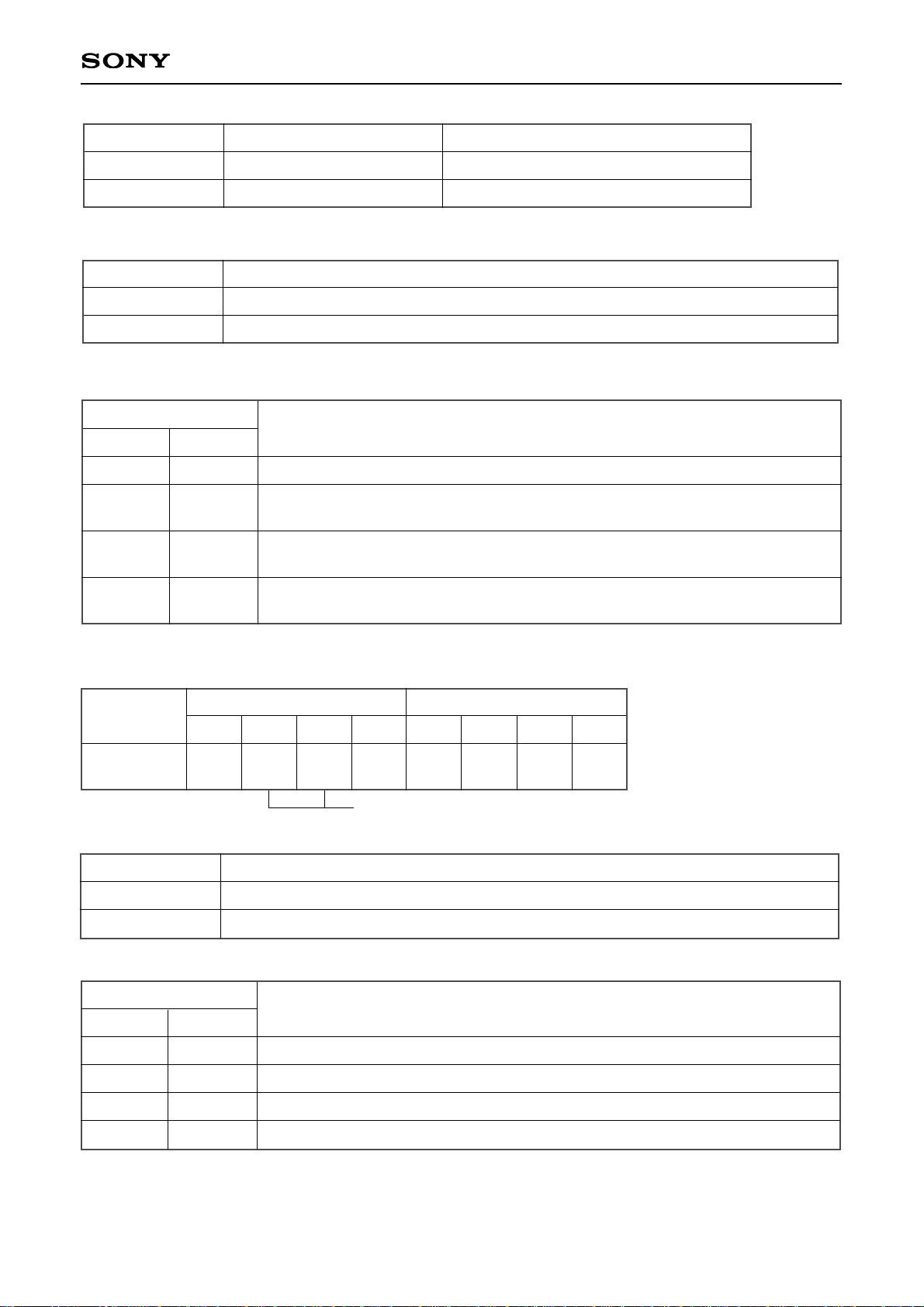
– 46 –
CXD3029R
Command bit
Processing
VCOSEL2 = 0
VCOSEL2 = 1
Multiplier PLL VCO2 is set to normal speed.
Multiplier PLL VCO2 is set to approximately twice the normal speed.
Command bit
KSL3 KSL2
Processing
Output of multiplier PLL VCO1 selected by VCO CS0 is 1/1 frequency-divided.
Output of multiplier PLL VCO1 selected by VCO CS0 is 1/2 frequency-divided.
Output of multiplier PLL VCO1 selected by VCO CS0 is 1/4 frequency-divided.
Output of multiplier PLL VCO1 selected by VCO CS0 is 1/8 frequency-divided.
0
0
1
1
0
1
0
1
See above.
Command
Data 2
MODE
specification
VCO
SEL2
ASHS SOCT0
VCO
SEL1
D3 D2 D1 D0
Data 3
KSL3 KSL2 KSL1 KSL0
D3 D2 D1 D0
Command bit
Sync protection window width
WSEL = 1
WSEL = 0
±26 channel clock
±6 channel clock
Anti-rolling is enhanced.
Sync window protection is enhanced.
Application
∗
In normal-speed playback, channel clock = 4.3218MHz.
Command bit
Function
ASHS = 0
ASHS = 1
The command transfer rate from the auto sequencer to the DSSP block is set to normal speed.
The command transfer rate from the auto sequencer to the DSSP block is set to half speed.
∗
See "§4-8. CD-DSP Block Playback Speed" for settings.
Command bit
SOCT0 SOCT1
Processing
Subcode-Q is output from the SQSO pin.
The spindle speed measurement result is output from the SQSO pin. Input the
readout clock to SQCK. (See Timing Chart 2-5.)
Various signals are output from the SQSO pin. Input the readout clock to SQCK.
(See Timing Chart 2-4.)
The error rate is output from the SQSO pin. Input the readout clock to SQCK.
(See Timing Chart 2-6.)
0
0
1
1
0
1
0
1
∗
$8X command TXOUT = 0 and $A8X command SDTO OUT = 0 must be set.
Page 47

– 47 –
CXD3029R
Command bit
Processing
VCOSEL1 = 0
VCOSEL1 = 1
Wide-band PLL VCO1 is set to normal speed.
Wide-band PLL VCO1 is set to approximately twice the normal speed.
Command bit
KSL1 KSL0
Processing
Output of wide-band PLL VCO2 is 1/1 frequency-divided.
Output of wide-band PLL VCO2 is 1/2 frequency-divided.
Output of wide-band PLL VCO2 is 1/4 frequency-divided.
Output of wide-band PLL VCO2 is 1/8 frequency-divided.
0
0
1
1
0
1
0
1
∗
Block Diagram of VCO Internal Path
Selector
1/2
1/1
1/8
1/4
Selector
To DSP interior
KSL3, 2
VCO1CS1, 0
No.2 VCO1
No.3 VCO1
No.4 VCO1
VCO1SEL
No.1 VCO1
1/2
1/1
1/8
1/4
Selector
To DSP interior
KSL1, 0
VCO2
VCO2SEL
VCO1 internal path
VCO2 internal path
Page 48

– 48 –
CXD3029R
D3
VCO1
CS1
VCO1
CS0
0 0 ERC4
SCOR
SEL
SCSY SOCT1 TXON TXOUT OUTL1 OUTL0
D2 D1 D0 D3 D2 D1 D0 D3 D2 D1 D0
Data 4 Data 5 Data 6
Command
MODE
specification
See page 45.
∗
The CXD3029R has four multiplier PLL VCO1s, and this command selects one of these VCO1s.
The four VCOs are No. 4, No. 3, No. 2 and No. 1 in order of the maximum frequency.
∗
The block diagrams for VCO1 and VCO2 including VCOSEL1, VCOSEL2, KSL0 to KSL3, VCO1CS0 and
VCO1CS1 are shown on the previous page.
Command bit
VCO1CS1 VCO1CS0
Processing
Selects the No. 1 VCO1.
Selects the No. 2 VCO1.
Selects the No. 3 VCO1.
Selects the No. 4 VCO1.
0
0
1
1
0
1
0
1
$8X commands cont.
Page 49

– 49 –
CXD3029R
Command bit
TXON = 0
Processing
When CD TEXT data is not demodulated, set TXON to "0".
When CD TEXT data is demodulated, set TXON to "1".
∗
See "§4-15. CD TEXT Data Demodulation".
TXON = 1
Command bit
Processing
SCSY = 0
SCSY = 1
No processing.
GRSCOR (protected SCOR) synchronization is applied again.
∗
Used to resynchronize GRSCOR.
The rising edge signal of this command bit is used internally, so when resynchronizing GRSCOR, first return
the setting to "0" and then set to "1".
GRSCOR is the crystal accuracy SCOR signal obtained by removing the motor wow component.
This signal is synchronized with PCMDATA.
The resynchronization conditions are when GTOP = high.
Command bit
TXOUT = 0
Processing
Various signals except for CD TEXT are output from the SQSO pin.
CD TEXT data is output from the SQSO pin.
∗
See "§4-15. CD TEXT Data Demodulation".
TXOUT = 1
Command bit
OUTL1 = 0
Processing
WDCK and XPCK are output.
WDCK and XPCK outputs are set low.OUTL1 = 1
Command bit
OUTL0 = 0
OUTL0 = 1
Processing
PCMD, BCK and LRCK are output.
PCMD, BCK and LRCK outputs are set low.
Command bit
Processing
SCOR SEL = 0
SCOR SEL = 1
WDCK signal is output.
GRSCOR (protected SCOR) is output.
∗
Used when outputting GRSCOR from the WDCK pin.
Command bit
Processing
ERC4 = 0
ERC4 = 1
C2 error double correction is performed when DSPB = 1.
C2 error quadruple correction is performed even when DSPB = 1.
Page 50

– 50 –
CXD3029R
Command
Data 1
Function
specification
1
DSPB
ON-OFF
A.SEQ
ON-OFF
1
D3 D2 D1 D0
Data 2
BiliGL
MAIN
BiliGL
SUB
FLFC
D3 D2
D1
0
D0
$9X commands
Command bit
DSPB = 0
DSPB = 1
Normal-speed playback, C2 error quadruple correction.
Double-speed playback, C2 error double correction. (quadruple correction when ERC4 = 1)
Processing
Normally FLFC = 0.
In CAV-W mode, set FLFC to "1" independently of the playback speed.
Command bit
BiliGL SUB = 0
BiliGL SUB = 1
STEREO
SUB
MAIN
Mute
BiliGL MAIN = 0
BiliGL MAIN = 1
Definition of bilingual capable MAIN, SUB and STEREO
The left channel input is output to the left and right channels for MAIN.
The right channel input is output to the left and right channels for SUB.
The left and right channel inputs are output to the left and right channels, respectively, for STEREO.
Command bit
Processing
OUTL2 = 0
OUTL2 = 1
WFCK is output.
WFCK is set low.
Command
MODE
specification
Data 7
0 0 OUTL2 0
D3 D2 D1 D0
Command
Data 3 Data 4
Data 5
D3 D2 D1 D0 D3 D2 D1 D0 D3 D2 D1 D0
000010010000
Function
specification
∗
The $A7X command XOE OUT must be set to "0".
Page 51

– 51 –
CXD3029R
Command
Data 6
Function
specification
0000
D3 D2 D1 D0
Data 7
DIV4 0 0 0
D3 D2 D1 D0
Command bit
DIV4 = 0
DIV4 = 1
Digital PLL master clock; conventional mode. (preset)
Digital PLL master clock; 2/3 mode.
Processing
This switches the digital PLL master clock.
Either the conventional mode or the 2/3 mode (2/3 of the conventional clock) can be selected.
Note) Do not set DIV4 to "1" when DSPB = 0.
Command
Data 1
Audio CTRL 0 0 Mute ATT
D3 D2 D1 D0
Data 2
PCT1 PCT2
D3 D2
0 SOC2
D1 D0
$AX commands
Command bit
Mute = 0
Mute = 1
Mute off if other mute
conditions are not set.
Mute on. Peak register reset.
Meaning
Command bit
ATT = 0
ATT = 1
Attenuation off.
–12dB
Meaning
Mute conditions
(1) When register A mute = 1.
(2) When register 8 DOUT Mute F = 1 and Digital Out is on ($B command MD2 = 1).
(3) When GFS stays low for over 35ms (during normal-speed).
(4) When register 9 BiliGL MAIN = Sub = 1.
(5) When register A PCT1 = 1 and PCT2 = 0.
(1) to (3) perform zero-cross muting with a 1ms time limit.
Command bit
PCT1
0
0
1
1
PCT2
0
1
0
1
Normal mode
Level meter mode
Peak meter mode
Normal mode
× 0dB
× 0dB
Mute
× 0dB
C1: double; C2: quadruple
C1: double; C2: quadruple
C1: double; C2: double
C1: double; C2: double
Meaning
PCM Gain
ECC error correction ability
Page 52

– 52 –
CXD3029R
Description of level meter mode (see Timing Chart 1-4.)
• When the LSI is set to this mode, it performs digital level meter functions.
• When the 96-bit clock is input to SQCK, 96 bits of data are output to SQSO.
The initial 80 bits are subcode-Q data (see "[2] Subcode Interface"). The last 16 bits are LSB first, which are
15-bit PCM data (absolute values) and an L/R flag.
The final bit (L/R flag) is high when the 15-bit PCM data is from the left channel and low when the data is
from the right channel.
• The PCM data is reset and the L/R flag is inverted after one readout.
Then the measurement for the maximum value continues until the next readout.
Description of peak meter mode (see Timing Chart 1-5.)
• When the LSI is set to this mode, the maximum PCM data value is detected regardless of if it comes from the
left or right channel.
The 96-bit clock must be input to SQCK to read out this data.
• When the 96-bit clock is input, 96 bits of data are output to SQSO and the value is set in the LSI internal
register again.
In other words, the PCM maximum value register is not reset by the readout.
• To reset the PCM maximum value register to "0", set PCT1 = PCT2 = 0 or set the $AX command Mute.
• The subcode-Q absolute time is automatically controlled in this mode.
In other words, after the maximum value is generated, the absolute time for CRC to become OK is retained in
the memory. Normal operation is conducted for the relative time.
• The final bit (L/R flag) of the 96-bit data is normally "0".
• The pre-value hold and average value interpolation data are fixed to level (–∞) for this mode.
SENS output switching
• This command is used to output the SQSO pin signal from the SENS pin.
When SOC2 = 0, SENS output is performed as usual.
When SOC2 = 1, the SQSO pin signal is output from the SENS pin.
At this time, the readout clock is input to the SCLK pin.
Note) Perform the SOC2 switching when SQCK = SCLK = high.
Command bit
SOC2 = 0
SOC2 = 1
The SENS signal is output from the SENS pin as usual.
The SQSO pin signal is output from the SENS pin.
Processing
Command
Data 3 Data 4
Data 5 Data 6
D3 D2 D1 D0 D3 D2 D1 D0 D3 D2 D1 D0 D3 D2 D1 D0
0000010000000000
Audio CTRL
Page 53

– 53 –
CXD3029R
$A4 commands (preset: $A4C800)
Data 1
D30D21D10D00D3
RSL1D2RSL0
D10D00D3
DTSL1D2DTSL0D1MCSL1D0MCSL0
D30D2
SDSL
2
D1
SDSL
1
D0
SDSL
0
A4
(Signal select)
Data 2 Data 3 Data 4
Command
D3
EN
XSOE
D2
CKOUT
SL2
D1
CKOUT
SL1
D0
SLD
BBIN
D3
max
C2PO7
D2
max
C2PO6
D1
max
C2PO5
D0
max
C2PO4
D3
max
C2PO3
D2
max
C2PO2
D1
max
C2PO1
D0
max
C2PO0
Data 5 Data 6 Data 7
RSL1 RSL0
Processing
The external buffer RAM is set to 4M bits.
No selected.
The external buffer RAM is set to 16M bits.
0
1
1
∗
0
0
1
RSL1, RSL0: These bits set the external buffer RAM.
∗: preset
DTSL1, DTSL0
: See the second half of the description of $A4 commands.
MCSL1: This bit sets the DAC block master clock.
When "0", the DAC block master clock is set to 16.9344MHz (384fs). (default)
When "1", the DAC block master clock is set to 33.8688MHz (768fs).
MCSL0: This bit sets the shock-proof memory controller block master clock.
When "0", the shock-proof memory controller block master clock is set to 16.9344MHz (384fs).
(default)
When "1", the shock-proof memory controller block master clock is set to 33.8688MHz (768fs).
ENXSOE: This bit switches the command input method.
When "0", the command transfer clock and the SENS serial data readout clock are input from
the respective pins. (default)
When "1", the command transfer clock and the SENS serial data readout clock are input from
the CLOK pin.
The clock input is switched with the XSOE pin. At this time, connect the SCLK pin to high.
ENXSOE XSOE pin
CLOK pin
SCLK pin
Command transfer clock input
Command transfer clock input
SENS serial data readout clock input
Command transfer clock input
SENS serial data readout clock input
SENS serial data readout clock input
Connect to high.
Connect to high.
0
0
1
1
L
H
L
H
In addition, when ENXSOE is set to "1" and the SQSO pin signal output is read from the SENS
pin, the command input method is as follows.
At this time, connect the SCLK and SQCK pins to high.
See the command descriptions for $A command SOC2 and $8 commands TXOUT, SOCT0
and SOCT1.
Page 54
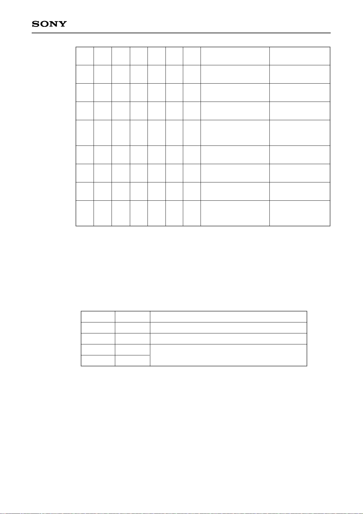
– 54 –
CXD3029R
ENXS
OE
XSOE
pin
$A
SOC2
$8
TXOUT
$8
SOCT0$8SOCT1
CLOK pin
SENS pin
Command transfer
clock input
SENS serial data
readout clock input
Subcode-Q readout
clock input
Readout clock input of
the spindle speed
measurement result
Various signal readout
clock input
Error rate readout clock
input
CD TEXT data readout
clock input
Readout clock input of
shock-proof memory
controller serial data
High or low output
SENS output
∗1
Subcode-Q output
Spindle speed
measurement result
output
∗2
Various signal
output
∗3
Error rate output
∗4
CD TEXT data
output
Shock-proof memory
controller serial data
output
1
1
1
1
1
1
1
1
$A8
SDTO
OUT
∗
∗
0
0
0
0
0
1
H
L
L
L
L
L
L
L
∗
0
1
1
1
1
1
1
∗
∗
0
0
0
0
1
∗
∗
∗
0
0
1
1
∗
∗
∗
∗
∗
1
0
1
∗
∗
∗: don't care
∗
1
See "§1-4. Description of SENS Signals" for the SENS output.
∗2
See Timing Chart 2-5 for the spindle speed measurement result.
∗3
The output signals are PER7 to PER0, FOK, GFS, LOCK, EMPH, ALOCK and VF9 to VF0.
For details, see Timing Chart 2-4.
∗4
For the error rate timing, see Timing Chart 2-6.
CKOUTSL2, CKOUTSL1:
These bits select the clock output from the R4M pin.
When the crystal is 16.9344MHz and XTSL = high, the output frequency is halved.
CKOUTSL2 CKOUTSL1
Processing
4.2336MHz output
8.4672MHz (R8M) output
4.2336MHz (C4M) output
Changes in CAV-W mode and variable pitch mode.
0
0
1
1
∗
0
1
0
1
∗: preset
DTSL1, DTSL0: These bits select the data output from the DOUT pin.
In external mode, the data input through the LRCKI, BCKI and PCMDI pins is used.
DOUT output in the following tables is valid when $34A commands DOUT EN1 and DOUT EN2
are both 1. In this case, see "$34A commands".
When $34A commands DOUT EN1 and DOUT EN2 are both 0, see "§4-5-2. Digital Out from
DA Interface Input".
At this time, the data from the CD DSP is output from the DOUT pin with a subcode is added.
SDSL2, SDSL1: These bits select the data input to the DAC block and the data output from the PCMD pin.
SLDBBIN: This bit selects the data input to the DAC block and the data output from the PCMD and
DOUT pins.
Page 55

– 55 –
CXD3029R
When SLDBBIN = 0, the internally connected data is selected. (default)
DTSL1
0
0
0
0
0
0
0
0
1
1
1
1
1
1
1
1
0
0
0
0
1
1
1
1
0
0
0
0
1
1
1
1
0
0
1
1
0
0
1
1
0
0
1
1
0
0
1
1
0
1
0
1
0
1
0
1
0
1
0
1
0
1
0
1
0
∗
1
0
∗1
0
∗1
0
∗1
0
∗1
0
∗1
0
∗1
0
∗1
DSP mode
Shock-proof
memory controller
mode
DSP mode
Shock-proof
memory controller
mode
DSP mode
Shock-proof
memory controller
mode
DSP mode
Shock-proof
memory controller
mode
DSP & DAC mode
Shock-proof
memory controller
& DAC mode
DSP mode
Shock-proof
memory controller
mode
DSP mode
External mode
DSP mode
DSP & DAC mode
Shock-proof memory
controller mode
Shock-proof memory
controller & DAC mode
DSP mode
DSP & DAC mode
Shock-proof memory
controller mode
Shock-proof memory
controller & DAC mode
DSP mode
DSP & DAC mode
Shock-proof memory
controller mode
Shock-proof memory
controller & DAC mode
DSP mode
DSP & DAC mode
Shock-proof memory
controller mode
Shock-proof memory
controller & DAC mode
DTSL0 SDSL2 SDSL1 SDSL0 Input to DAC block DOUT output PCMD output
∗
∗: preset
∗
1
: The relationship between LRCK, BCK and PCMD changes according to the setting value.
When SDSL0 = 0, the LRCK, BCK and PCMD phase difference is constant but the LRCK frequency
changes when SDSL0 is switched.
When SDSL0 = 1, the LRCK frequency is constant but the phase difference between LRCK, BCK and
PCMD changes before and after SDSL1 is switched. When not switching the output data selection, set
SDSL1 and SDSL0 to the same value.
max C2PO7 to max C2PO0:
These bits set the C2PO conditions.
max C2PO7 to max C2PO0
Processing
The C2PO upper limit value reflected to mon C2PO and
added to the write prohibited condition.
00000000 to 11111111
Page 56

– 56 –
CXD3029R
DTSL1
0
0
0
0
0
0
0
0
1
1
1
1
1
1
1
1
0
0
0
0
1
1
1
1
0
0
0
0
1
1
1
1
0
0
1
1
0
0
1
1
0
0
1
1
0
0
1
1
0
1
0
1
0
1
0
1
0
1
0
1
0
1
0
1
0
∗
1
0
∗1
0
∗1
0
∗1
0
∗1
0
∗1
0
∗1
0
∗1
External mode
External & DAC mode
DSP mode
Shock-proof memory
controller mode
DSP mode
External mode
DSP mode
External & DAC mode
Shock-proof memory
controller mode
External & DAC mode
DSP mode
External & DAC mode
Shock-proof memory
controller mode
External & DAC mode
DSP mode
External & DAC mode
Shock-proof memory
controller mode
External & DAC mode
DSP mode
External & DAC mode
Shock-proof memory
controller mode
External & DAC mode
DTSL0 SDSL2 SDSL1 SDSL0 Input to DAC block DOUT output PCMD output
When SLDBBIN = 1, the data input from the LRCKI, BCKI and PCMDI pins is selected.
∗
1
: The relationship between LRCK, BCK and PCMD changes according to the setting value.
When SDSL0 = 0, the LRCK, BCK and PCMD phase difference is constant but the LRCK frequency
changes when SDSL0 is switched.
When SDSL0 = 1, the LRCK frequency is constant but the phase difference between LRCK, BCK and
PCMD changes before and after SDSL1 is switched. When not switching the output data selection, set
SDSL1 and SDSL0 to the same value.
Page 57
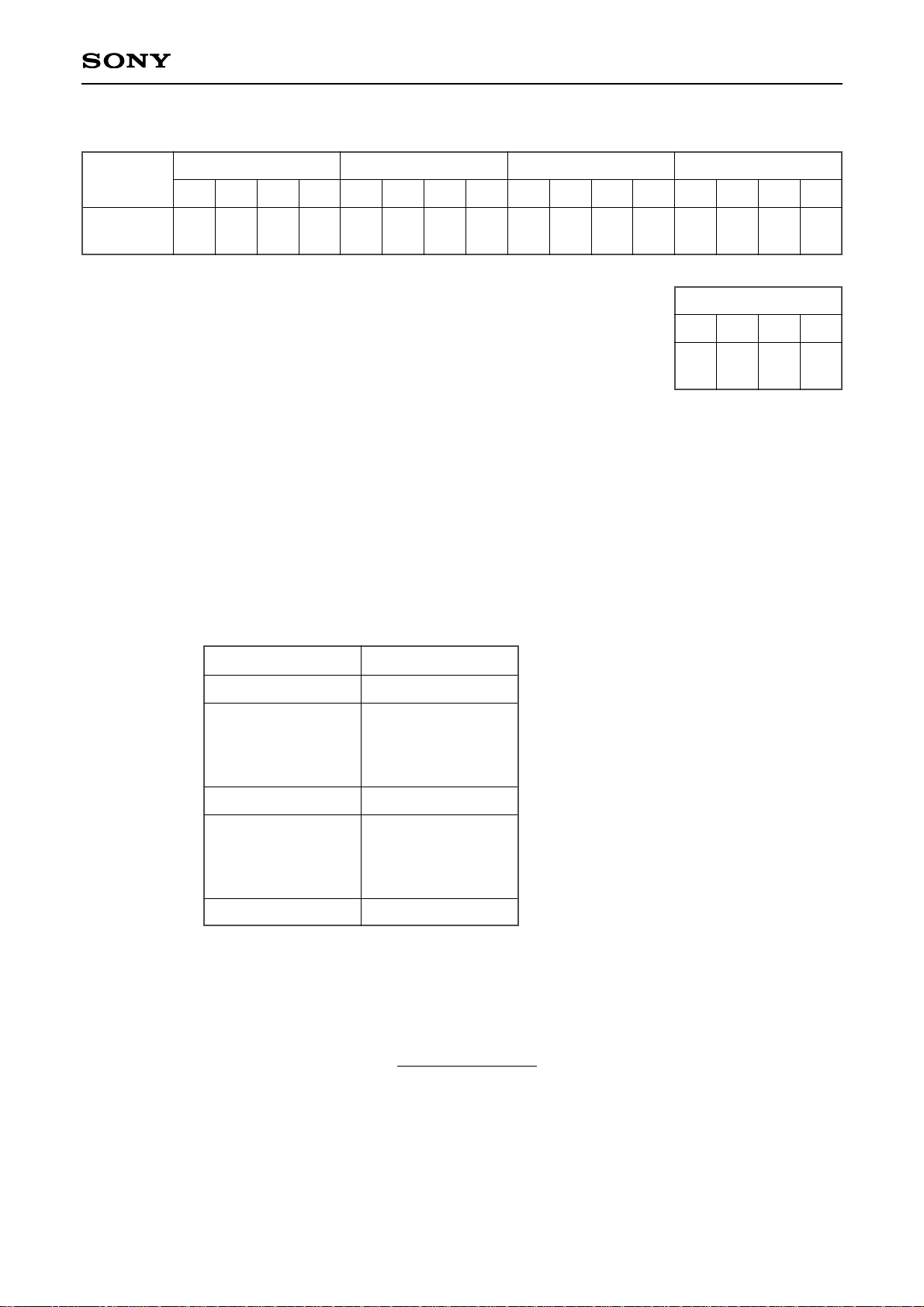
– 57 –
CXD3029R
$A5 commands (when Data 2 D3 = 0, D2 = 0) (preset: $A50400)
Data 1
D3
0
D2
1
D10D01D30D20D11D0
ZMUTAD3SMUT
D2
AD10D1AD9D0AD8D3AD7D2AD6
D1 D0
AD5 AD4
A5
(Bass boost)
Data 2 Data 3 Data 4
Command
D3
AD3D2AD2D1AD1D0AD0
Data 5
ZMUTA: This bit sets the zero detection analog mute on/off.
When "0", zero detection analog mute is on. (default)
When "1", zero detection analog mute is off.
When zero data is detected for both the left and right channels, the LPF block output is set to
center output.
SMUT: This bit sets the soft mute on/off.
When "0", soft mute is off. (default)
When "1", soft mute is on.
AD10 to AD0: These bits set the attenuation data. The attenuation data consists of 11 bits, and is set as
follows.
Attenuation data Audio output
7FF (h)
7FE (h)
:
402 (h)
401 (h)
400 (h)
3FF (h)
3FE (h)
:
001 (h)
000 (h)
+6.02dB
+6.016dB
:
+0.017dB
+0.0085dB
0dB
–0.0085dB
–0.017dB
:
–60.206dB
–∞
∗
The audio output from 001 (h) to 7FF (h) is obtained using the
following equation:
Audio data output = 20 log [dB]
Attenuation data
1024
∗: preset
Page 58

– 58 –
CXD3029R
$A5 commands (when Data 2 D3 = 0, D2 = 1) (preset: $A540A4)
Data 1
D30D21D10D01D30D21D1
PWDND0ZDPLD3WOC
D2
DAC
EMPH
D1
HiCut
FILTER
D0
BST
CL
D31D20D1
OBIT1D0OBIT0
A5
(Bass boost)
Data 2 Data 3 Data 4
Command
D30D21D10D0
0
Data 5
PWDN: This bit sets the DAC block operation mode.
When "0", the DAC block clock is stopped. This makes it possible to reduce power
consumption. (default)
When "1", the DAC block operates normally.
ZDPL: This bit sets the zero detection flag polarity.
When "0", the LRMU pin is set low during mute. (default)
When "1", the LRMU pin is set high during mute.
WOC: When WOC = 1, the DAC sync window opens. This is used to synchronize the DAC.
DAC EMPH: This bit sets the digital de-emphasis on/off.
When "0", digital de-emphasis is off. (default)
When "1", digital de-emphasis is on.
HiCutFILTER: This bit sets the high-cut filter on/off.
When "0", the high-cut filter is off. (default)
When "1", the high-cut filter is on.
BSTCL: This bit sets the bass boost level clear on/off.
1: On; the set bass boost level is cleared to 0dB.
0: Off; normal operation (default)
OBIT1, OBIT0: These bits set the word length of the serial data output from the PCMD pin.
The serial data word length can be selected only when the data output from the PCMD pin is
set to DAC output.
OBIT1 OBIT0
Serial data word length
20 bits
18 bits
16 bits
0
0
1
∗
0
1
0
∗: preset
Page 59
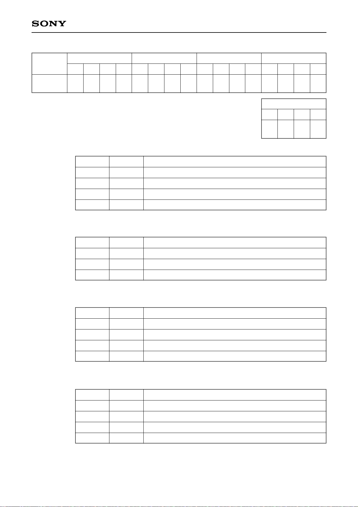
– 59 –
CXD3029R
$A5 commands (when Data 2 D3 = 1, D2 = 0) (preset: $A58000)
Data 1
D30D21D10D01D31D20D1
BBON1D0BBON0D3HBON1D2HBON0D1BBSL1D0BBSL0D3HBSL1D2HBSL0
D1
BBST
Vdwn1
D0
BBST
Vdwn0
A5
(Bass boost)
Data 2 Data 3 Data 4
Command
D3
BBST
Vup1
D2
BBST
Vup0
D1
BBST
Uth
D0
BBST
Lth
Data 5
BBON1, BBON0: These bits set the bass boost on/off and the turnover frequency.
BBON1 BBON0
Processing
Bass boost is off.
Bass boost is on and the turnover frequency is set to 125Hz.
Bass boost is on and the turnover frequency is set to 160Hz.
Bass boost is on and the turnover frequency is set to 200Hz.
0
0
1
1
∗
0
1
0
1
∗: preset
HBON1, HBON0: These bits set the high boost on/off and the turnover frequency.
HBON1 HBON0
Processing
High boost is off.
High boost is on and the turnover frequency is set to 5kHz.
High boost is on and the turnover frequency is set to 7kHz.
0
1
1
∗
0
0
1
∗: preset
BBSL1, BBSL0: These bits set the boost level for bass boost.
BBSL1 BBSL0
Processing
The boost level for bass boost is set to 10dB.
The boost level for bass boost is set to 14dB.
The boost level for bass boost is set to 18dB.
The boost level for bass boost is set to 22dB.
0
0
1
1
∗
0
1
0
1
∗: preset
HBSL1, HBSL0: These bits set the boost level for high boost.
HBSL1 HBSL0
Processing
The boost level for high boost is set to 4dB.
The boost level for high boost is set to 6dB.
The boost level for high boost is set to 8dB.
The boost level for high boost is set to 10dB.
0
0
1
1
∗
0
1
0
1
∗: preset
Page 60

– 60 –
CXD3029R
BBST Vdwn1, BBST Vdwn0: These bits set the boost attack time (Vol Down) for bass and high boost.
BBST Vdwn1
BBST Vdwn0
Processing
The boost attack time for bass and high boost is set to standard.
The boost attack time for bass and high boost is set to fast.
The boost attack time for bass and high boost is set to slow.
0
0
1
∗
0
1
1
∗: preset
BBST Vup1, BBST Vup0: These bits set the boost release time (Vol Up) for bass and high boost.
BBST Vup1 BBST Vup0
Processing
The boost release time for bass and high boost is set to standard.
The boost release time for bass and high boost is set to fast.
The boost release time for bass and high boost is set to slow.
0
0
1
∗
0
1
1
∗: preset
BBST Uth: This bit sets the bass and high boost Uth.
When "0", Uth is set to –1.9dB. (default)
When "1", Uth is set to –0.9dB.
BBST Lth: This bit sets the bass and high boost Lth.
When "0", Lth is set to –12dB. (default)
When "1", Lth is set to –4.4dB.
∗
When the volume rises above Uth, the boost level is reduced. The speed at which the boost level is reduced
is the attack time.
When the volume falls below Lth, the boost level is increased up to the setting value. The speed at which the
boost level is increased is the release time.
$A5 commands (when Data 2 D3 = 1, D2 = 1) (preset: $A5C000)
Data 1
D30D21D10D01D31D21D1
COMP
ON
D00D30D20D10D00D30D20D11D0
0
A5
(Bass boost)
Data 2 Data 3 Data 4
Command
D30D20D10D0
PDM
INV
Data 5
COMP ON: This bit sets the compressor on/off.
When "0", the compressor is off. (default)
When "1", the compressor is on.
PDM INV: This bit sets the DAC block PDM signal polarity.
When "0", the polarity is set to non-inverted. (default)
When "1", the polarity is set to inverted.
$A6 commands: Commands for the headpphone volume circuit.
The command processing is the same as for $A5.
Page 61
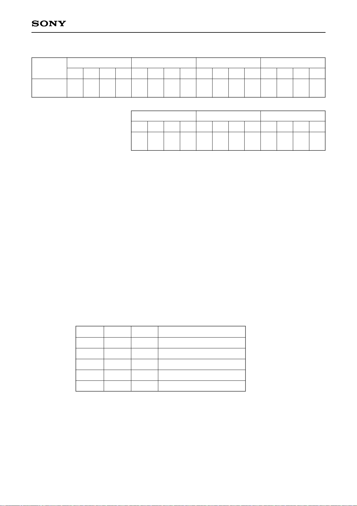
– 61 –
CXD3029R
SL XQOK: This bit sets the XQOK control mode.
When "0", XQOK should be controlled for the period from when SCOR goes high until
GRSCOR goes high. (default)
When "1", XQOK should be controlled for the period while GRSCOR is high.
SL XWRE: This bit sets the XWRE control mode.
When "0", XWRE should be controlled for the period from when SCOR goes high until
GRSCOR goes high. (default)
When "1", XWRE should be controlled for the period while GRSCOR is high.
GTOP CHECK:This bit controls GRSCOR generation when GTOP is high.
When "0", the GRSCOR generation circuit is not resynchronized even when GTOP is high.
When "1", the GRSCOR generation circuit is resynchronized when GTOP goes high. (default)
NOLIM WDCK: Always set to "1".
SPSL COM: This bit sets whether to control XQOK, XWRE and XRDE with pins or serial data.
When "0", XQOK, XWRE and XRDE should be controlled with pins. (default)
When "1", XQOK, XWRE and XRDE should be controlled with serial data ($A8).
Note) The Data 3 D3 and Data 6 D1 bits should be switched somultaneously.
READ2,
READS2, READS1
:This bit sets the audio data readout speed from the shock-proof memory controller block.
$A7 commands (preset: $A7200000)
Data 1
D30D21D11D01D3
SL
XQOK
D2
SL
XWRE
D1
GTOP
CHECK
D0
NOLIM
WDCK
D3
SPSL
COM
D2
READ2
D1
REF
SEL
D0
REF
ON
D3
XOE
OUT
D2
MSL2D1MSL1D0MSL0
A7
(Shock-proof
memory setting)
Data 2 Data 3 Data 4
Command
D3
ADDRST
SEL
D2
ADRMO
D1
GRSCOR
MOD
D0
STA
SEL
D3
XWI
H2
D2
XWI
H1
D1
SPSL
COM
D0
WQR
MON
D3
A11
SEL
D2
READ
S2
D1
READ
S1
D0
MON
SEL
Data 5 Data 6 Data 7
READ2
0
0
0
0
1
0
0
1
1
∗
0
1
0
1
∗
1× speed readout
0.5× speed readout
0.25× speed readout
—
2× speed readout
READS2 READS1 Readout speed setting
∗
∗: preset
The shock-proof memory controller interior should be resynchronized after the readout speed
is switched. Execute the $AAX ADPWO command for resynchronization.
Page 62

– 62 –
CXD3029R
MSL2
0
0
0
0
1
1
1
1
0
0
1
1
0
0
1
1
0
1
0
1
0
1
0
1
The entire DRAM area can be used as audio data.
32K bits
64K bits
128K bits
256K bits
512K bits
1M bits
2M bits
MSL1 MSL0 DRAM area that can be accessed from the microcomputer
∗
∗: preset
REF SEL: This bit sets the DRAM refresh rate. (Use this bit in conjunction with the $AC command
REFSEL2.)
REF ON: This bit sets the DRAM refresh function on/off.
When "0", the refresh function is off. (default)
When "1", the refresh function is on.
XOE OUT: This bit switches the WFCK pin output mode.
When “0”, WFCK is output from the WFCK pin. (default)
When “1”, XOE is output from the WFCK pin.
MSL2 to MSL0: These bits set the DRAM area that can be accessed from the microcomputer.
REFSEL2
0
0
1
1
0
1
0
1
11.51ms/2048 times
5.81ms/2048 times
46.44ms/2048 times
23.22ms/2048 times
REFSEL1 Refresh rate
∗
∗: preset
ADDRST SEL: This bit selects the address reset mode.
When "0", the conventional address reset is used. (default)
When "1", the address is reset by the ADDRST command.
ADRMO: This bit selects the remaining valid addresses.
When "0", the conventional remaining valid addresses are displayed. (default)
When "1", the remaining addresses from 0000000 to 1111111 are displayed.
GRSCOR MOD
: This bit selects the GRSCOR mode.
When "0", the conventional 64-frame GRSCOR is output. (default)
XWIH2: The XWIH condition addition is selected.
When “0”, the condition is added. (default)
When “1”, the write speed condition is added to the write prohibited condition.
XWIH1: The XWIH condition addition is selected.
When “0”, the condition is not added. (default)
When “1”, the condition of failure access to DRAM is added to the write prohibited condition.
Page 63

– 63 –
CXD3029R
WQR MON: This bit selects the XWRE, XQOK and XRDE outputs.
When "0", XWRE, XQOK and XRDE output is prohibited. (default)
When "1", XWRE, XQOK and XRDE output is allowed.
A11 SEL: This bit selects the A11 pin function.
When "0", the A11 pin is used as the A11 pin. (default)
When "1", the A11 pin is used as a low-active write prohibit factor.
STA SEL: This bit selects the shock-proof memory controller status output.
When "1", the conventional ESP status is output. (See §4-13-3.)
When "0", the new shock-proof memory controller status is output. (default)
The status readout when STA SEL = 0 is as follows.
MONSEL: This bit selects the COUT, XUGF, MIRR and XPCK pin functions.
When "0", these pins output the signals corresponding to the SRO1, MTSL1 and MTSL0
commands. (See the table on page 8.)
When "1", these pins output SCOR, QRCVD, SCOR WINDOW and GTOP, respectively.
D0
D1
D2
D3
D4
D5
D6
D7
D8
D9
D10
D11
D12
D13
D14
D15
D16
D17
D18
D19
D20
D21
D22
D23
Signal
XWPHD
QRCVD
XEMP
monGRSCOR
monC2PO
GTOP
monSCOR
AM13
AM14
AM15
AM16
AM17
AM18
AM19
AM20
AM21
—
—
monADPCM
XFUL
ROF
SPOVER
NOWR
—
Description
0: Write prohibited
1: Address updated
0: No valid data
1: GRSCOR present
1: C2PO of the setting value or higher present
1: GTOP present in the preceding GRSCOR
1: SCOR generated normally (no interpolation)
Address monitor
Address monitor
Address monitor
Address monitor
Address monitor
Address monitor
Address monitor
Address monitor
Address monitor
Don't care.
Don't care.
1: ADPCM compression error
0: No write area
1: The DSP SRAM has overflowed.
1: The speed limit is exceeded for more than the set number
during one GRSCOR.
1: Access is failed in the shock-proof memory controller.
Don’t care.
Page 64

– 64 –
CXD3029R
$A8 commands (preset: $A8F8)
Data 1
D31D20D10D00D3
XQOKD2XWRED1XRDED0XSOEO
D3
XSOEO
2
D2
ADDRST
D1
SCOR
MOD
D0
SDTO
OUT
D3 D2 D1 D0
A8
(Shock-proof
memory control)
Data 2 Data 3 Data 4
Command
XQOK, XWRE, XRDE:
When $A7 command SPSL COM = 1, XQOK, XWRE and XRDE are controlled with serial data.
(default: 1)
XSOEO: This bit controls the serial data from the shock-proof block.
Shock-proof block data is loaded to the serial readout register by detecting the falling edge of
XSOEO.
XSOEO2: This bit is used when the microcomputer reads data from the DRAM. (default: 1)
The shock-proof memory controller block loads the data from the DRAM to the serial readout
register by detecting the fall of XSOEO2.
ADDRST: This command is valid when $A7 command ADDRST SEL = 1.
When "0", no operations are performed. (default)
When "1", the VWA, WA and RA are all reset.
SCOR MOD: This bit selects the SCOR interpolation mode.
When "0", SCOR, which is read from the disc, is output. (default)
When "1", SCOR, which interpolated in the IC, is output.
SDTO OUT: This bit is used to output serial data from the shock-proof block to the SQSO pin.
When "0", various signals are output from the SQSO pin. For details on these signals, see
$8X commands SOCT1, SOCT0 and TXOUT. (default)
When "1", the shock-proof block serial data is output from the SQSO pin.
Page 65

– 65 –
CXD3029R
$A9 commands (preset: $A90000)
Data 1
D31D20D10D01D3
SubQA
3
D2
SubQA
2
D1
SubQA
1
D0
SubQA
0
D30D20D10D00D3
SubQD
7
D2
SubQD
6
D1
SubQD
5
D0
SubQD
4
A9
(DOUT subcode-Q
setting)
Data 2 Data 3 Data 4
Command
D3
SubQD
3
D2
SubQD
2
D1
SubQD
1
D0
SubQD
0
D3 D2 D1 D0 D3 D2 D1 D0
Data 5 Data 6 Data 7
SubQA3 to SubQA0, SubQD7 to SubQD0:
These bits set the Ubit inside the DOUT generation circuit in the DAC block. Note that these
bits have no effect on the DOUT generation circuit in the CD DSP block.
Control, address
Movement number
INDEX number
Elapsed time within a
movement (minutes)
Elapsed time within a
movement (seconds)
Elapsed time within a
movement (frames)
(Set to "0".)
Absolute time (minutes)
Absolute time (seconds)
Absolute time (frames)
(Control command)
0
0
0
0
0
0
0
0
1
1
1
SubQA3 SubQA2 SubQA1 SubQA0 SubQD7 SubQD6 SubQD5 SubQD4 SubQD3 SubQD2 SubQD1 SubQD0
Setting contents
0
0
0
0
1
1
1
1
0
0
0
0
0
1
1
0
0
1
1
0
0
1
0
1
0
1
0
1
0
1
0
1
0
Q1
Q9
Q17
Q25
Q33
Q41
Q49
Q57
Q65
Q73
DON
Q2
Q10
Q18
Q26
Q34
Q42
Q50
Q58
Q66
Q74
DCL
Q3
Q11
Q19
Q27
Q35
Q43
Q51
Q59
Q67
Q75
DUP1
Q4
Q12
Q20
Q28
Q36
Q44
Q52
Q60
Q68
Q76
DUP0
Q5
Q13
Q21
Q29
Q37
Q45
Q53
Q61
Q69
Q77
DLD
Q6
Q14
Q22
Q30
Q38
Q46
Q54
Q62
Q70
Q78
0
Q7
Q15
Q23
Q31
Q39
Q47
Q55
Q63
Q71
Q79
0
Q8
Q16
Q24
Q32
Q40
Q48
Q56
Q64
Q72
Q80
0
DON: This bit sets the Ubit output on/off inside the DOUT generation circuit in the DAC block.
When "0", Ubit is not output. (default)
When "1", Ubit is output.
DCL: This bit clears the elapsed time within a movement to "0".
The elapsed time is cleared to "0" at the falling edge of DCL (DCL = 1 → 0). (default: DCL = 1)
DUP1: This bit sets the absolute time counter operate/stop.
When "0", the absolute time counter is stopped. (default)
When "1", the absolute time counter operates.
DUP0: This bit sets the elapsed time within a movement counter operate/stop.
When "0", the elapsed time within a movement counter is stopped. (default)
When "1", the elapsed time within a movement counter operates.
DLD: This bit is used when setting the INDEX number, elapsed time within a movement, and absolute time.
When "0", the settings cannot be changed. (default)
When "1", the settings can be changed. Note that "0" is output for the INDEX number, elapsed
time within a movement, and absolute time while DLD = 1.
The control, address and movement number settings can be changed regardless of the DLD setting.
Page 66

– 66 –
CXD3029R
$A9E commands (preset: $A9E00000)
Data 1
D31D20D10D01D31D21D11D00D31D2
DRWRD1DRADR
D00D3
DRD15D2DRD14D1DRD13D0DRD12
A9E
(DRAM I/F)
Data 2 Data 3 Data 4
Command
D3
DRD11D2DRD10D1DRD9D0DRD8D3DRD7D2DRD6D1DRD5D0DRD4D3DRD3D2DRD2D1DRD1D0DRD0
Data 5 Data 6 Data 7
DRWR: This bit sets write/read for access from the microcomputer to the DRAM.
When "0", the read from DRAM mode is set. (default)
When "1", the write to DRAM mode is set.
DRADR: This bit sets the address control method for access from the microcomputer to the DRAM.
When "0", relative address control is set. (default)
When "1", absolute address control is set.
DRD15 to DRD0: These bits set the data to be written to the DRAM for access from the microcomputer to the
DRAM.
$A9F commands (preset: $A9F00000)
Data 1
D31D20D10D01D31D21D11D01D3
DADR19D2DADR18D1DADR17D0DADR16D3DADR15D2DADR14D1DADR13D0DADR12
A9F
(DRAM I/F)
Data 2 Data 3 Data 4
Command
D3
DADR11D2DADR10D1DADR9D0DADR8D3DADR7D2DADR6D1DADR5D0DADR4D3DADR3D2DADR2D1DADR1D0DADR0
Data 5 Data 6 Data 7
DADR19 to DADR0:
These bits set the DRAM address for access from the microcomputer to the DRAM.
Page 67

– 67 –
CXD3029R
$AA commands (preset: $AA00404)
Data 1
D31D20D11D00D3
ADPOND2BITSL1D1BITSL0
D00D3
ADPWO
D20D10D00D30D2
GRSEL
D10D0
0
AA
(Compression
setting)
Data 2 Data 3 Data 4
Command
ADPON: This bit sets audio data compressed/uncompressed.
When "0", the audio data uses uncompressed mode. (default)
When "1", the audio mode is compressed mode.
BITSL1, BITSL0: These bits set the audio data compression mode.
BITSL1 BITSL0
Compression mode
4 bits
6 bits
8 bits
0
0
1
∗
0
1
0
∗: preset
ADPWO: The CD-DSP block LRCK and shock-proof memory controller block LRCK are
resynchronized.
When “0”, not resynchronized. (default)
When “1”, resynchronized.
Note)•• Set the $AD command CDDSP SLEEP to 0 for resynchronization.
•
• ADPWO should be returned to “0” after ADPWO is set to “1” and one or more LRCK
cycle of CD-DSP block is waited.
GRSEL: This bit selects the GRSCOR signal output. Note that GRSCOR is output from the WDCK
pin when $8 command SCOR SEL = 1.
When "0", the GRSCOR signal generated by the CD DSP block is output.
When "1", the GRSCOR signal is output at the timing used inside the shock-proof memory
controller block. (default)
ADPCM SEL: This bit selects ADPCM compensation.
When "0", ADPCM is not compensated.
When "1", ADPCM is compensated.
ADPCM MUTE: This bit sets mute at ADPCM compensation.
When "0", it does not mute at ADPCM compensation.
When "1", it mutes at ADPCM compensation.
MLAT: This bit validate XLAT which is low for 6µs or more.
When “0”, the minimum value of XLAT low interval is 750ns.
When “1”, the minimum value of XLAT low interval is set to 6µs.
Note) 11µs or more should be necessary from the XLAT fall to the next command data
transfer when this function is used.
ORMU: This bit controls the output signal from the LRMU pin.
When “0”, the “0” detection flag for Lch and Rch (AND output) is output.
When “1”, the OR output is made with the “0” detection flag for Lch and Rch (AND output)
and SYSM.
D3
ADPCM
SEL
D2
ADPCM
MUTE
D10D00D3
MLATD2ORMU
D10D0
0
Data 5 Data 6
Page 68

– 68 –
CXD3029R
$AB commands (preset: $AB000000)
Data 1
D31D20D11D01D3
ARDTEN
D21D11D01D31D20D11D00D30D20D11D0
0
AB
(EFM playability
enhancement
setting)
Data 2 Data 3 Data 4
Command
D31D20D10D00D30D20D10D00D31D20D10D0
0
Data 5 Data 6 Data 7
ARDTEN: This is the EFM playability enhancement setting.
When "0", the EFM playability enhancement function is off.
When "1", the EFM playability enhancement function is on.
∗
Set this command in the condition when a disc is not being played back.
Page 69

– 69 –
CXD3029R
$AC commands (preset: $AC0C001)
Data 1
D31D21D10D00D3
AVWD20D1SFP5D0SFP4D3SFP3D2SFP2D1SFP1D0SFP0D30
D20D10D0
0
AC
(Sync expansion
specification)
Data 2 Data 3 Data 4
Command
AVW: This bit sets the sync protection window width automatic expansion function.
When "0", the sync protection window width automatic expansion function is off.
When "1", the sync protection window width automatic expansion function is on.
This setting is not affected by the sync forward protection times setting SFP5 to SFP0.
∗
The sync protection window width (±6 channel clocks when WSEL = 0, ±26 channel clocks
when WSEL = 1) is widened 32 channel clocks at a time each time a sync mark is inserted
during the interval from the 16th forward protection until GFS goes high. When the maximum
window width is reached (when the window width exceeds 588 channel clocks), GTOP goes
high.
SFP5 to SFP0: These bits set the frame sync forward protection times. The setting range is from 1 to 3F (h).
For details on frame sync protection, see "§4-2. Frame Sync Protection".
∗
Part of this command bit register is also used by $C SFP3 to SFP0. Of $AC SFP3 to SFP0 or
$C SFP3 to SFP0, the command bit setting made last is valid. When using an existing status,
set the value with $C SFP5 to SFP0. When using the $AC commands, set $AC SFP3 to
SFP0 to the value set by $C SFP3 to SFP0.
REFSEL2: This bit sets the refresh rate to DRAM.
See the description of $A7 command REFSEL.
SLIM1, 0: This bit sets the DRAM write speed limit value.
D3
REF
SEL2
D2
SLIM1D1SLIM0
D0
OV4D3OV3D2OV2D1OV1D0OV0
Data 5 Data 6
SLIM1
0
0
1
1
0
1
0
1
Up to 4.0× speed write
Up to 4.5× speed write
Up to 5.0× speed write
Up to 5.5× speed write
SLIM0 Write speed limit value
∗
∗: preset
OV4 to OV0
00000 to 11111 Can be set from 1 to 31 times.
Limit value of speed violation number
Preset value: 00001
Note) This command is valid when $A7X XWIH2 = 1.
OV4 to OV0: This bit sets the limit value of the speed violation number for one GRSCOR which is reflected
to XWIH.
Note) • The violation speed is set with the $AC commands SLIM 1 and 0.
• This command is valid when $A7X XWIH2 = 1.
Page 70

– 70 –
CXD3029R
$AD commands (preset: $AD040)
Data 1
D31D21D10D01D3
ADCPS
D2
DSP
SLEEP
D1
DSSP
SLEEP
D0
ASYM
SLEEP
D3
ESP
SLEEP
D2
LPF
SLEEP
D1
DSUB
SLEEP
D0
ASEQ
SLEEP
D3
PCOL
D2
HCAV
SLEEP
D10D0
0
AD
(Sleep setting)
Data 2 Data 3 Data 4
Command
ADCPS: This bit sets the operating mode of the DSSP block A/D converter.
When "0", the operating mode of the DSSP block A/D converter is set to normal. (default)
When "1", the operating mode of the DSSP block A/D converter is set to power saving.
DSP SLEEP: This bit sets the operating mode of the DSP block.
When "0", the DSP block operates normally. (default)
When "1", the DSP block clock is stopped. This makes it possible to reduce power
consumption.
DSSP SLEEP: This bit sets the operating mode of the DSSP block.
When "0", the DSSP block operates normally. (default)
When "1", the DSSP block clock is stopped. In addition, the A/D converter and operational
amplifier in the DSSP block are set to standby mode. This makes it possible to reduce power
consumption.
ASYM SLEEP: This bit sets the operating mode of the asymmetry correction circuit and VCO1/VCO2.
When "0", the asymmetry correction circuit and VCO1/VCO2 operate normally. (default)
When "1", the operational amplifier in the asymmetry correction circuit is set to standby mode.
In addition, the multiplier PLL VCO1 and wide-band PLL VCO2 oscillation are stopped. This
makes it possible to reduce power consumption.
ESP SLEEP: This bit sets the operating mode of the shock-proof memory controller block.
When "0", the shock-proof memory controller block operates normally. (default)
When "1", the shock-proof memory controller block clock is stopped. This makes it possible to
reduce power consumption.
LPF SLEEP: This bit sets the operating mode of the analog low-pass filter block.
When "0", the analog low-pass filter block operates normally.
When "1", the analog low-pass filter block is set to standby mode. (default) This makes it
possible to reduce power consumption.
DSUB SLEEP: This bit sets the operating mode of the Ubit generation block inside the DOUT generation
circuit in the DAC block. This setting has no effect on the DOUT generation circuit in the CD
DSP block.
When "0", the Ubit generation block operates normally. (default)
When "1", The clock for the Ubit generation block inside the DOUT generation circuit in the
DAC block is stopped. This makes it possible to reduce power consumption. Also, in this case
Ubit is set to "0".
ASEQ SLEEP: This bit sets the operation mode of the servo auto sequencer block.
When “0”, the servo auto sequencer operates normally. (default)
When “1”, the servo auto sequencer block clock is stopped. This makes the power
consumption to be reduced.
PCOL: The PCOL pin in DSP sleep mode is fixed to low.
When “0”, the PCO pin gradually becomes low by the external filter time constant. (default)
When “1”, the PCO pin digitally becomes low.
Note) Set DSP SLEEP to "1" so that DSP sleep mode is entered.
HCAV SLEEP: This bit sets the hard CAV block operation mode.
When “0”, the hard CAV block operates normally. (default)
When “1”, the hard CAV block clock is stopped. This makes the power consumption to be
reduced.
∗
The DAC block clock can be stopped by setting $A5 command PWDN (when Data 2 D3 = 0, D2 = 1).
Page 71

– 71 –
CXD3029R
Command bit
VARION = 0
Processing
Variable pitch mode is off. (The internal clock uses the crystal reference.)
Variable pitch mode is on. (The internal clock uses the VCO2 reference.)VARION = 1
Command bit
VARIUSE = 0
Processing
Set VARIUSE = 0 when not using variable pitch mode.
Set VARIUSE = 1 when using variable pitch mode.
∗
See "$DX commands" for the variable pitch range and example of use.
VARIUSE = 1
Data 1
D31D21D11D00D3
VARI
ON
D2
VARI
USE
D1
WTC
C2PO
D0
SCSY
(sub)
D3
SENS
SEL3
D2
SENS
SEL2
D1
SENS
SEL1
D0
SENS
SEL0
D3 D2 D1 D0
AE
(Variable pitch
setting)
Data 2 Data 3 Data 4
Command
$AE commands (preset: $AE0)
WTC C2PO: This bit selects the write prohibit factor to DRAM.
When "0", write prohibition is not allowed by the C2PO error number or external input.
When "1", write prohibition is allowed by the C2PO error number or external input.
• Use this command in conjunction with the $AX command A11 SEL and $A4 commands
max C2PO7 to max C2PO0.
SCSY (sub): This bit sets the GRSCOR resynchronization period.
See the $8X command SCSY. (Set the $8X command to "0" when using this bit.)
SENS SEL3 to SENS SEL0:
SENS
SEL3
0
0
0
0
0
0
0
0
1
SENS
SEL2
0
0
0
0
1
1
1
1
0
SENS
SEL1
0
0
1
1
0
0
1
1
0
SENS
SEL0
0
1
0
1
0
1
0
1
0
SOC2
0
1
1
1
1
1
1
1
1
SDTO
OUT
0
0
0
0
0
1
1
1
0
TEXT
OUT
0
0
0
0
1
0
0
0
0
SOCT
1
0
0
0
1
0
0
0
0
1
SOCT
0
0
0
1
1
0
0
0
0
0
XSOE
0
1
1
1
1
1
1
1
1
XSOE
02
1
1
1
1
1
1
1
1
SENS switching
SENS serial data
Subcode Q
Various signals
Error rate
CD-TEXT
Shock-proof memory
controller status
Special area read
Special area status
VF0 to VF9
Page 72

– 72 –
CXD3029R
Data 1
D31D21D11D01D3
SYG3
EA
D2
SYG2
EA
D1
SYG1
EA
D0
SYG0
EA
D3
MDP
OUTSL1
D2
MDP
OUTSL0
D1
LPWR2
D00D3
MDS
CTL
D2
MDP
UP
D10D0
MDP
CTL4
AF
(Spindle servo
setting)
Data 2 Data 3 Data 4
Command
$AF commands (preset: $AF8000)
SYG3EA to SYG0EA:
These bits set the spindle drive output gain. However, this is valid only in CLV-N mode.
SYG3EA
0
0
0
0
0
0
0
0
1
1
1
1
1
1
1
1
0
0
0
0
1
1
1
1
0
0
0
0
1
1
1
1
0
0
1
1
0
0
1
1
0
0
1
1
0
0
1
1
0
1
0
1
0
1
0
1
0
1
0
1
0
1
0
1
0 (–∞dB)
0.125 (–18.1dB)
0.250 (–12.0dB)
0.375 (–8.5dB)
0.500 (–6.0dB)
0.625 (–4.1dB)
0.750 (–2.5dB)
0.875 (–1.2dB)
1.000 (0.0dB)
1.125 (+1.0dB)
1.250 (+1.9dB)
1.375 (+2.8dB)
1.500 (+3.5dB)
1.625 (+4.2dB)
1.750 (+4.9dB)
1.875 (+5.5dB)
SYG2EA SYG1EA SYG0EA GAIN
∗
∗: preset
MDP OUTSL1, MDP OUTSL0:
These bits set the spindle drive output method.
D3
MDP
CTL3
D2
MDP
CTL2
D1
MDP
CTL1
D0
MDP
CTL0
Data 5
MDP OUTSL1 MDP OUTSL0
Spindle drive output
Ternary output from the MDP pin
Binary output from the MDS and MDP pins
Command-based MDP and MDS output control
0
1
0
∗
0
0
1
∗: preset
Page 73

– 73 –
CXD3029R
LPWR2: The low output (brake pulse) of the MDP pin can be masked.
When "0", binary output is high or low output, and ternary output is high, low or high
impedance output. (default)
When "1", high or high impedance is output. This makes it possible to mask the brake pulse.
MDS CTL: This bit sets the PWM output polarity according to the setting from the microcomputer. (valid
when MDP OUTSL1 = 0 and MDP OUTSL0 = 1)
When "0", the MDS pin output is set low.
When "1", the MDS pin output is set high.
MDP UP: This bit switches the MDP pin according to the setting from the microcomputer. (valid when
MDP OUTSL1 = 0 and MDP OUTSL0 = 1)
When "0", the MDP pin output is set to PWM output.
When "1", the MDP pin output is set high.
MDP CTL4 to MDP CTL0:
These bits set the PWM output value according to the setting from the microcomputer. (valid
when MDP OUTSL1 = 0 and MDP OUTSL0 = 1)
The carrier frequency is 176.4kHz. (88.2kHz when set to quasi-double speed)
At the minimum value (MDP CTL4 to MDP CTL0 = 0), the MDP pin output is set low.
At the maximum value (MDP CTL4 to MDP CTL0 = 1F (h)), the MDP pin output is set high for
31/32 intervals.
Note that when $AF command MDP UP = 1, the MDP pin output is set high regardless of the
MDP CTL4 to MDP CTL0 setting value.
Command-based MDP and MDS output control (MDP OUTSL1 = 0, MDP OUTSL0 = 1)
(1) Timing Chart 1 LPWR2 = 0, MDP UP = 0, MDP CTL4 to MDP CTL0 = 10 (h)
5.67µs (176kHz)
MDP
(2) Timing Chart 2 LPWR2 = 0, MDP UP = 1, MDP CTL4 to MDP CTL0 = 10 (h)
MDP
H
(3) Timing Chart 3 LPWR2 = 1, MDP UP = 0, MDP CTL4 to MDP CTL0 = 10 (h)
MDP
Z
The MDP waveform ratio is set by MDP CTL4 to MDP CTL0.
When MDP CTL4 to MDP CTL0 = 10 (h), 10 (h)/20 (h) intervals are high.
When MDP UP = 1, MDP is fixed high regardless of MDP CTL4 to MDP CTL0.
When LPWR2 = 1, the low output of MDP binary output becomes high impedance.
Page 74
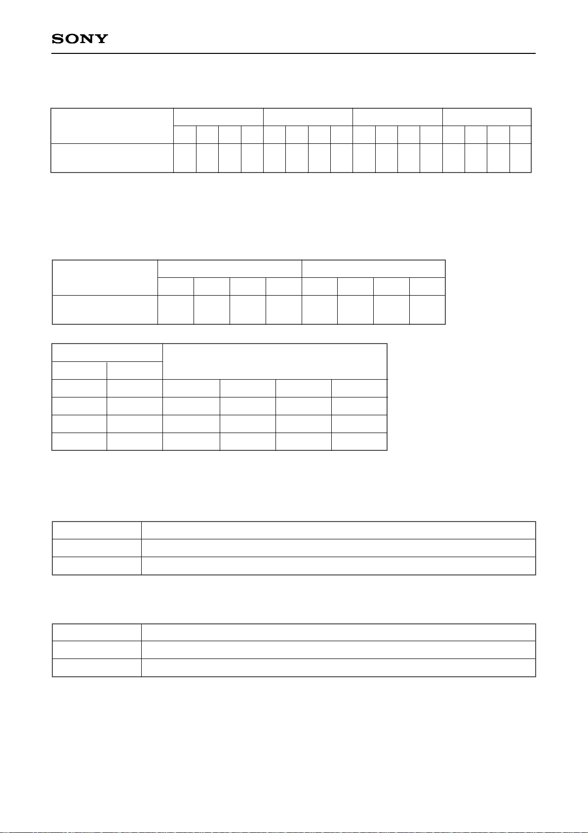
– 74 –
CXD3029R
$BX commands
This command sets the traverse monitor count.
Command
Data 1
Data 2
Data 3
Data 4
D3 D2 D1 D0 D3 D2 D1 D0 D3 D2 D1 D0 D3 D2 D1 D0
2
15
2
14
2132122112102928272625242322212
0
Traverse monitor
count setting
• When the set number of tracks are counted during fine search, the sled control for the traverse cycle control
goes off.
• The traverse monitor count is set to monitor the traverse status using the SENS outputs COMP and COUT.
Command bit
MTSL1 MTSL0
Output data
XUGF
MINT0
RFCK
C4M
XPCK
MNT1
XPCK
FSTO
GFS
MNT2
XROF
GFS
C2PO
MNT3
GTOP
C2PO
0
0
1
1
0
1
0
1
Command
Data 5
Traverse monitor
count setting
0 0 MTSL1 MTSL0
D3 D2 D1 D0
Data 6
ASYE MD2 0 0
D3 D2 D1 D0
The monitor output is set as follows.
Command bit
ASYE = 1
ASYE = 0
Asymmetry is on.
Asymmetry is off.
Processing
Command bit
MD2 = 0
MD2 = 1
Digital Out on/off control. Off when "0".
Digital Out on/off control. On when "1".
Processing
∗
However, the $39 command SRO1 and $A7 command MON SEL must be set to "0".
∗
∗: preset
∗
∗: preset
∗
∗: preset
Page 75

– 75 –
CXD3029R
Spindle servo
coefficient setting
CLV CTRL ($DX)
Gain
MDP1
Gain
MDP0
Gain
MDS1
Gain
MDS0
Gain
CLVS
Gain
MDS1
0
0
0
0
1
1
Gain
MDS0
0
0
1
1
0
0
Gain
CLVS
0
1
0
1
0
1
GCLVS
–12dB
–6dB
–6dB
0dB
0dB
+6dB
Command
D3
Data 1
D2
D1
D0
Gain
DCLV0
Gain
DCLV1
PCC1
PCC0
D3
Data 2
D2
D1
D0
$CX commands
• CLVS mode gain setting: GCLVS
Gain
MDP1
0
0
1
Gain
MDP0
0
1
0
GMDP
–6dB
0dB
+6dB
Gain
DCLV1
0
0
1
Gain
DCLV0
0
1
0
GDCLV
0dB
+6dB
+12dB
Gain
MDS1
0
0
1
Gain
MDS0
0
1
0
GMDS
–6dB
0dB
+6dB
• CLVP mode gain setting: GMDP: GMDS
• DCLV overall gain setting: GDCLV
Command bit
PCC1 PCC0
Processing
The VPCO signal is output.
The VPCO pin output is high impedance.
The VPCO pin output is low.
The VPCO pin output is high.
0
0
1
1
0
1
0
1
• This command controls the VPCO pin signal.
The VPCO output can be controlled with this setting.
Page 76

– 76 –
CXD3029R
Command
Data 3
D3
SFP3 SFP2 SFP1 SFP0 SRP3 SRP2 SRP1 SRP0
Spindle servo
coefficient setting
D2 D1 D0 D3 D2 D1 D0
Data 4
Command
Data 5
D3
EDC7 EDC6 EDC5 EDC4 EDC3 EDC2 EDC1 EDC0
Spindle servo
coefficient setting
D2 D1 D0 D3 D2 D1 D0
Data 6
∗
See "§4-2. Frame Sync Protection" regarding frame sync protection.
Command bit
SRP3 to SRP0
Sets the number of frame sync backward protection times. The setting range is from 1 to F (h).
Processing
Command bit
SFP3 to SFP0
Sets the number of frame sync forward protection times. The setting range is from 1 to F (h).
Processing
• The CXD3029R can serially output the 40 bits (10 BCD codes) of error rate data selected by EDC7 to EDC0
from the SQSO pin and monitor this data using a microcomputer.
In order to output error rate data, set $C commands for C1 and C2 individually, and set $8 commands
SOCT0 and SOCT1 to "1". Then, the data can be read out from the SQSO pin by sending 40 SQCK pulses.
Preset value: 00h
Page 77

– 77 –
CXD3029R
Command
Data 2
CLV CTRL VP7 VP6 VP5 VP4
D3 D2 D1 D0
Data 3
VP3 VP2 VP1 VP0
D3 D2 D1 D0
Data 4
VP
CTL1VPCTL0
00
D3 D2 D1 D0
$DX commands
See "$CX commands".
Command bit
TB = 0
TB = 1
TP = 0
TP = 1
Bottom hold at a cycle of RFCK/32 in CLVS mode.
Bottom hold at a cycle of RFCK/16 in CLVS mode.
Peak hold at a cycle of RFCK/4 in CLVS mode.
Peak hold at a cycle of RFCK/2 in CLVS mode.
Description
Command
Data 1
CLV CTRL 0 TB TP
Gain
CLVS
D3 D2 D1 D0
Command bit
EDC7 = 0 EDC6
EDC5
EDC4
EDC3
EDC2
EDC1
EDC0
EDC7 = 1 EDC6
EDC5
EDC4
EDC3
EDC2
EDC1
EDC0
The [No C1 errors, pointer reset] count is output When "1".
The [One C1 error corrected, pointer reset] count is output When "1".
The [No C1 errors, pointer set] count is output When "1".
The [One C1 error corrected, pointer set] count is output When "1".
The [Two C1 errors corrected, pointer set] count is output When "1".
The [C1 correction impossible, pointer set] count is output When "1".
7350-frame count cycle mode
∗
1
When "0".
73500-frame count cycle mode∗2When "1".
The [No C2 errors, pointer reset] count is output When "1".
The [One C2 error corrected, pointer reset] count is output When "1".
The [Two C2 errors corrected, pointer reset] count is output When "1".
The [Three C2 errors corrected, pointer reset] count is output When "1".
The [Four C2 errors corrected, pointer reset] count is output When "1".
The [C2 correction impossible, pointer copy] count is output When "1".
The [C2 correction impossible, pointer set] count is output When "1".
Processing
Error rate monitor commands
∗
1
The values selected by C1 (EDC1 to EDC6) and C2 (EDC0 to EDC6) are added to C1 and C2, respectively,
and output every 7350 frames.
∗2
The values selected by C1 (EDC1 to EDC6) and C2 (EDC0 to EDC6) are added to C1 and C2, respectively,
and output every 73500 frames.
Page 78

– 78 –
CXD3029R
The rotational velocity R of the spindle can be expressed with the following equation.
R = × l
256 – n
32
∗
The above setting should be "0", "0" except for the CAV-W operating mode.
Command bit
VPCTL1 VPCTL0
Processing
The setting of VP0 to VP7 is multiplied by 1.
The setting of VP0 to VP7 is multiplied by 2.
The setting of VP0 to VP7 is multiplied by 3.
The setting of VP0 to VP7 is multiplied by 4.
0
0
1
1
0
1
0
1
Command bit
Processing
VP0 to VP7
Sets the spindle rotational velocity.
R: Relative velocity at normal speed = 1
n: VP0 to VP7 setting value
l: Multiple set by VPCTL0, VPCTL1
Command bit
VP0 to VP7 = F0 (h)
:
VP0 to VP7 = E0 (h)
:
VP0 to VP7 = C0 (h)
Playback at half (normal) speed
to
Playback at normal (double) speed
to
Playback at (quadruple) speed
Description
Notes) 1. Values when crystal is 16.9344MHz and XTSL is low or when crystal is 33.8688MHz and XTSL is high.
2. Values in parentheses are for when DSPB is "1".
F0 E0
0.5
1
1.5
2
R – Relative velocity [multiple]
VP0 to VP7 setting value [h]
D0
2.5
3
C0
3.5
4
DSPB = 0
DSPB = 1
The settings in CAV-W mode are as follows.
Page 79

– 79 –
CXD3029R
Command bit
Processing
VPCTL1 to VPCTL0,
VP7 to VP0
Sets the pitch for variable pitch mode.
The settings in variable pitch mode are as follows.
The pitch setting can be expressed with the following equation.
P = [%]
–n
10
P: Pitch setting value
n: VPCTL1 and VPCTL0, VP7 to VP0 setting value (two's complement,
VPCTL1 = sign bit)
The pitch setting range is from –48.7 to +51.2%.
The plus pitch setting should not exceed the playback speed given in the Recommended Operating Conditions.
An example of variable pitch mode commands is shown below.
$EX001 (Sets INV VPCO = 1.)
$AE4 (Setting to enable variable pitch mode.)
$AEC (Turns on variable pitch mode. The internal clock uses the VCO2 reference.)
$D60A00 (Sets the pitch to –1.0%.)
$D60000 (Sets the pitch to 0.0%.)
$AE4 (Turns off variable pitch mode. The internal clock uses the crystal reference.)
VPCTL1
1
1
0
0
VPCTL0
0
1
0
1
VP7 to VP0
00 (H)
:
FF (H)
00 (H)
:
FF (H)
00 (H)
:
FF (H)
00 (H)
:
E7 (H)
Pitch setting value [%]
+51.2
to
+25.7
+25.6
to
+0.1
0.0
to
–25.5
–25.6
to
–48.7
Command setting example
$D60080
:
$D6FF80
$D600C0
:
$D6FFC0
$D60000
:
$D6FF00
$D60040
:
$D6E740
Command bit
Page 80

– 80 –
CXD3029R
$EX commands
Command
Data 1
SPD mode CM3 CM2 CM1 CM0
D3 D2 D1 D0
Data 2
EPWM SPDC ICAP SFSL
D3 D2 D1 D0
Data 3
VC2C HIFC LPWR VPON
D3 D2 D1 D0
Command bit
CM3 CM2 CM1
Description
Spindle stop mode.
∗
1
Spindle forward rotation mode.
∗1
Spindle reverse rotation mode. Valid only when LPWR = 0
in any mode.
∗1
Rough servo mode. When the RF-PLL circuit isn't locked,
this mode is used to pull the disc rotations within the RFPLL capture range.
PLL servo mode.
Automatic CLVS/CLVP switching mode.
Used for normal playback.
0
1
1
1
1
0
0
0
0
1
1
1
0
0
1
1
1
1
CM0
0
0
0
0
1
0
Mode
STOP
KICK
BRAKE
CLVS
CLVP
CLVA
∗
1
See Timing Charts 1-6 to 1-29.
In the digital CLV servo, the sampling frequency of the internal digital filter is switched simultaneously with
the switching of CLVP/CLVS.
Then, the CLVS mode cut-off frequency fc is 70Hz when $D command TB = 0 or 140Hz when $D command
TB = 1.
Spindle control can be set to the ternary output of only MDP or the binary outputs of MDP and MDS by $AF
commands MDPOUTSL1 and MDPOUTSL0.
Command bit
EPWM SPDC ICAP
Description
Crystal reference CLV servo.
VCO2 reference CLV servo.
Used for playback in CLV-W
mode.
∗2
Spindle control with VP0 to VP7.
Spindle control with the external
PWM.
VCO control
∗3
0
0
0
0
1
0
0
0
0
1
0
0
0
0
0
1
1
0
SFSL
0
0
0
0
0
0
VC2C
0
0
1
0
0
0
HIFC
0
0
1
1
1
1
LPWR
0
0
0
0
0
0
VPON
0
0
0
1
1
1
INV
VPCO
0
1
0
0
0
1
Mode
CLV-N
CLV-N
CLV-W
CAV-W
CAV-W
VCO-C
∗
2
Figs. 3-1 and 3-2 show the control flow with the microcomputer software in CLV-W mode.
∗3
Fig. 3-3 shows the control flow with the microcomputer software in VCO-C mode.
Page 81

– 81 –
CXD3029R
Mode
CLV-N
CLV-W
CAV-W
LPWR
0
0
1
0
1
Command
KICK
BRAKE
STOP
KICK
BRAKE
STOP
KICK
BRAKE
STOP
KICK
BRAKE
STOP
KICK
BRAKE
STOP
1-6 (a)
1-6 (b)
1-6 (c)
1-7 (a)
1-7 (b)
1-7 (c)
1-8 (a)
1-8 (b)
1-8 (c)
1-9 (a)
1-9 (b)
1-9 (c)
1-10 (a)
1-10 (b)
1-10 (c)
Timing chart –
Ternary output
Mode
CLV-N
CLV-W
CAV-W
LPWR
0
0
1
0
1
0
1
LPWR2
0
0
0
1-11
1-12
1-13
1-14 (EPWM = 0)
1-15 (EPWM = 0)
1-16 (EPWM = 1)
1-17 (EPWM = 1)
Timing chart –
Ternary output
1-18 (a)
1-18 (b)
1-18 (c)
1-19 (a)
1-19 (b)
1-19 (c)
1-20 (a)
1-20 (b)
1-20 (c)
1-21 (a)
1-21 (b)
1-21 (c)
1-22 (a)
1-22 (b)
1-22 (c)
Timing chart –
Binary output
0
0
0
0
0
LPWR2
1-23
1-24
1-25
1-26 (EPWM = 0)
1-27 (EPWM = 0)
1-28 (EPWM = 1)
1-29 (EPWM = 1)
Timing chart –
Binary output
Page 82

– 82 –
CXD3029R
Command
SPD mode
Data 4
• This sets the gain when controlling the spindle with VP7 to VP0
in CAV-W mode.
Note) The Gain CAV1 and Gain CAV0 commands are invalid for
spindle control with the external PWM.
D3
D2 D1 D0
Gain
CAV1
Gain
CAV0
0
INV
VPCO
Gain
CAV1
0
0
1
1
Gain
CAV0
0
1
0
1
Gain
0dB
–6dB
–12dB
–18dB
See page 80.
Mode
CLV-W
CAV-W
LPWR
0
1
0
1
Command
KICK
BRAKE
STOP
KICK
BRAKE
STOP
KICK
BRAKE
STOP
KICK
BRAKE
STOP
1-8 (a)
1-8 (b)
1-8 (c)
1-8 (a)
1-8 (b)
1-8 (c)
1-10 (a)
1-10 (b)
1-10 (c)
1-10 (a)
1-10 (b)
1-10 (c)
Timing chart –
Ternary output
1-30 (a)
1-30 (b)
1-30 (c)
1-31 (a)
1-31 (b)
1-31 (c)
1-32 (a)
1-32 (b)
1-32 (c)
1-33 (a)
1-33 (b)
1-33 (c)
Timing chart –
Binary output
1
1
1
1
LPWR2
Mode
CLV-W
CAV-W
LPWR
0
1
0
1
0
1
LPWR2
1
1
1-13
1-13
1-15 (EPWM = 0)
1-15 (EPWM = 0)
1-17 (EPWM = 1)
1-17 (EPWM = 1)
Timing chart –
Ternary output
1-34
1-35
1-36 (EPWM = 0)
1-37 (EPWM = 0)
1-38 (EPWM = 1)
1-39 (EPWM = 1)
Timing chart –
Binary output
Page 83

– 83 –
CXD3029R
Timing Chart 1-3
Rch 16-bit C2 Pointer Lch 16-bit C2 Pointer
If C2 Pointer = 1,
data is NG
C2 Pointer for upper 8 bits C2 Pointer for lower 8 bits
Rch C2 Pointer
C2 Pointer for upper 8 bits
C2 Pointer for lower 8 bits
Lch C2 Pointer
LRCK
WDCK
CDROM = 0
C2PO
CDROM = 1
C2PO
48 bit slot
Page 84

– 84 –
CXD3029R
Timing Chart 1-4
Level Meter Timing
96 clock pulses
WFCK
123
96 clock pulses
CRCF CRCF
123
Peak data of this section
16 bits
R/LL/R
96-bit data
Hold section
123 8081 96
CRCF
SQCK
D0 D1 D2 D3 D4 D5 D6 D13 D14 L/R
Peak data
L/R flag
Subcode Q data
See "Subcode Interface"
15-bit peak data
Absolute value display, LSB first
750ns to 120µs
SQCK
SQSO
SQSO
Page 85

– 85 –
CXD3029R
Timing Chart 1-5
Measurement
Peak Meter Timing
96 clock pulses
CRCF
WFCK
123
Measurement Measurement
96 clock pulses
CRCF CRCF
123
SQCK
Page 86

– 86 –
CXD3029R
Ternary output from MDP pin ($AF MDPOUTSL1 = 0, MDPOUTSL0 = 0)
Timing Chart 1-6
CLV-N mode LPWR = 0, LPWR2 = 0
KICK
MDP
H
(a) KICK
BRAKE
MDP
(b) BRAKE
STOP
MDP
(c) STOP
Z
Z
L
Z
Timing Chart 1-7
CLV-W mode (when following the spindle rotational velocity) LPWR = 0, LPWR2 = 0
KICK
MDP
H
(a) KICK
BRAKE
MDP
(b) BRAKE
STOP
MDP
(c) STOP
Z
Z
L
Z
Timing Chart 1-8
CLV-W mode (when following the spindle rotational velocity) LPWR = 1, LPWR2 = 0
KICK
MDP
H
(a) KICK
BRAKE
MDP
(b) BRAKE
Z
STOP
MDP
(c) STOP
Z
Z
Timing Chart 1-9
CAV-W mode LPWR = 0, LPWR2 = 0
KICK
MDP
H
(a) KICK
BRAKE
MDP
(b) BRAKE
STOP
MDP
(c) STOP
Z
L
Timing Chart 1-10
CAV-W mode LPWR = 1, LPWR2 = 0
KICK
MDP
H
(a) KICK
BRAKE
MDP
(b) BRAKE
Z
STOP
MDP
(c) STOP
Z
Page 87

– 87 –
CXD3029R
Timing Chart 1-14
CAV-W mode EPWM = LPWR = 0, LPWR2 = 0
MDP
Acceleration
Z
Deceleration
264kHz
3.8µs
Timing Chart 1-11
CLV-N mode LPWR = 0, LPWR2 = 0
MDP
Acceleration
Z
Deceleration
132kHz
7.6µs
n • 236 (ns) n = 0 to 31
Timing Chart 1-12
CLV-W mode LPWR = 0, LPWR2 = 0
MDP
Acceleration
Z
Deceleration
264kHz
3.8µs
Timing Chart 1-13
CLV-W mode LPWR = 1, LPWR2 = 0
MDP
Acceleration
Z
264kHz
3.8µs
The BRAKE pulse is masked when LPWR = 1.
Timing Chart 1-15
CAV-W mode EPWM = 0, LPWR = 1, LPWR2 = 0
MDP
Acceleration
Z
264kHz
3.8µs
The BRAKE pulse is masked when LPWR = 1.
Page 88
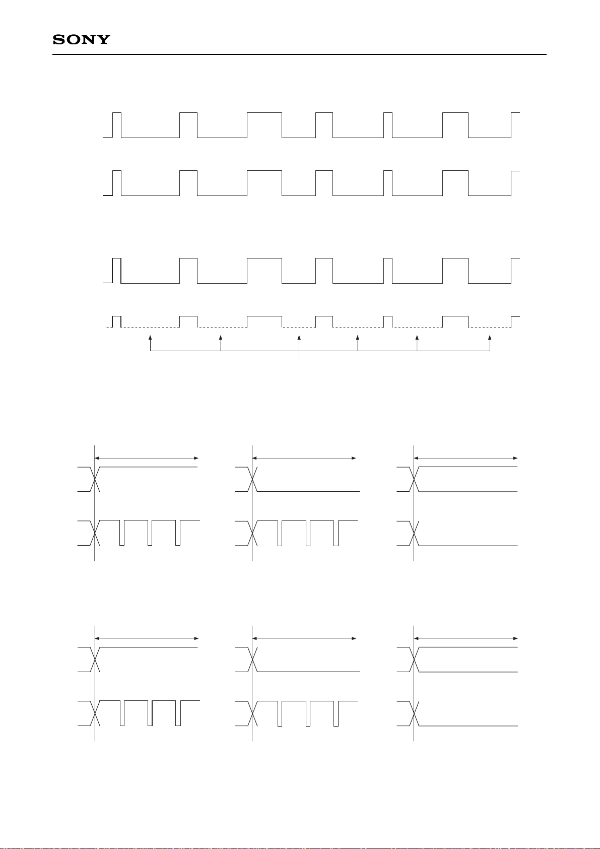
– 88 –
CXD3029R
Timing Chart 1-16
CAV-W mode EPWM = 1, LPWR = 0, LPWR2 = 0
PWMI
MDP
H
L
H
L
Acceleration
Deceleration
Timing Chart 1-17
CAV-W mode EPWM = LPWR = 1, LPWR2 = 0
PWMI
MDP
H
L
H
Z
Acceleration
The BRAKE pulse is masked when LPWR = 1.
Binary output from MDP and MDS pins ($AF MDPOUTSL1 = 1, MDPOUTSL0 = 0)
Timing Chart 1-18
CLV-N mode LPWR = 0, LPWR2 = 0
KICK
MDS
MDP
H
(a) KICK
BRAKE
MDS
MDP
(b) BRAKE
STOP
MDS
MDP
(c) STOP
L
H
L
L
L
H
Timing Chart 1-19
CLV-W mode (when following the spindle rotational velocity) LPWR = 0, LPWR2 = 0
KICK
MDS
MDP
H
(a) KICK
BRAKE
MDS
MDP
(b) BRAKE
STOP
MDS
MDP
(c) STOP
L
H
L
L
L
H
Page 89

– 89 –
CXD3029R
Timing Chart 1-20
CLV-W mode (when following the spindle rotational velocity) LPWR = 1, LPWR2 = 0
KICK
MDS
MDP
H
BRAKE
MDS
MDP
STOP
MDS
MDP
L
LL
H
Timing Chart 1-21
CAV-W mode LPWR = 0, LPWR2 = 0
KICK
MDS
MDP
H
(a) KICK
H
BRAKE
MDS
MDP
(b) BRAKE
STOP
MDS
MDP
(c) STOP
L
L
H
Timing Chart 1-22
CAV-W mode LPWR = 1, LPWR2 = 0
KICK
MDS
MDP
H
(a) KICK
BRAKE
MDS
MDP
(b) BRAKE
STOP
MDS
MDP
(c) STOP
LL
H
Page 90

– 90 –
CXD3029R
Timing Chart 1-23
CLV-N mode LPWR = 0, LPWR2 = 0
MDS
MDP
Acceleration Deceleration
132kHz
7.6µs
n • 236 (ns) n = 0 to 31
Output waveforms with DCLV = 1
L
H
Timing Chart 1-24
CLV-W mode LPWR = 0, LPWR2 = 0
MDS
MDP
Acceleration
L
Deceleration
264kHz
3.8µs
Output waveforms with DCLV = 1
L
Timing Chart 1-25
CLV-W mode LPWR = 1, LPWR2 = 0
MDS
MDP
Acceleration
L
264kHz
3.8µs
Output waveforms with DCLV = 1
The BRAKE pulse is masked when LPWR = 1.
H
Timing Chart 1-26
CAV-W mode EPWM = 0, LPWR = 0, LPWR2 = 0
MDP
Acceleration
L
Deceleration
264kHz
3.8µs
MDS
L
Page 91

– 91 –
CXD3029R
Timing Chart 1-27
CAV-W mode EPWM = 0, LPWR=1, LPWR2 = 0
MDP
Acceleration
L
264kHz
3.8µs
The BRAKE pulse is masked when LPWR = 1.
MDS
H
Timing Chart 1-28
CAV-W mode EPWM = 1, LPWR = 0, LPWR2 = 0
PWMI
MDP
H
L
H
L
Acceleration
Deceleration
MDS
H
Timing Chart 1-29
CAV-W mode EPWM = 1, LPWR = 1, LPWR2 = 0
PWMI
H
L
MDP
H
Acceleration
MDS
H
Page 92
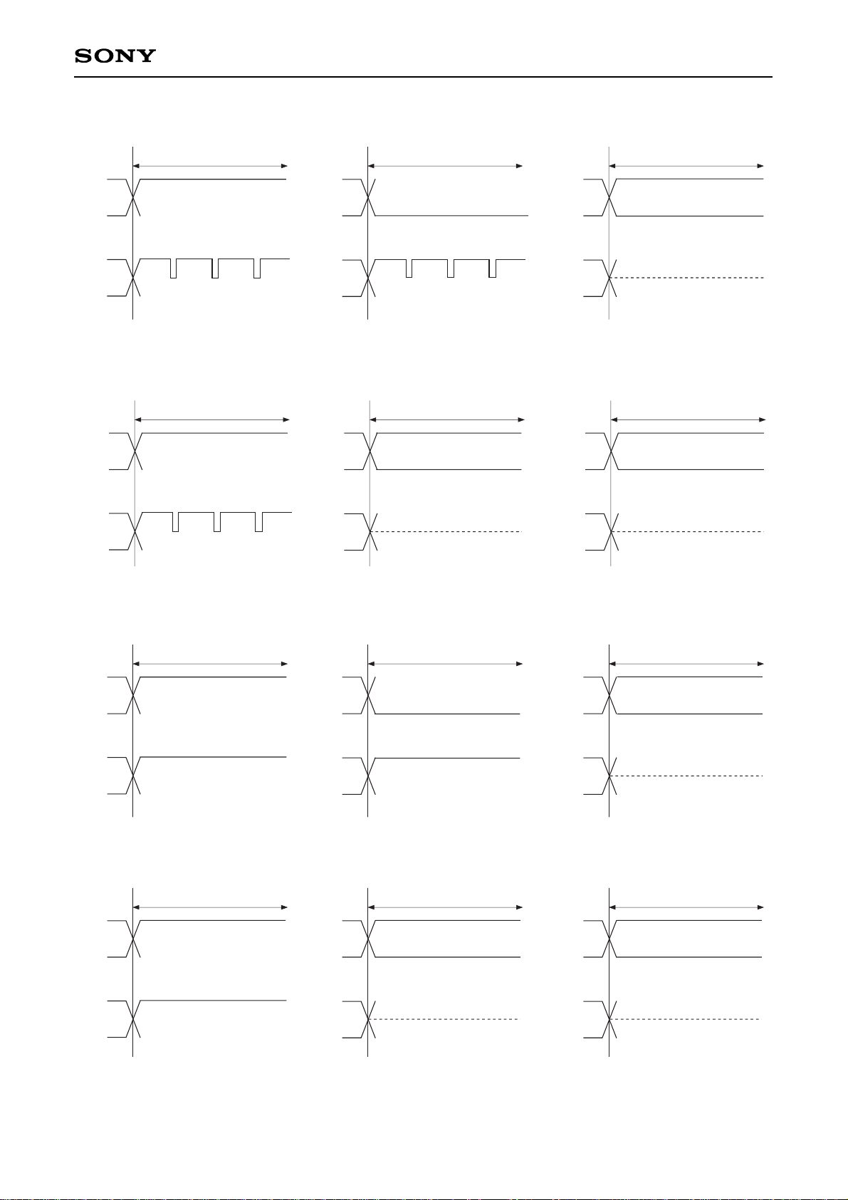
– 92 –
CXD3029R
Timing Chart 1-30
CLV-W mode (when following the spindle rotational velocity) LPWR = 0, LPWR2 = 1
KICK
MDS
MDP
H
(a) KICK
BRAKE
MDS
MDP
(b) BRAKE
STOP
MDS
MDP
(c) STOP
Z
H
Z
L
Z
H
Timing Chart 1-31
CLV-W mode (when following the spindle rotational velocity) LPWR = 1, LPWR2 = 1
KICK
MDS
MDP
H
BRAKE
MDS
MDP
STOP
MDS
MDP
Z
Z
Z
H
(a) KICK (b) BRAKE (c) STOP
Timing Chart 1-32
CAV-W mode LPWR = 0, LPWR2 = 1
KICK
MDS
MDP
H
(a) KICK
H
BRAKE
MDS
MDP
(b) BRAKE
STOP
MDS
MDP
(c) STOP
Z
L
H
Timing Chart 1-33
CAV-W mode LPWR = 1, LPWR2 = 1
KICK
MDS
MDP
H
(a) KICK
BRAKE
MDS
MDP
(b) BRAKE
STOP
MDS
MDP
(c) STOP
ZZ
H
Page 93

– 93 –
CXD3029R
Timing Chart 1-34
CLV-W mode LPWR = 0, LPWR2 = 1
MDS
MDP
Acceleration
Z
Deceleration
264kHz
3.8µs
Output waveforms with DCLV = 1
Timing Chart 1-35
CLV-W mode LPWR = 1, LPWR2 = 1
MDS
MDP
Acceleration
Z
264kHz
3.8µs
Output waveforms with DCLV = 1
The BRAKE pulse is masked when LPWR = 1.
H
Timing Chart 1-36
CAV-W mode EPWM = 0, LPWR = 0, LPWR2 = 1
MDP
Acceleration
Z
Deceleration
264kHz
3.8µs
MDS
L
Page 94

– 94 –
CXD3029R
Timing Chart 1-37
CAV-W mode EPWM = 0, LPWR=1, LPWR2 = 1
MDP
Acceleration
Z
264kHz
3.8µs
The BRAKE pulse is masked when LPWR = 1.
MDS
H
Timing Chart 1-38
CAV-W mode EPWM = 1, LPWR = 0, LPWR2 = 1
PWMI
MDP
H
L
H
L
Acceleration
Deceleration
MDS
H
Timing Chart 1-39
CAV-W mode EPWM = 1, LPWR = 1, LPWR2 = 1
PWMI
H
L
MDP
H
Acceleration
MDS
H
Z
Page 95

– 95 –
CXD3029R
[2] Subcode Interface
There are two methods for reading out a subcode externally.
The 8-bit subcodes P to W can be read out from SBSO by inputting EXCK.
The subcode-Q can be read out after checking CRC of the 80 bits in the subcode frame.
The subcode-Q can be read out from the SQSO pin by inputting 80 clock pulses to the SQCK pin when SCOR
comes correctly and CRCF is high.
§2-1. P to W Subcode Readout
Data can be read out by inputting EXCK immediately after WFCK falls. (See Timing Chart 2-1.)
§2-2. 80-bit Subcode-Q Readout
Fig. 2-2 shows the peripheral block of the 80-bit subcode-Q register.
• First, subcode-Q, regenerated at one bit per frame, is input to the 80-bit serial/parallel register and the CRC
check circuit.
• 96-bit subcode-Q is input, and if the CRC is OK, it is output to SQSO with CRCF = 1. In addition, 80 bits are
loaded into the parallel/serial register.
When SQSO goes high after SCOR is output, the CPU determines that new data (which passed the CRC
check) has been loaded.
• When the 80-bit data is loaded, the order of the MSB and LSB is inverted within each byte. As a result,
although the sequence of the bytes is the same, the bits within the bytes are now ordered LSB first.
• Once the 80-bit data load is confirmed, SQCK is input so that the data can be read.
The SQCK input is detected, and the retriggerable monostable multivibrator is reset while the input is low.
• The retriggerable monostable multivibrator has a time constant from 270 to 400µs. When the duration when
SQCK is high is less than this time constant, the monostable multivibrator is kept reset; during this interval,
the serial/parallel register is not loaded into the parallel/serial register.
• While the monostable multivibrator is being reset, data cannot be loaded in the peak detection parallel/serial
register or the 80-bit parallel/serial register.
In other words, while reading out with a clock cycle shorter than this time constant, these registers will not be
rewritten by CRCOK and others.
• The previously mentioned peak detection register can be connected to the shift-in of the 80-bit parallel/serial
register.
For ring control 1, input and output are shorted during peak meter and level meter modes.
For ring control 2, input and output are shorted during peak meter mode.
This is because the register is reset with each readout in level meter mode, and to prevent readout
destruction in peak meter mode.
As a result, the 96-bit clock must be input in peak meter mode.
• The absolute time after peak is stored in the memory in peak meter mode as noted in "Description of peak
meter mode" on page 95. See Timing Chart 2-3.
• The clock is input from the SQCK pin to perform these operations. The high and low intervals of the clock
should be between 750ns and 120µs.
Page 96

– 96 –
CXD3029R
Timing Chart 2-1
Internal
PLL clock
4.3218 ± ∆MHz
WFCK
SCOR
EXCK
SBSO
750ns max
S0
• S1 Q R
WFCK
SCOR
EXCK
SBSO
S0•S1 Q R S T U V W
S0•S1
P1 Q R S T U V W P1 P2 P3
Same Same
Subcode P.Q.R.S.T.U.V.W Read Timing
Page 97

– 97 –
CXD3029R
Block Diagram 2-2
888888888
Order
inversion
16
Peak detection
LOAD CONTROL
Ring control 2
CRCF
Mix
Monostable
multivibrator
CRCC
ABS time load control
for peak value
16-bit P/S register
Ring control 1
SO SI
SQSO
SQCKSHIFTSHIFT
SUBQ
LD
LD
LD
LD
LD
LD
LD
LD
SO
HGFEDCBA
ABCDEFGH
SI
80-bit P/S Register
80-bit S/P Register
(AFRAM) (ASEC) (AMIN) ADDRS CTRL
SIN
SUBQ
Page 98
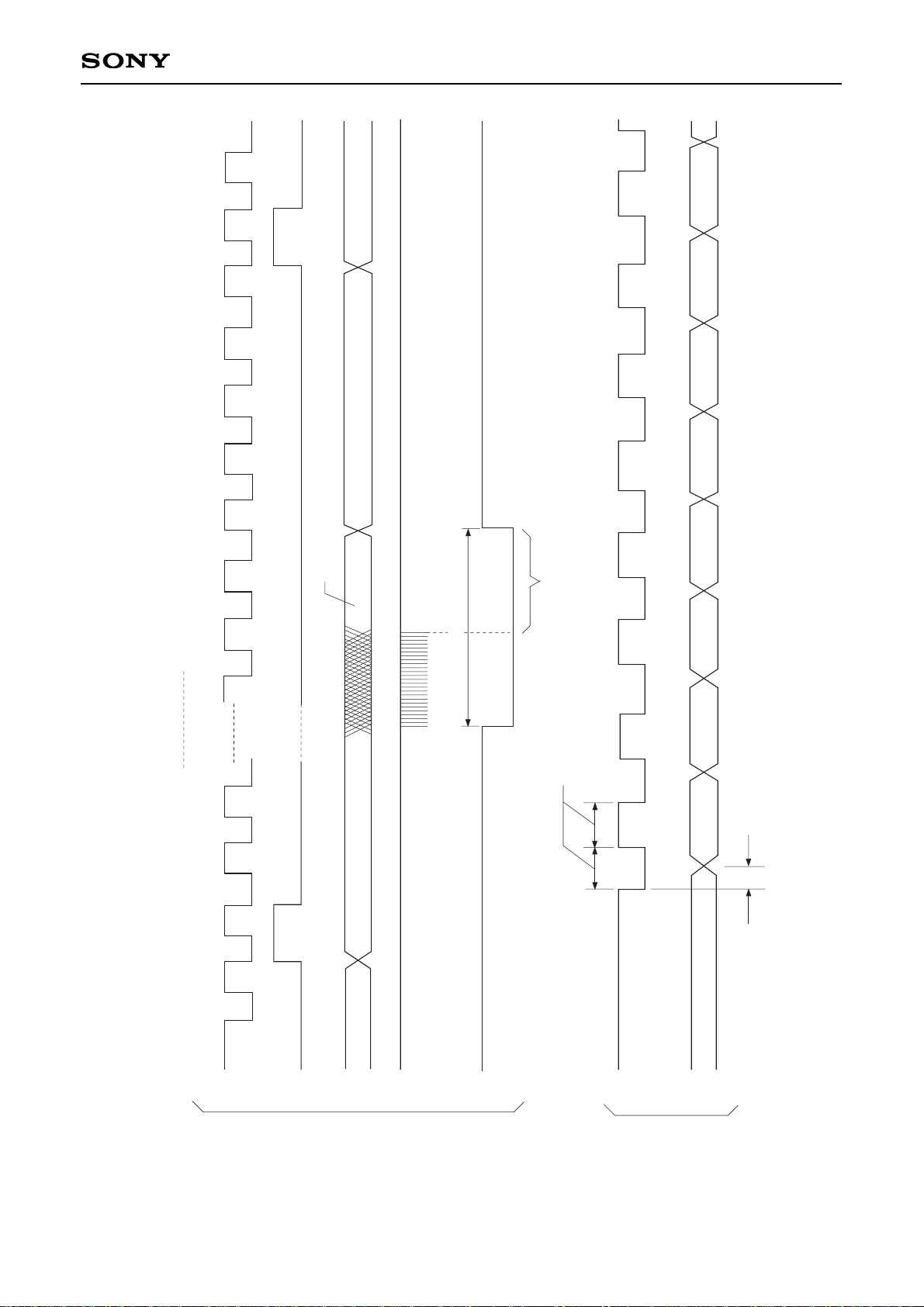
– 98 –
CXD3029R
Timing Chart 2-3
1
2
3
91 92 93 94
95 96 97
98
WFCK
SCOR
SQSO
SQCK
Monostable
multivibrator
(Internal)
CRCF1
Determined by mode
CRCF2
80 or 96 clocks
Register load forbidder
270 to 400µs when SQCK = high.
750ns to 120µs
300ns max
CRCF
ADR0
ADR1
ADR2
ADR3
CTL0
CTL1
CTL2
CTL3
SQCK
SQSO
1
2
3
CRCF1
Page 99

– 99 –
CXD3029R
Timing Chart 2-4
Example: $802000 latch
Set SQCK high during this interval.
Internal signal latch
PER0 PER1 PER2 PER3 PER4 PER5 PER6 PER7 C1F0 C1F1 C1F2 C2F0 C2F1 C2F2 FOK GFS LOCK EMPH
750ns or more
XLAT
SQCK
SQSO
ALOCK
VF0 VF1 VF2 VF3 VF4 VF5 VF6 VF9VF7 VF8
Signal
PER0 to PER7
FOK
GFS
LOCK
EMPH
ALOCK
VF0 to VF9
RF jitter amount (used to adjust the focus bias). 8-bit binary data in PER0 = LSB, PER7 = MSB.
Focus OK.
High when the frame sync and the insertion protection timing match.
GFS is sampled at 460Hz; when GFS is high, this pin outputs a high signal. If GFS is low eight consecutive samples, this pin outputs low.
High when the playback disc has emphasis.
GFS is sampled at 460Hz; when GFS is high eight consecutive samples, this pin outputs a high signal. If GFS is low eight consecutive
samples, this pin outputs low.
Used in CAV-W mode. The result obtained by measuring the rotational velocity of the disc. (See Timing Chart 2-5.) VF0 = LSB, VF9 = MSB.
Description
C1F2
0
0
0
0
1
1
1
1
0
0
1
1
0
0
1
1
0
1
0
1
0
1
0
1
No C1 errors; C1 pointer reset
One C1 error corrected; C1 pointer reset
—
—
No C1 errors; C1 pointer set
One C1 error corrected; C1 pointer set
Two C1 errors corrected; C1 pointer set
C1 correction impossible; C1 pointer set
C1F1 C1F0 Description
C2F2
0
0
0
0
1
1
1
1
0
0
1
1
0
0
1
1
0
1
0
1
0
1
0
1
No C2 errors; C2 pointer reset
One C2 error corrected; C2 pointer reset
Two C2 errors corrected; C2 pointer reset
Three C2 errors corrected; C2 pointer reset
Four C2 errors corrected; C2 pointer reset
—
C2 correction impossible; C1 pointer copy
C2 correction impossible; C2 pointer set
C2F1 C2F0 Description
Page 100

– 100 –
CXD3029R
Timing Chart 2-5
Measurement interval (approximately 3.8µs)
Reference window
(132.2kHz)
Measurement pulse
(V16M/2)
Measurement counter
VF0 to VF9
Load
m
The relative velocity of the disc can be obtained with the following equation.
R = (R: Relative velocity, m: Measurement results)
VF0 to VF9 is the result obtained by counting V16M/2 pulses while the reference signal (132.2kHz) generated
from XTAL (XTAI, XTAO) (384Fs) is high. This value is 31 when the disc is rotating at normal speed and 63 when
it is rotating at double speed (when DSPB is low).
m + 1
32
VF0 VF1 VF2 VF3 VF4 VF5 VF6 VF7 VF8 VF9
"H" or "L"
XLAT
SQCK
SQSO
Set SQCK high during this period.
750ns or more
 Loading...