

Page 1

CXD3607R
Timing Generator for Progressive Scan CCD Image Sensor
Description
The CXD3607R is a timing generator IC which
generates the timing pulses required by Progressive
Scan CCD image sensors as well as signal processing
circuits.
Features
• Base oscillation frequency 57.3MHz
• High-speed/low-speed shutter function
• Supports FINE and DRAFT mode drive
(15 frames/s, 60 frames/s possible)
• Random trigger shutter function
(Supports TRIG and TRIGOUT mode drive)
• Horizontal driver for CCD image sensor
• Vertical driver for CCD image sensor
Applications
Progressive scan CCD cameras
Structure
Silicon gate CMOS IC
Absolute Maximum Ratings
• Supply voltage VDDa, b Vss – 0.3 to +7.0 V
• Input voltage VI Vss – 0.3 to VDD + 0.3 V
• Output voltage VO1 Vss – 0.3 to VDD + 0.3 V
• Operating temperature
• Storage temperature
48 pin LQFP (Plastic)
VL –10.0 to Vss V
VH VL – 0.3 to +26.0 V
VO2 VL – 0.3 to Vss + 0.3 V
VO3 VL – 0.3 to VH + 0.3 V
Topr –20 to +75 °C
Tstg –55 to +150 °C
Applicable CCD Image Sensors
ICX285 (Type 2/3, 1450K pixels)
Sony reserves the right to change products and specifications without prior notice. This information does not convey any license by
any implication or otherwise under any patents or other right. Application circuits shown, if any, are typical examples illustrating the
operation of the devices. Sony cannot assume responsibility for any problems arising out of the use of these circuits.
Recommended Operating Conditions
• Supply voltage VDDa 4.75 to 5.25 V
VDDb 3.0 to 3.6 V
VM 0.0 V
VH 14.55 to 15.45 V
VL –7.5 to –6.5 V
• Operating temperature
Topr –20 to +75 °C
– 1 –
E01318-PS
Page 2

Block Diagram
CXD3607R
OSCI
OSCO
CKI
CKO
MCKO
SSI
SCK
SEN
VD
HD
TRIG
27
26
25
23
22
29
30
31
32
33
34
XSHD
16
XSHP
17
Register
XCPDM
19 20 21
18
1/2
XCPOB
PBLK
1
ADCLKRGV
10
SS
11 12
Pulse Generator
H1
V Driver
13
H2
14
1
DD
V
15
28
24
36
38
39
40
42
47
48
37
41
45
VDD2
DD
3
V
V
DD
4
SS
2
V
SS
3
V
1
SS
4
V
V1
V4
V2A
V2B
V3
SUB
V
M
V
H
V
L
2
RST
378
SYNSL
9
TEST1
TEST2
– 2 –
35
WEN
Page 3

Pin Configuration (Top View)
CXD3607R
V
V1
V4
V2A
V
V2B
NC
NC
V
NC
V3
SUB
29
SSI
3
DD
V
OSCI
OSCO
262728
25
CKI
24
23
22
21
20
19
18
17
16
15
14
13
V
SS
2
CKO
MCKO
ADCLK
PBLK
XCPOB
XCPDM
XSHP
XSHD
V
DD
2
DD
1
V
H2
3
SS
V
36
M
37
35
WEN
TRIG
HD
VD
323334
31
SEN
SCK
30
38
39
40
H
41
42
43
44
L
45
46
47
48
1 2 3 4 5 6 7 8 9 10 11 12
4
SS
V
RST
SYNSL
NC
NC
NC
4
DD
V
TEST1
TEST2
RG
1
SS
V
H1
∗
Groups of pins enclosed in the figure indicate sections for which power supply separation is possible.
– 3 –
Page 4

Pin Description
CXD3607R
Pin
No.
1
2
3
4
5
6
7
8
9
10
11
12
13
14
15
16
17
18
19
20
21
22
23
24
25
26
27
28
29
30
31
32
33
34
35
Symbol I/O Description
VSS4
RST
SYNSL
NC
NC
NC
VDD4
TEST1
TEST2
RG
VSS1
H1
H2
VDD1
VDD2
XSHD
XSHP
XCPDM
XCPOB
PBLK
ADCLK
MCKO
CKO
VSS2
CKI
OSCO
OSCI
VDD3
SSI
SCK
SEN
VD
HD
TRIG
WEN
GND (GND for common logic block)
—
Internal system reset input. (High: Normal operation, Low: Reset operation)
I
Normally apply reset during power-on.
Control input used to switch sync system. (High: CKI sync, Low: MCKO sync)
I
(Leave open.)
—
(Leave open.)
—
(Leave open.)
—
3.3V power supply. (Power supply for common logic block)
—
IC test pin 1 (Normally fix to GND.)
I
IC test pin 2 (Normally fix to GND.) With pull-down resistor
I
CCD reset gate pulse output.
O
GND (GND for H1 and H2 pins)
—
Horizontal CCD drive clock output.
O
Horizontal CCD drive clock output.
O
5.0V power supply. (Power supply for H1 and H2 pins)
—
3.3V power supply. (Power supply for common logic block)
—
CCD data level sample-and-hold pulse output.
O
CCD precharge level sample-and-hold pulse output.
O
CCD dummy signal clamp pulse output.
O
CCD optical black signal clamp pulse output.
O
Pulse output for horizontal and vertical blanking period pulse cleaning.
O
Clock output for analog/digital conversion IC.
O
System clock output for signal processing IC. (28.6MHz)
O
Inverter output. (57.3MHz)
O
GND (GND for common logic block)
—
Inverter input. (57.3MHz)
I
Inverter output for oscillation. (57.3MHz)
O
Inverter input for oscillation. (57.3MHz)
I
3.3V power supply. (Power supply for common logic block)
—
Serial interface data input for internal mode settings.
I
Serial interface clock input for internal mode settings.
I
Serial interface strobe input for internal mode settings.
I
Vertical sync signal input.
I
Horizontal sync signal input.
I
Trigger pulse input.
I
Memory write timing pulse output.
O
With pull-down resistor
– 4 –
Page 5

CXD3607R
Pin
No.
36
37
38
39
40
41
42
43
44
45
46
47
48
Symbol I/O Description
VSS3
M
V
V1
V4
V2A
VH
V2B
NC
NC
VL
NC
V3
SUB
GND (GND for common logic block)
—
GND (GND for vertical driver)
—
CCD vertical register clock output.
O
CCD vertical register clock output.
O
CCD vertical register clock output.
O
15.0V power supply. (Power supply for vertical driver)
—
CCD vertical register clock output.
O
(Leave open.)
—
(Leave open.)
—
–7.0V power supply. (Power supply for vertical driver)
—
(Leave open.)
—
CCD vertical register clock output.
O
CCD electronic shutter pulse output.
O
– 5 –
Page 6

CXD3607R
Electrical Characteristics
DC Characteristics (Within the recommended operating conditions)
Item
Supply
voltage 1
Supply
voltage 2
Supply
voltage 3
Supply
voltage 4
Supply
voltage 5
Input
voltage 1
Input
∗1, ∗2
voltage 2
Output
voltage 1
Output
voltage 2
VDD1
VDD2 to 4
VH
VM
VL
RST, TEST1,
SSI, SCK, SEN,
∗1
VD, HD, TRIG
SYNSL, TEST2
XCPDM, XCPOB,
PBLK, ADCLK,
WEN
XSHD, XSHP,
CKO
Pins
Symbol
VDDa
VDDb
VH
VM
VL
Vt+
Vt–
Vt+
Vt–
VOH1
VOL1
VOH2
VOL2
Conditions Min. Typ. Max. Unit
Feed current where IOH = –3.3mA
Pull-in current where IOL = 2.4mA
Feed current where IOH = –6.6mA
Pull-in current where IOL = 4.8mA
4.75
3.0
14.55
—
–7.5
0.8VDDb
0.8VDDb
VDDb – 0.8
VDDb – 0.8
5.0
3.3
15.0
0
–7.0
5.25
3.6
15.45
—
–6.5
0.2VDDb
0.2VDDb
0.4
0.4
V
V
V
V
V
V
V
V
V
V
V
V
V
Output
voltage 3
Output
voltage 4
RG, MCKO
H1, H2
VOH3
VOL3
VOH4
VOL4
IOL
Output
current 1
V1, V2A, V2B,
V3, V4
VOM1
VOM2
VOH
Output
current 2
∗1
These input pins are Schmitt trigger inputs, and have a protective diode on the power supply side in the IC.
SUB
IOSL
IOSH
Feed current where IOH = –10.4mA
Pull-in current where IOL = 7.2mA
Feed current where IOH = –22.0mA
Pull-in current where IOL = 14.4mA
V1, V2A, V2B, V3, V4 = –8.25V
V1, V2A, V2B, V3, V4 = –0.25V
V2A, V2B = 0.25V
V2A, V2B = 14.75V
SUB = –8.25V
SUB = 14.75V
VDDb – 0.8
0.4
VDDa – 0.8
0.4
10.0
–5.0
5.0
–7.2
5.4
–4.0
Therefore, they do not support 5V input.
∗2
These input pins are with pull-down resistor in the IC.
Note) This table shows the conditions for 3.3V drive.
V
V
V
V
mA
mA
mA
mA
mA
mA
– 6 –
Page 7

CXD3607R
Inverter I/O Characteristics for Oscillation (Within the recommended operating conditions)
Item Pins
Logical Vth
Input voltage
Output voltage
Feedback
resistor
Oscillator
frequency
OSCI
OSCI
OSCO
OSCI
OSCO
OSCI
OSCO
Symbol
LVth
IH
V
VIL
VOH
VOL
RFB
f
Conditions Min. Typ. Max. Unit
—
—
—
Feed current where IOH = –9mA
Pull-in current where IOL = 9mA
VIN = VDDb or VSS
—
0.7V
V
DDb/2
500k
—
—
—
30
Inverter Input Characteristics for Base Oscillation Clock Duty Adjustment
(Within the recommended operating conditions)
Item Pins
Logical Vth
Input voltage
Input amplitude
CKI
Symbol
LVth
VIH
VIL
VIN
Conditions Min. Typ. Max. Unit
—
—
—
fmax 75MHz sine wave
—
0.7VDDb
—
0.3
DDb
VDDb/2
—
—
—
—
2M
—
VDDb/2
—
—
—
—
—
0.3VDDb
—
VDDb/2
5M
75
—
—
0.3VDDb
—
V
V
V
V
V
Ω
MHz
V
V
V
Vp-p
Note) Input voltage is the input voltage characteristics for direct input from an external source. Input
amplitude is the input amplitude characteristics in the case of input through a capacitor.
Switching Characteristics (VH = 15.0V, VM = GND, VL = –7.0V)
Item
Rise time
Fall time
Output noise
voltage
Symbol
TTLM
TTMH
TTLH
TTML
TTHM
TTHL
VCLH
VCLL
VCMH
VCML
VL to VM
VM to VH
VL to VH
VM to VL
VH to VM
VH to VL
Conditions Min. Typ. Max. Unit
200
200
30
200
200
30
350
350
60
350
350
60
500
500
90
500
500
90
1.0
1.0
1.0
1.0
ns
ns
ns
ns
ns
ns
V
V
V
V
1. The MOS structure of this IC has a low tolerance for static electricity, so full care should be given for
measures to prevent electrostatic discharge.
2. For noise and latch-up countermeasures, be sure to connect a by-pass capacitor (0.1µF or more)
between each power supply pin (VH, VL) and GND.
3. To protect the CCD image sensor, clamp the SUB pin output at VH before input to the CCD image sensor.
See the CCD image sensor data sheet for details.
– 7 –
Page 8

Switching Wa veforms
CXD3607R
V2A, V2B
V1, V3, V4
TTLM
10%
TTLM
10%
TTMH TTHM
90%
10%
90%
90%
90%
10%
90%
90%
TTLH TTHL
90%90%
TTML
10%
TTML
10%
H
V
V
M
V
L
V
M
V
L
V
H
Waveform Noise
SUB
VCLH
10% 10%
VCMH
VCLL
VCML
V
L
V
M
VL
– 8 –
Page 9

AC Characteristics
AC characteristics between the serial interface clocks
CXD3607R
Symbol
ts1
th1
ts2
ts3
SSI
SSI
SCK
SEN
SEN
SSI setup time, activated by the rising edge of SCK
SSI hold time, activated by the rising edge of SCK
SCK setup time, activated by the rising edge of SEN
SEN setup time, activated by the rising edge of SCK
0.2V
DD
b
0.2V
0.8VDDb
0.8VDDb
b
th1ts1
ts2
DD
0.2V
DD
b
ts3
Definition Min. Typ. Max. Unit
Serial interface clock internal loading characteristics
DD
b
0.2V
DD
b
0.8V
DD
b
0.2V
(Within the recommended operating conditions)
20
20
20
20
Example: During FINE mode
ns
ns
ns
ns
HD
V2
SCK
SEN
∗
Be sure to maintain a constantly high SEN logic level from around the falling edge of the HD 8H after the
0.2V
DD
ts1
0.8V
b
DD
b
8H 9H
0.2VDDb
th1
0.8V
DD
b
falling edge of VD to around the 9H falling edge and during that horizontal period.
(Within the recommended operating conditions)
Symbol
ts1
th1
Second SCK clock setup time after the rising edge of SEN,
activated by the falling edge of HD
SEN hold time, activated by the falling edge of 9H HD
Definition Min. Typ. Max. Unit
5
30
– 9 –
ns
µs
Page 10

CXD3607R
Serial interface clock output variation characteristics
The serial interface data “Standby setting” is loaded to the CXD3607R and controlled at the rising edge of the
second SCK clock after the rising edge of SEN.
SEN
0.8VDDb
SCK
Output signal
tpdPULSE
(Within the recommended operating conditions)
Symbol Definition Min. Typ. Max. Unit
tpdPULSE
Output signal delay, activated by the rising edge of the
second SCK clock after the rising edge of SEN
10 ns
100
RST loading characteristics
RST
0.2VDDb
0.2VDDb
tw1
(Within the recommended operating conditions)
Symbol Definition Min. Typ. Max. Unit
tw1
RST pulse width
35
VD, HD and TRIG loading characteristics
DD
b
VD/HD/TRIG
0.2V
DD
b
ts1
th1
0.8V
ns
MCKO
0.2VDDb
0.8VDDb
MCKO load capacitance = 16pF
(Within the recommended operating conditions)
Symbol Definition Min. Typ. Max. Unit
ts1
th1
VD/HD/TRIG setup time, activated by the rising edge of MCKO
VD/HD/TRIG hold time, activated by the rising edge of MCKO
20
5
– 10 –
ns
ns
Page 11

Output variation characteristics
CXD3607R
MCKO
WEN
WEN load capacitance = 10pF
Symbol Definition
tpd1
Time until WEN changes after the rise of MCKO
0.8VDDb
tpd1
(Within the recommended operating conditions)
Min. Typ. Max. Unit
ns–60
– 11 –
Page 12

CXD3607R
Description of Operation
Pulses output from the CXD3607R are controlled mainly by the RST and SYNSL pins and by the serial
interface data.
Control by the RST Pin
System reset is performed by setting the CXD3607R RST pin (Pin 2) low. After reset is canceled, the serial
data block is “XSHP, XSHD logic phase adjustment setting” D0 bit = 1 and all other bits = 0.
In addition, when RST = low, some circuit operations in the IC are stopped as shown in the Pin Status Table
below.
Pin Status Table (RST = low)
Pin No. Symbol I/O status
—
L
ACT
—
—
—
—
—
—
ACT
—
ACT
ACT
—
—
ACT
ACT
H
H
H
ACT
ACT
ACT
—
10
11
12
13
14
15
16
17
18
19
20
21
22
23
24
1
2
3
4
5
6
7
8
9
VSS4
RST
SYNSL
NC
NC
NC
VDD4
TEST1
TEST2
RG
VSS1
H1
H2
VDD1
VDD2
XSHD
XSHP
XCPDM
XCPOB
PBLK
ADCLK
MCKO
CKO
VSS2
Pin No. Symbol I/O status
25
26
27
28
29
30
31
32
33
34
35
36
37
38
39
40
41
42
43
44
45
46
47
48
CKI
OSCO
OSCI
VDD3
SSI
SCK
SEN
VD
HD
TRIG
WEN
VSS3
VM
V1
V4
V2A
VH
V2B
NC
NC
VL
NC
V3
SUB
ACT
ACT
ACT
—
DIS
DIS
DIS
DIS
DIS
DIS
L
—
—
VL
VL
VM
—
VM
—
—
—
—
VM
VL
Note) ACT means that the circuit is operating, and DIS means that loading is stopped.
L indicates a low output level, and H a high output level in the controlled status.
VM and VL indicate the voltage levels applied to VM (Pin 37) and VL (Pin 45), respectively.
– 12 –
Page 13

CXD3607R
Control by the SYNSL Pin
The CXD3607R sync system can be switched by the CXD3607R SYNSL pin (Pin 3).
Low: MCKO sync (Normally use with this system configuration.)
Select this when sync signals VD and HD are generated by the MCKO output of the CXD3607R. The VD
and HD inputs are loaded to the CXD3607R at the rising edge of the MCKO pulse.
High: CKI sync
Select this when sync signals VD and HD are generated by the CKI input of the CXD3607R. The VD and
HD inputs are loaded to the CXD3607R at the rising edge of the CKI pulse, and the two MCKO logic
phases (a) and (b) existing after power-on can be aligned at the initial HD input by resetting the inter nal
clock.
Low: MCKO sync
High: CKI sync High: MCKO reset for CKI sync
CKI
Sync signal
generator block
VD/HD
HD
CKI
MCKO (a)
MCKO (b)
CXD3607R
CKI
MCKO
Sync signal
generator block
VD/HD
CXD3607R
Control by the Serial Interface Data
The CXD3607R loads the serial interface data in the following for mat at the rising edge of the second SCK
clock after the rising edge of SEN.
∗
Make sure that SCK does not stop even while SEN is high.
SD11SSI
SD10 SD9 SD8 SD7 SD6 SD5 SD4 SD3 SD2 SD1 SD0
SCK
SEN
In addition, the data are actually reflected at the following positions.
Data other than the following → Reflected at the falling edge of the HD 8H after the falling
edge of VD.
2. Special drive data “SUB stop setting” → Reflected at the falling edge of the HD 9H after the falling
edge of VD.
4. Shutter data “Shutter SUB setting” → Reflected at the falling edge of the HD 9H after the falling
edge of VD.
5. TRIG data → Reflected at the falling edge of the HD 1H after the falling
edge of TRIG.
(Only when the TRIG function setting is 1: TRIG function
enabled)
6. Other data “Standby setting” → Reflected at the rising edge of the second SCK clock after
the rising edge of SEN.
There are six categories of serial interface data: drive mode data, special drive data, logic phase adjustment
data, shutter data, TRIG data and other data. The details of the data for each category are described below.
∗
After reset is canceled, the serial data block is “XSHP, XSHD logic phase adjustment setting” D0 bit = 1 and
all other bits = 0.
– 13 –
Page 14

CXD3607R
1. Drive mode data
SD11 Description of settings
SD101SD91SD81SD70SD61SD51SD40SD3XSD2D2SD1D1SD0
0
Drive mode setting, TRIG
D0
function setting
2. Special drive data
SD11 Description of settings
SD100SD91SD80SD71SD60SD5XSD4XSD3XSD2XSD1D1SD0
0 SG and SUB stop settings
D0
3. Logic phase adjustment data
SD11 Description of settings
SD10 SD9 SD8
0
01
SD7
SD6
SD5
SD4
SD3
SD2
SD1
SD0
1
1
D1
D0
0
0
D1
D0
0
0
0
0
0
0
0
0
XSHP logic phase adjustment
0
setting
XSHD logic phase adjustment
0
setting
1
0
1
D1
D0
0
0
0
0
ADCLK logic phase adjustment
0
setting
4. Shutter data
SD11 Description of settings
SD10 SD9 SD8 SD7 SD6
0
110
1
1
0
SD5
SD4
SD3
SD2
SD1
SD0
0
D5
D4
D3
D2
D1
D0
Shutter V setting
1
D11
D10
0
D5
D4
D9
D3
D8
D2
D7
D1
D6
D0
Shutter SUB setting
1
D11
D10
D9
D8
D7
D6
5. TRIG data
SD11 Description of settings
SD10 SD9 SD8 SD7 SD61SD5
SD4
SD3
SD2
SD1
SD0
SG and SUB stop settings
0
0
D3
D2
D1
High-speed sweep setting
D0
Clamp pulse stop setting
0
0
1
D3
D2
D1
D0
11110
1
0
D7
D6
D5
1
1
X
D10
0
D3
D2
D9
D1
0
1
D7
D6
D5
SG generation position setting
D4
D8
D0
SUB setting
D4
6. Other data
SD11 Description of settings
SD101SD91SD81SD71SD60SD50SD4XSD3XSD2XSD1XSD0
1 Standby setting
D0
– 14 –
Page 15

Detailed Description of each Data
1. Drive mode data
(1) Drive mode setting
The CXD3607R drive mode can be switched as follows.
∗
TRIGOUT mode is the mode which stops the SG pulse (ternary value output of the V2A and V2B pulses)
and the corresponding V pulse of FINE mode. Note that this is different from the special drive data “SG
stop setting”.
D1 D0 Description of operation
CXD3607R
0
0
1
0
DRAFT mode
1
FINE mode
X
TRIGOUT mode
(2) TRIG function setting (valid in DRAFT, FINE and TRIGOUT modes)
The CXD3607R random trigger shutter function disabled/enabled setting can be switched as follows.
∗
For details, see “Special Dr ive Sequence (Random trigger shutter drive)”.
D2 Description of operation
01TRIG function disabled
TRIG function enabled
2. Special drive data
(1) SG stop setting (valid in DRAFT and FINE modes)
SG pulse (ternar y value output of the V2A and V2B pulses) stopped/not stopped can be selected by the
D0 setting.
∗
When SG stopped is selected, the corresponding V pulse is not stopped.
∗
When SG stopped is selected, WEN becomes inactive during that VD period.
D0 Description of operation
01SG not stopped
SG stopped
(2) SUB pulse stop setting (valid in DRAFT, FINE and TRIGOUT modes)
SUB pulse stopped/not stopped can be selected by the D1 setting.
D1 Description of operation
01SUB not stopped
SUB stopped
– 15 –
Page 16

3. Logic phase adjustment data
(1) XSHP and XSHD logic phase adjustment setting
The XSHP and XSHD logic phase adjustment can be selected by the D1 and D0 setting.
∗
The default when reset is 90°.
∗
For details, see the high-speed phase timing chart.
D1 D0 Description of operation
0
0
0°
CXD3607R
0
1
1
1
0
1
90° (default)
180°
270°
(2) ADCLK logic phase adjustment setting
The ADCLK logic phase adjustment can be selected by the D1 and D0 setting.
∗
The default when reset is 0° (pulse delayed 90° relative to MCKO).
∗
For details, see the high-speed phase timing chart.
D1 D0 Description of operation
0
0
1
1
0
1
0
1
0° (default)
90°
180°
270°
– 16 –
Page 17
4. Shutter data
(1) Shutter V setting (valid in DRAFT and FINE modes)
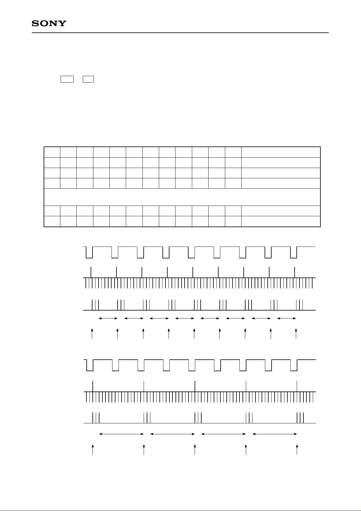
The SG stopped VD period, that is to say the exposure time, can be adjusted from 0 to 4095V in 1V units
by the D11 to D0 setting. Setting all 0 results in the high-speed shutter corresponding to the shutter SUB
setting.
∗
During the SG stopped VD period, data other than 5. TRIG data and 6. Other data are not reflected.
∗
During the SG stopped VD period, only the SG pulse is stopped, and the corresponding V pulse is not
stopped.
∗
During the SG stopped VD period, PBLK, XCPOB and XCPDM are active, and WEN is inactive.
The SG stopped VD period (V) for each serial setting value and the shutter V setting outline diagrams (for
SG stopped VD periods 0V and 1V) are shown below.
D11 SG stopped VD period (V)
D10
D9
D8
D7
D6
D5
D4
D3
D2
D1
D0
CXD3607R
0
0
0
0
0
0
0
0
0
0
0
0
0
0
0
0
0
0
0
0
0
:
1
1
1
1
1
1
1
1
1
1
1
1
1
1
Shutter V setting: 0V = high-speed shutter
VD
V2A
SUB
Exposure time
Serial data
reflected
0
0
0
0
0
0
0
0
0
1
0
0
0
1
0
0
1
2
:
1
1
1
1
0
1
1
1
1
1
4094
4095
Shutter V setting: 1V
VD
V2A
SUB
Exposure time
Serial data
reflected
– 17 –
Page 18

(2) Shutter SUB setting (valid in DRAFT, FINE and TRIGOUT modes)
The charge drain period by the SUB pulse can be adjusted from 1 to 4095H in 1H units by the D11 to D0
setting. The number of SUB pulses for each serial setting value is shown below.
∗
Setting values in excess of the maximum number of pulses per VD period (example: 1068 pulses for
VD = 1068H) are fixed to the maximum number of pulses.
∗
When performing long-time exposure with the shutter V setting, setting values in excess of the maximum
number of pulses per VD period are fixed to the maximum number of pulses.
∗
Setting all 1 results in all SUB output (ALL), for any VD period.
D11 Number of SUB pulses
D10
D9
D8
D7
D6
D5
D4
D3
D2
D1
D0
CXD3607R
0
0
0
0
0
0
0
0
1
1
1
1
1
1
Shutter SUB setting
0
0
0
0
0
0
0
0
0
0
0
0
0
0
0
0
0
0
0
1
0
0
0
0
0
0
0
0
1
0
0
0
0
0
0
0
0
0
1
1
:
1
1
1
1
1
1
1
1
0
1
1
1
1
1
1
1
1
1
1
0
1
1
1
1
1
1
1
1
1
1
1H 2H 3H 4H 4094H 4095H 4096H to
HD
V2A
0
1
2
3
:
4093
4094
4095
(All)
1
1
2
3
:
4093
4094
All
– 18 –
Page 19

5. TRIG data
(1) SG stop setting (valid only during TRIG drive)
SG pulse (ternary value output of the V2A and V2B pulses) stopped/not stopped during TRIG drive can be
selected by the D0 setting.
∗
When SG stopped is selected, the corresponding V pulse is not stopped.
D0 Description of operation
0
SG not stopped (TRIG drive)
1
SG stopped (TRIG drive)
(2) SUB stop setting (valid only during TRIG drive)
SUB pulse stopped/not stopped during TRIG drive can be selected by the D1 setting.
D1 Description of operation
0
SUB not stopped (TRIG drive)
1
SUB stopped (TRIG drive)
CXD3607R
(3) High-speed sweep setting (valid only during TRIG drive)
High-speed sweep on/off during TRIG drive can be selected by the D2 setting.
(For details, see Chart-4 to Chart-7.)
D2 Description of operation
0
High-speed sweep on (TRIG drive)
1
High-speed sweep off (TRIG drive)
∗
The number of V transfers (stages) for high-speed sweep differs according to the drive mode during
TRIG pulse input.
(For details, see Chart-12 and Chart-13.)
DRAFT mode: 20 (stages/H) × 53 (H) = 1060 (stages)
FINE/TRIGOUT mode: 5 (stages/H) × 210 (H) = 1050 (stages)
(4) Clamp pulse stop setting (valid only during TRIG drive)
XCPDM, XCPOB and PBLK stopped/not stopped from SG pulse generation until 7H after the falling edge
of the next valid VD during TRIG drive can be selected by the D3 setting.
(For details, see Chart-4 to Chart-7.)
D3 Description of operation
0
Clamp pulses not stopped (TRIG drive)
1
Clamp pulses stopped (TRIG drive)
– 19 –
Page 20

(5) SG generation position setting (valid only during TRIG drive)
The SG pulse (ternar y value output of the V2A and V2B pulses) generation position dur ing TRIG drive can
be selected from 2 to 2048H counting from the next HD after the f alling edge of the TRIG pulse by the D10
to D0 setting. The SG generation position (H) for each serial setting value is shown below.
(For details, see Chart-4 to Chart-7.)
CXD3607R
D10
D9
D8
D7
D6
D5 D4
0
0
0
0
0
0
0
0
0
0
0
0
0
0
0
0
0
0
0
0
0
0
0
0
D3
D2
D1
D0
0
0
0
0
0
0
0
0
0
0
0
1
0
0
0
1
:
1
1
1
1
1
1
1
1
1
1
1
1
1
1
1
∗
When high-speed sweep is on, a SG generation prohibited area exists. When this area is designated, the SG
1
1
1
1
1
1
1
1
1
1
0
1
1
1
1
SG generation position (H)
0
1
0
1
1
0
1
2046
2047
2048
2
2
3
4
:
pulse is generated at the position indicated below. When the drive mode during TRIG pulse input is:
DRAFT mode: When the prohibited area 2 to 57H is designated, the SG pulse is generated at 58H.
FINE/TRIGOUT mode: When the prohibited area 2 to 214H is designated, the SG pulse is
generated at 215H.
∗
VD input is not accepted until 2H after the SG generation position (H), and is accepted from 3H onward.
(Example: When the SG generation position is 58H, VD input is not accepted from 1 to 59H, and is
accepted from 60H onward.)
(6) SUB setting (valid only during TRIG drive)
The number of SUB pulses during TRIG drive can be selected by the D7 to D0 setting. The number of
SUB pulses for each serial setting value is shown below.
D7
D6
D5
D4
D3
D2
D1
0
0
0
0
0
0
0
0
0
0
0
0
0
0
0
0
0
0
0
0
1
0
0
0
0
0
0
1
:
1
1
0
1
0
1
0
1
1
0
1
0
1
1
1
1
0
1
0
1
1
∗
When high-speed sweep is off, the number of SUB pulses is two regardless of the drive mode during
D0
0
1
0
1
1
0
1
Number of SUB pulses
1
1
2
3
:
213
214
215
TRIG pulse input and the SUB setting value.
∗
When high-speed sweep is on, the maximum number of SUB pulses is as follows according to the drive
mode during TRIG pulse input. Setting values in excess of the maximum number of pulses are fixed to
the maximum number of pulses. (For details, see Chart-4 to Char t-7.)
DRAFT mode: Max. 58 pulses
FINE/TRIGOUT mode: Max. 215 pulses
– 20 –
Page 21

6. Other data
(1) Standby setting
Standby operation can be selected by the D0 setting. The Pin Status Table during standby operation is
shown below.
∗
The standby setting bit is loaded at the rising edge of the second SCK clock after the rising edge of
SEN, and control is applied immediately.
∗
Serial data is loaded as normal during standby operation.
D0 Description of operation
01Normal operation
Standby operation
Pin Status Table (Standby setting bit = 1)
CXD3607R
Pin No.
1
2
3
4
5
6
7
8
9
10
11
12
13
14
15
16
Symbol
VSS4
RST
SYNSL
NC
NC
NC
VDD4
TEST1
TEST2
RG
VSS1
H1
H2
VDD1
VDD2
XSHD
I/O status
—
ACT
ACT
—
—
—
—
—
—
L
—
L
L
—
—
L
Pin No. Symbol I/O status
25
26
27
28
29
30
31
32
33
34
35
36
37
38
39
40
CKI
OSCO
OSCI
VDD3
SSI
SCK
SEN
VD
HD
TRIG
WEN
VSS3
VM
V1
V4
V2A
ACT
ACT
ACT
—
ACT
ACT
ACT
DIS
DIS
DIS
L
—
—
VM
VM
VH
17
18
19
20
21
22
23
24
XSHP
XCPDM
XCPOB
PBLK
ADCLK
MCKO
CKO
VSS2
L
L
L
L
L
ACT
ACT
—
41
42
43
44
45
46
47
48
VH
V2B
NC
NC
VL
NC
V3
SUB
—
VH
—
—
—
—
VM
VH
Note) ACT means that the circuit is operating, and DIS means that loading is stopped.
L indicates a low output level, and H a high output level in the controlled state.
VM and VL indicate the voltage levels applied to VM (Pin 37) and VL (Pin 45), respectively.
– 21 –
Page 22

CXD3607R
Detailed Description of Output Pins
The CXD3607R generates special pulses that are used by signal processing circuits, etc. These details are
described below.
• WEN (Pin 30)
The CXD3607R outputs a WEN signal that indicates the effective line period output from the CCD image
sensor. The WEN signal is high during the vertical effective line period. For details, see the vertical timing
charts for each drive mode.
∗
When SG stopped is selected by the SG stop setting, WEN is inactive during the SG stopped VD per iod.
∗
When performing long-time exposure with the shutter V setting, WEN is inactive during the SG stopped VD
period.
Special Drive Sequence (Random trigger shutter drive)
Cameras using the CXD3607R can perform random trigger shutter drive which allows image capturing at an
optional timing. The TRIG pulse is loaded from the TRIG pin at the rising edge of MCKO, and reflected from the
falling edge of the next HD.
The random trigger shutter drive sequence in DRAFT mode is shown below.
(1)
TRIG
VD
HD
Mode
V2A
SUB
CCDOUT
XCPOB, XCPDM
DRAFT DRAFT (TRIG function enabled)
(4) SG generation position setting
(2) High-speed sweep setting
(3) SUB setting
Exposure A Exposure C
Exposure A
(part-way)
Not accepted
Not accepted
TRIGOUT DRAFT
(6) SG and V pulse stopped
Main exposure
None
(5) Clamp pulse stop setting
ExposureExposure B
Exposure CMain exposure
– 22 –
Page 23

CXD3607R
(1) If the drive mode data “TRIG function setting” is 1: Enabled at the falling edge of the TRIG pulse, operation
switches to TRIG drive.
∗
Operation cannot be guaranteed for a TRIG pulse low-active period of 2H or less.
∗
The TRIG pulse is valid when input with the falling edge synchronized to the falling edge of VD.
∗
The TRIG pulse is not accepted after switching to TRIG drive.
∗
The VD pulse is not accepted for until 2H after SG generation after switching to TRIG drive. Serial data is
also not reflected by the falling edge of VD during this per iod. (Example: When SG is generated at 58H,
VD is not accepted from 1 to 59H)
(2) Operation switches to TRIG drive mode and high-speed sweep for ver tical register block charge drain
starts from the falling edge of the next HD after the falling edge of the input TRIG pulse. The number of
high-speed sweep stages differs according to the drive mode at the falling edge of the TRIG pulse as
follows. DRAFT: 20 (stages/H) × 53 (H) = 1060 (stages), FINE/TRIGOUT: 5 (stages/H) × 210 (H) = 1050
(stages). High-speed sweep off can also be selected by the TRIG data “High-speed sweep setting”.
(3) The charge drain period using the SUB pulse can be selected by the TRIG data “SUB setting”.
When high-speed sweep is on, the maximum number of SUB pulses is as follows according to the drive
mode at the falling edge of the TRIG pulse. DRAFT: max. 58 pulses, FINE/TRIGOUT: max. 215 pulses.
When high-speed sweep is off, the number of SUB pulses is two regardless of the drive mode at the falling
edge of the TRIG pulse and the SUB setting value.
(4) The SG pulse generation position can be selected by the TRIG data “SG generation position setting”. After
SG pulse output, V transfer is not performed and standby mode is established until the next VD input.
(5) The clamp pulses can also be stopped after SG pulse generation by the TRIG data “Clamp pulse stop
setting”.
(6) Be sure to drive in TRIGOUT mode during the next VD period after TRIG drive. (Operation in other modes
can be not guaranteed.)
∗
TRIG drive ends at the first VD input 3H onward after SG pulse generation. Even when operation shifted
to TRIG drive during long-time exposure using the “Shutter V setting”, note that serial data is always
reflected at the first VD input 3H onward after SG pulse generation.
Specifications for Each Drive Mode and A Table Corresponding Timing Char ts
Drive mode
DRAFT
FINE
TRIGOUT
DRAFT → TRIG
(high-speed
sweep on)
Frame
rate (s)
1/60
1/15
1/15
—
Total
number
of HD (H)
267
1068
1068
—
High-speed
sweep H
period (H)
0
0
0
53
(fixed)
Number of highspeed sweep
stages (stage)
0
0
0
1060
(fixed)
Vertical
timing
chart
Chart-1
Chart-2
Chart-3
Chart-4
Readout
block H
chart
Chart-8
Chart-10
—
Chart-10
DRAFT → TRIG
(high-speed
—
—
0
0
Chart-5
Chart-10
sweep off)
FINE/TRIGOUT
→ TRIG
(high-speed
—
—
210
(fixed)
1050
(fixed)
Chart-6
Chart-10
sweep on)
FINE/TRIGOUT
→ TRIG
(high-speed
—
—
0
0
Chart-7
Chart-10
sweep off)
Normal
transfer block
H chart
Chart-9
Chart-11
Chart-11
—
—
—
—
High-speed
sweep block
H chart
—
—
—
Chart-12
—
Chart-13
—
– 23 –
Page 24

CXD3607R
MODE
DRAFT mode
1/60s
VD
HD
19
18
17
16
15
14
13
12
11
10
9
8
7
6
5
4
3
2
1
267
266
265
264
263
262
261
260
259
258
257
256
255
254
253
252
251
250
249
248
27
26
25
24
23
22
21
20
19
18
17
16
15
14
13
12
11
10
9
8
7
6
5
4
3
2
1
Readout block (Chart-8) Normal transfer block (Chart-9)
267
266
265
264
263
262
261
260
V1
V2A
V2B
V3
V4
SUB
XCPOB
XCPDM
260H
PBLK
WEN
57
49
41
33
25
17
9
1
1
1
993
985
977
89
81
73
65
57
49
41
33
25
17
9
1
1
1
1033
1025
1017
1009
1001
1033
1025
OUT
60
52
44
36
28
20
12
4
4
996
988
980
92
84
76
68
60
52
44
36
28
20
12
4
4
1036
1028
1020
1012
1004
1036
1028
19
18
17
16
15
14
13
12
11
10
9
8
7
6
5
4
3
2
1
267
266
265
264
263
262
261
260
259
258
257
256
255
254
253
252
251
250
249
248
27
26
25
24
23
22
21
20
19
18
17
16
15
14
13
12
11
10
9
8
7
6
5
4
3
2
1
267
266
265
264
263
262
261
260
DRAFT DRAFT DRAFT
TRIG function disabled TRIG function disabled
TRIG function disabled
The number of SUB pulses is determined by the serial interface data.
∗
Drive mode setting
TRIG function setting
Chart-1 Vertical Timing Chart
– 24 –
Page 25

CXD3607R
MODE
FINE mode
1/15s
VD
HD
17
16
15
14
13
12
11
10
9
8
7
6
5
4
3
2
1
1068
1067
1066
1065
1064
1063
1062
1061
1060
1059
1058
1057
1056
1055
1054
1053
1052
1051
1050
1049
1048
1047
1046
1045
27
26
25
24
23
22
21
20
19
18
17
16
15
14
13
12
11
10
9
8
7
6
5
4
3
2
1
Readout block (Chart-10) Normal transfer block (Chart-11)
1068
1067
1066
1065
1064
1063
1062
1061
V1
V2A
V2B
V3
V4
SUB
XCPOB
XCPDM
PBLK
1040H
WEN
5
4
3
2
1
8
7
6
5
4
3
2
1
2
1
1040
1039
1038
1037
1036
1035
1034
1033
15
14
13
12
11
10
9
8
7
6
5
4
3
2
1
8
7
6
5
4
3
2
1
OUT
17
16
15
14
13
12
11
10
9
8
7
6
5
4
3
2
1
1068
1067
1066
1065
1064
1063
1062
1061
1060
1059
1058
1057
1056
1055
1054
1053
1052
1051
1050
1049
1048
1047
1046
1045
27
26
25
24
23
22
21
20
19
18
17
16
15
14
13
12
11
10
9
8
7
6
5
4
3
2
1
1068
1067
1066
1065
1064
1063
1062
1061
FINE FINE FINE
TRIG function disabled TRIG function disabled
TRIG function disabled
The number of SUB pulses is determined by the serial interface data.
∗
Drive mode setting
Chart-2 Vertical Timing Chart
– 25 –
TRIG function setting
Page 26

CXD3607R
MODE
TRIGOUT mode
1/15s
VD
HD
17
16
15
14
13
12
11
10
9
8
7
6
5
4
3
2
1
1068
1067
1066
1065
1064
1063
1062
1061
1060
1059
1058
1057
1056
1055
1054
1053
1052
1051
1050
1049
1048
1047
1046
1045
27
26
25
24
23
22
21
20
19
18
17
16
15
14
13
12
11
10
Normal transfer block (Chart-11)
9
8
7
6
5
4
3
2
1
1068
1067
1066
1065
1064
1063
1062
1061
V1
V2A
V2B
V3
V4
SUB
XCPOB
XCPDM
PBLK
1040H
WEN
5
4
3
2
1
8
7
6
5
4
3
2
1
2
1
1040
1039
1038
1037
1036
1035
1034
1033
15
14
13
12
11
10
9
8
7
6
5
4
3
2
1
8
7
6
5
4
3
2
1
OUT
17
16
15
14
13
12
11
10
9
8
7
6
5
4
3
2
1
1068
1067
1066
1065
1064
1063
1062
1061
1060
1059
1058
1057
1056
1055
1054
1053
1052
1051
1050
1049
1048
1047
1046
1045
27
26
25
24
23
22
21
20
19
18
17
16
15
14
13
12
11
10
9
8
7
6
5
4
3
2
1
1068
1067
1066
1065
1064
1063
1062
1061
TRIG function disabled TRIG function disabled
TRIGOUT TRIGOUT TRIGOUT
TRIG function disabled
The number of SUB pulses is determined by the serial interface data.
∗
Drive mode setting
Chart-3 Vertical Timing Chart
– 26 –
TRIG function setting
Page 27

Chart-4 Vertical Timing Chart
MODE
DRAFT mode → TRIG drive
(High-speed sweep on, SG generation position: 58H, SUB setting: 58 pulses)
TRIG
∗
The VD fall is not accepted until 2H after SG generation.
(Example: When the SG generation position is 58H, VD input is not accepted from 1 to 59H, and is accepted from 60H onward.)
VD
HD
V1
260
261
262
263
264
265
266
12354
267
678
9
10111213141516
High-speed sweep block (Chart-12)
Fixed to 53H (20 stages × 53H = 1060 stages)
12345
17
SG prohibited area (1 to 57H)
687
9
505152
10
Selectable in the range of 58 to 2048H by the
SG generation position setting. (Example: 58H)
545556
53
Readout block (Chart-10)
57
585960
61
241
240
242
243
245
244
246
247
123456789
248
249
250
10111213151416
17
V2A
V2B
V3
– 27 –
V4
SUB
XCPOB
Selectable from 1 to 58 pulses by the SUB setting. (Example: 58 pulses)
XCPDM
PBLK
These pulses can be stopped by
WEN
the clamp pulse stop setting.
OUT
Drive mode setting
TRIG fuction setting
1025
260
1028
261
1033
262
1036
263
1
264
265
266
12354
267
14149
1217202528333641444952
678
9
10111213141516
12345
17
687
9
10
505152
53
545556
57
585960
61
240
241
243
242
244
245
246
247
123456789
248
249
250
1234567812345
DRAFT DRAFT TRIGOUT
TRIG function disabled
∗
The number of SUB pulses is determined by the serial interface data.
TRIG function enabled TRIG function disabled
10111213151416
17
CXD3607R
Page 28
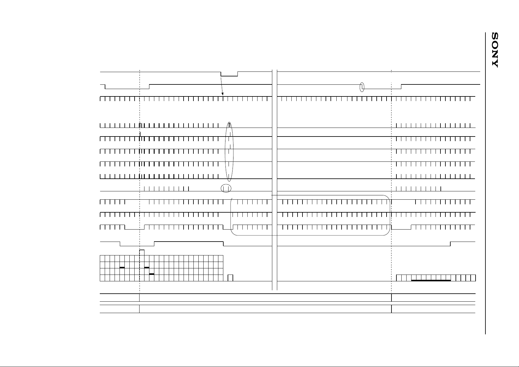
Chart-5 Vertical Timing Chart
MODE
DRAFT mode → TRIG drive
(High-speed sweep off, SG generation position: 2H, SUB setting: fixed to 2 pulses)
TRIG
∗
The VD fall is not accepted until 2H after SG generation.
(Example: When the SG generation position is 2H, VD input is not accepted from 1 to 3H, and is accepted from 4H onward.)
VD
HD
260
261
262
263
264
123546789
265
266
267
10111213141516
Readout block (Chart-10)
Selectable in the range of 2 to 2048H by the
SG generation position setting. (Example: 2H)
12345
17
687
9
10
228
229
230
231
232
233
234
235
236
237
238
239
240
241
242
243
244
245
246
247
123456789
248
249
250
10111213141615
17
V1
V2A
V2B
V3
– 28 –
V4
SUB
Fixed to two pulses regardless of the SUB setting.
XCPOB
XCPDM
PBLK
WEN
These pulses can be stopped by the clamp pulse stop setting.
OUT
Drive mode setting
TRIG fuction setting
1025
260
1028
261
1033
262
1036
263
1
264
265
14149
123546789
266
267
1217202528333641444952
10111213141516
12345
17
687
9
10
228
229
231
230
232
233
234
235
236
237
238
239
240
241
242
243
244
245
246
247
123456789
248
249
250
1234567812345
DRAFT DRAFT TRIGOUT
TRIG function disabled
∗
The number of SUB pulses is determined by the serial interface data.
TRIG function enabled
TRIG function disabled
10111312141516
17
CXD3607R
Page 29

Chart-6 Vertical Timing Chart MODE
FINE/TRIGOUT mode → TRIG drive
(High-speed sweep on, SG generation position: 215H, SUB setting: 215 pulses)
TRIG
VD
∗
The VD fall is not accepted until 2H after SG generation.
(Example: When the SG generation position is 215H, VD input is not accepted from 1 to 216H, and is accepted from 217H onward.)
– 29 –
Drive mode setting
HD
V1
V2A
V2B
V3
V4
SUB
XCPOB
XCPDM
PBLK
WEN
OUT
1061
1061
1062
1062
1063
1063
1064
1064
1065
1065
123546789
1066
1067
1068
123546789
1066
1067
1068
12345
10111213141516
High-speed sweep block (Chart-13)
Fixed to 210H (5 stages × 210H = 1050 stages)
Selectable from 1 to 215 pulses by the SUB setting. (Example: 215 pulses)
12345
678
10111213141516
12345
17
SG prohibited area (1 to 214H)
12345
17
687
687
9
10
207
Selectable in the range of 215 to 2048H by the
SG generation position setting. (Example: 215H)
9
10
207
211
212
213
211
212
213
214
214
215
215
208
209
210
Readout block (Chart-10)
208
209
210
216
216
217
218
1041
1042
1044
1043
1045
These pulses can be stopped by
the clamp pulse stop setting.
217
218
1041
1042
1044
1043
1045
1046
1046
1047
1047
1048
1048
123456789
1049
1050
1051
123456789
1049
1050
1051
1
FINE FINE TRIGOUT
10111213151416
23456781234
10111312141516
17
5
17
TRIG fuction setting
TRIG function disabled
∗
The number of SUB pulses is determined by the serial interface data.
TRIG function enabled TRIG function disabled
CXD3607R
Page 30

Chart-7 Vertical Timing Chart
MODE
FINE/TRIGOUT mode → TRIG drive
(High-speed sweep off, SG generation position: 2H, SUB setting: fixed to 2 pulses)
TRIG
∗
The VD fall is not accepted until 2H after SG generation.
(Example: When the SG generation position is 2H, VD input is not accepted from 1 to 3H, and is accepted from 4H onward.)
VD
HD
1061
1062
1063
1064
1065
1066
1067
12354
1068
678
9
10111213141516
Selectable in the range of 2 to 2048H by the
SG generation position setting. (Example: 2H)
12345
17
Readout block (Chart-10)
687
9
10
1029
1030
1031
1032
1033
1034
1035
1036
1037
1038
1039
1040
1041
1042
1043
1044
1045
1046
1047
1048
123456789
1049
1050
1051
10111213141615
17
V1
V2A
V2B
V3
– 30 –
V4
SUB
Fixed to two pulses regardless of the SUB setting.
XCPOB
XCPDM
PBLK
WEN
These pulses can be stopped by the clamp pulse stop setting.
OUT
Drive mode setting
TRIG fuction setting
1061
1062
1063
1064
1065
1066
1067
12354
1068
12345
678
9
12345
678
10111213141516
12345
17
687
9
10
1029
1030
1032
1031
1033
1034
1035
1036
1037
1038
1039
1040
1041
1042
1043
1044
1045
1046
1047
1048
123456789
1049
1050
1051
1234567812345
FINE FINE TRIGOUT
TRIG function disabled
∗
The number of SUB pulses is determined by the serial interface data.
TRIG function enabled
TRIG function disabled
10111312141516
17
CXD3607R
Page 31

Chart-8 Horizontal Timing Char t
MODE
DRAFT mode readout block
(1790) (1790)
0
50
100 150 200 250 300 350 400 800 850 900 950 1000 1050 0 50
1H
HD
180 17900
MCKO
OUT
443
380
DM (20)
400 402
OB (40)OB (40)
443
H1
43
H2
43
V1
66
118 234 286 318 1011 1063 66
150 202
V2A
– 31 –
55 87 139 171 223 255 307 1032 55 87
339
380
380
804
801
43
43
906
1000
V2B
55 87 139 171 223 255 307
339 1032 55 87
1000
V3
76
108 160 192 244 276 328 360 1021 76
1053
V4
45 97 129 181
213 265
297
349
990 1042 45 97
SUB
150
276
PBLK
XCPOB
XCPDM
WEN
398
382
∗
The HD of this chart indicates the actual CXD3607R load timing.
∗
The numbers at the output pulse transition points indicate the count at the MCKO rise from the fall of HD.
CXD3607R
Page 32

Chart-9 Horizontal Timing Char t
MODE
DRAFT mode normal transfer block
– 32 –
HD
MCKO
OUT
H1
H2
V1
V2A
V2B
V3
V4
SUB
PBLK
XCPOB
XCPDM
WEN
(1790) (1790)
0
50
443
43
43
66
55 87 139 171 223 255 55 87
55 87 139 171 223 255
45
44
12 42
100 150 200 250 300 350 400 450 500 550 600 650 700 0 50
2H to
180 17900
DM (20)
380
400 402
380
380
150 202
118 234 286 318 370
307
339
307
339 55 87
108 160 192 244 276 328 360 76
76
97 129 181
150
213 265 45
276
211
349297
400
398
382
OB (40)OB (40)
443
43
43
66
97
44
12 42
CXD3607R
∗
The HD of this chart indicates the actual CXD3607R load timing.
∗
The numbers at the output pulse transition points indicate the count at the MCKO rise from the fall of HD.
Page 33
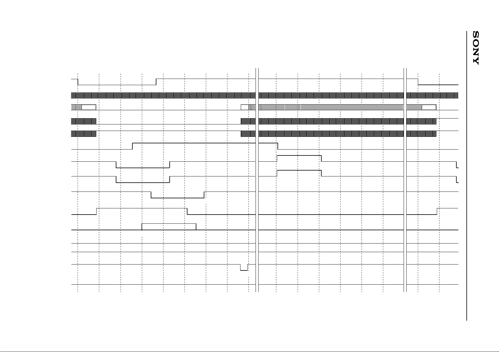
Chart-10 Horizontal Timing Chart
MODE
FINE mode readout block
(1790) (1790)
0
50
100 150 200 250 300 350 400 800 850 900 950 1000 1050 0 50
1H
HD
180 17900
MCKO
OUT
443
380
DM (20)
400 402
OB (40)OB (40)
443
H1
43
H2
43
V1
V2A
– 33 –
129 804
87 213
V2B
87 213
380
380
43
43
801 906
87
801 906
87
V3
171
297
V4
45
255 45
SUB
150
276
PBLK
XCPOB
XCPDM
WEN
382
398
∗
The HD of this chart indicates the actual CXD3607R load timing.
∗
The numbers at the output pulse transition points indicate the count at the MCKO rise from the fall of HD.
CXD3607R
Page 34

Chart-11 Horizontal Timing Chart
(1790) (1790)
0
HD
MCKO
50
100 150 200 250 300 350 400 450 500 550 600 650 700 0 50
2H to
MODE
FINE/TRIGOUT mode normal transfer block
180 17900
– 34 –
OUT
H1
H2
V1
V2A
V2B
V3
V4
SUB
PBLK
XCPOB
XCPDM
WEN
443
43
43
129 339
87 213 87
87 213 87
171 297
45 255
150
44
12 42 12 42
211
276
380
382
DM (20)
400 402
380
380
400
398
OB (40)OB (40)
443
43
43
45
44
CXD3607R
∗
The HD of this chart indicates the actual CXD3607R load timing.
∗
The numbers at the output pulse transition points indicate the count at the MCKO rise from the fall of HD.
Page 35

Chart-12 Horizontal Timing Chart
MODE
DRAFT mode → TRIG drive high-speed sweep block
– 35 –
HD
MCKO
OUT
H1
H2
V1
V2A
V2B
V3
V4
SUB
PBLK
XCPOB
XCPDM
(1790) (1790)
0
0
443
12 42
After the fall of TRIG
50
43
43
45
44
100 150 200 250 300 350 400 450 500 1600 1650 1700 1750 0 50
1H to
180
DM (20)
380
400 402
380
#1 #2 #3 #4 #5 #19 #20 #1
66
55 87 139 171 223 255 307 55 87
55 87 139 171 223 255 307
76
97 129 181
150 202
118 234 286 318 370 402 486
339 423 475
339 55 87
108 160 192 244 276 328 360 412 444 496 76
213 265 297 349 381 433 465 45 97
150
276
380
391
391
454
423 475
1630 1662 1714
1599
1567 1683
1599
1567
1588
1557 1609 1641 1693
1651
1651
1620 1672
1683
1704
1790
OB (40)OB (40)
443
43
43
661578
WEN
211
∗
The HD of this chart indicates the actual CXD3607R load timing.
∗
The numbers at the output pulse transition points indicate the count at the MCKO rise from the fall of HD.
CXD3607R
Page 36

Chart-13 Horizontal Timing Chart
MODE
FINE/TRIGOUT mode → TRIG drive high-speed sweep block
– 36 –
HD
MCKO
OUT
H1
H2
V1
V2A
V2B
V3
V4
SUB
PBLK
XCPOB
XCPDM
(1790) (1790)
0
443
12 42
After the fall of TRIG
50
43
43
45 255 381 45
44
100 150 200 250 300 350 400 450 500 550 1650 1700 1750 0 50
1H to
180 17900
DM (20)
380
400 402
380
#1 #2 #5 #1
129 339 465 1683
87 213 423 549 87
87 213 87
171 297
150
276
380
423 549
507 1641
OB (40)OB (40)
443
43
43
WEN
211
∗
The HD of this chart indicates the actual CXD3607R load timing.
∗
The numbers at the output pulse transition points indicate the count at the MCKO rise from the fall of HD.
CXD3607R
Page 37

Chart-14 High-Speed Phase Timing Char t MODE
DRAFT/FINE/TRIGOUT mode
HD
HD'
CKI
CKO
123456740414243444546
MCKO
– 37 –
H1
H2
377 378 379 380 381 382
RG
XSHP
(Logical phase 90˚)
XSHD
(Logical phase 90˚)
ADCLK
(Logical phase 0˚)
∗
HD’ indicates the HD which is the actual CXD3607R load timing. (when MCKO sync is selected)
∗
The phase relationship of each pulse shows the logical position relationship. For the actual output waveform, a delay is added to each pulse.
∗
The logical phases of XSHP, XSHD and ADCLK can be specified by the serial interface data.
CXD3607R
Page 38

Application Circuit Block Diagram
CXD3607R
CCD
ICX285
CCD OUT
H1
H2
RG
V1
V2A
V2B
V3
V4
SUB
12
13
10
38
40
42
47
39
48
V-Dr
25 26
CKI
CDS/ADC Block
XSHP
XSHD
16
17 18 19
CXD3607R
27
OSCI
OSCO
XCPOB
XCPDM
TG
8 9
TEST2
TEST1
PBLK
20 21
29
ADCLK
30
SSI
SCK
Digital OUT
22
23
35
32
33
34
2
3
31
SEN
MCKO
CKO
WEN
VD
HD
TRIG
RST
SYNSL
Signal
Processor
Block
Controller
This block diagram shows the connection relationship with each block, and is not an actual circuit diagram.
See the CCD image sensor data sheet for a concrete example of circuit connection with a CCD image sensor.
Application circuits shown are typical examples illustrating the operation of the devices. Sony cannot assume responsibility for
any problems arising out of the use of these circuits or for any infringement of third party patent and other right due to same.
Notes for Power-on
Of the four –7.0V, +15.0V, +3.3V, +5.0V power supplies, be sure to start up the –7.0V and +15.0V power
supplies in the following order to prevent the SUB pin of the CCD image sensor from going to negative
potential.
15V
t1
20%
20%
0V
t2
t2 ≥ t1
–7.0V
– 38 –
Page 39

Package Outline Unit: mm
9.0 ± 0.2
∗ 7.0 ± 0.1
CXD3607R
48PIN LQFP (PLASTIC)
37
48
0.5
36
1
0˚ to 10˚
+ 0.08
0.18 – 0.03
25
12
0.1 ± 0.1
0.5 ± 0.2
24
13
(0.22)
0.13
S
(8.0)
A
B
0.5 ± 0.2
+ 0.05
0.127 – 0.02
+ 0.2
M
1.5 – 0.1
0.1
S
0.18 ± 0.03
0.127 ± 0.04
DETAIL B: PALLADIUM
SONY CODE
EIAJ CODE
JEDEC CODE
DETAIL A
LQFP-48P-L01
P-LQFP48-7x7-0.5
NOTE: Dimension “∗” does not include mold protrusion.
PACKAGE STRUCTURE
PACKAGE MATERIAL
LEAD TREA TMENT
LEAD MATERIAL
PACKAGE MASS
EPOXY RESIN
PALLADIUM PLATING
COPPER ALLOY
0.2g
– 39 –
Sony Corporation
 Loading...