

Page 1

CXD3400N
6-channel CCD Vertical Clock Driver
Description
The CXD3400N is a vertical clock driver for CCD
image sensor. This IC is composed of 6 channels
which supports high frame rate readout mode.
Features
• Composition
Vertical transfer output 3 levels driver × 4
2 levels driver × 2
Electronic shutter output 2 levels driver × 1
• Suitable drive capability for high-pixel CCD
(40% improved compared to current device)
• Small package (20-pin SSOP)
• 2.7 to 5.5V supported input interface
Applications
Digital still camera
Structure
CMOS
Absolute Maximum Ratings
• Supply voltage VDD GND – 0.3 to +7.0 V
• Supply voltage VL GND to –10 V
• Supply voltage VH VL + 26 V
• Input voltage VIN GND – 0.3V to VDD + 0.3 V
• Operating temperature Topr –20 to +75 °C
• Storage temperature Tstg –55 to +150 °C
Recommended Operating Conditions
• Supply voltage VDD 2.7 to 5.5 V
• Supply voltage VL –5.0 to –9.0 V
• Supply voltage VH 11.5 to 15.5 V
• Operating temperature Topr –20 to +75 °C
– 1 –
E98Y42A9X
Sony reserves the right to change products and specifications without prior notice. This information does not convey any license by
any implication or otherwise under any patents or other right. Application circuits shown, if any, are typical examples illustrating the
operation of the devices. Sony cannot assume responsibility for any problems arising out of the use of these circuits.
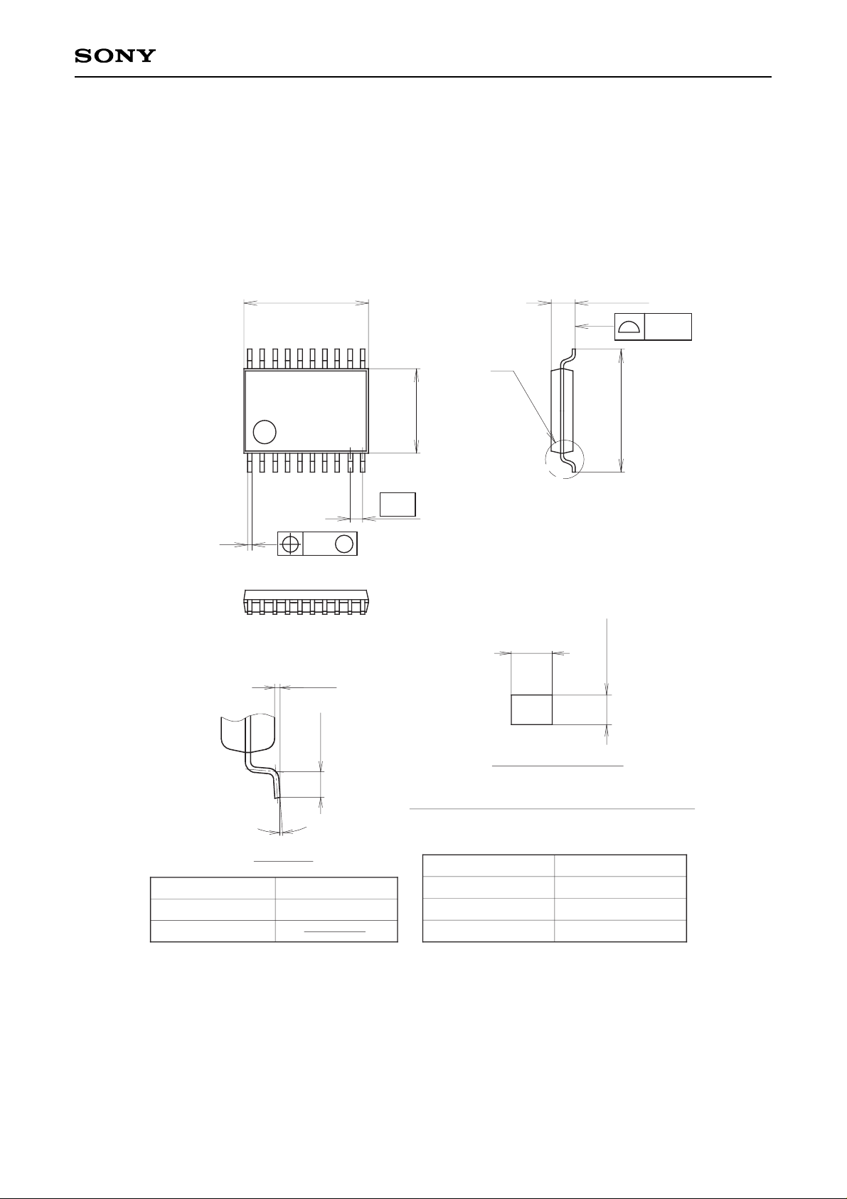
20 pin SSOP (Plastic)
Page 2

– 2 –
CXD3400N
Block Diagram
11
12
13
14
15
16
17
18
19
20
1
2
3
4
5
6
7
8
9
10 GND
V2
V4
V1A
V
H
V1B
V3A
V
L
V3B
SHT
XV2
XV4
XSG1A
XSG1B
XV1
XSG3A
XSG3B
XV3
XSHT
V
DD
Input Buffer
Pin Description
Pin
No.
1
2
3
4
5
6
7
8
9
10
11
12
13
14
15
16
17
18
19
20
VDD
XSHT
XV3
XSG3B
XSG3A
XV1
XSG1B
XSG1A
XV4
XV2
GND
V2
V4
V1A
VH
V1B
V3A
VL
V3B
SHT
Symbol
—
I
I
I
I
I
I
I
I
I
—
O
O
O
—
O
O
—
O
O
I/O
Input power supply (3.3V system)
SHT pulse input
V3A and V3B transfer pulse input
V3B readout pulse input
V3A readout pulse input
V1A and V1B readout pulse input
V1B readout pulse input
V1A readout pulse input
V4 transfer pulse input
V2 transfer pulse input
GND (= VM)
High voltage output (2 levels: VM, VL)
High voltage output (2 levels: VM, VL)
High voltage output (3 levels: VH, VM, VL)
Positive power supply for high voltage output (15V system)
High voltage output (3 levels: VH, VM, VL)
High voltage output (3 levels: VH, VM, VL)
Negative power supply for high voltage output (–7.5V system)
High voltage output (3 levels: VH, VM, VL)
High voltage output (2 levels: VH, VL)
Functions
Page 3

– 3 –
CXD3400N
Truth Table
Input
XV1, 3
L
L
H
H
X
X
X
X
L
H
L
H
X
X
X
X
X
X
X
X
L
H
X
X
X
X
X
X
X
X
L
H
VH
VM
Z
VL
X
X
X
X
X
X
X
X
VM
VL
X
X
X
X
X
X
X
X
VH
VL
XSG1A, 1B, 3A, 3B
XV2, 4 XSHT
V1A, 1B, 3A, 3B
V2, 4 SHT
Output
Z: High impedance X: Don't care
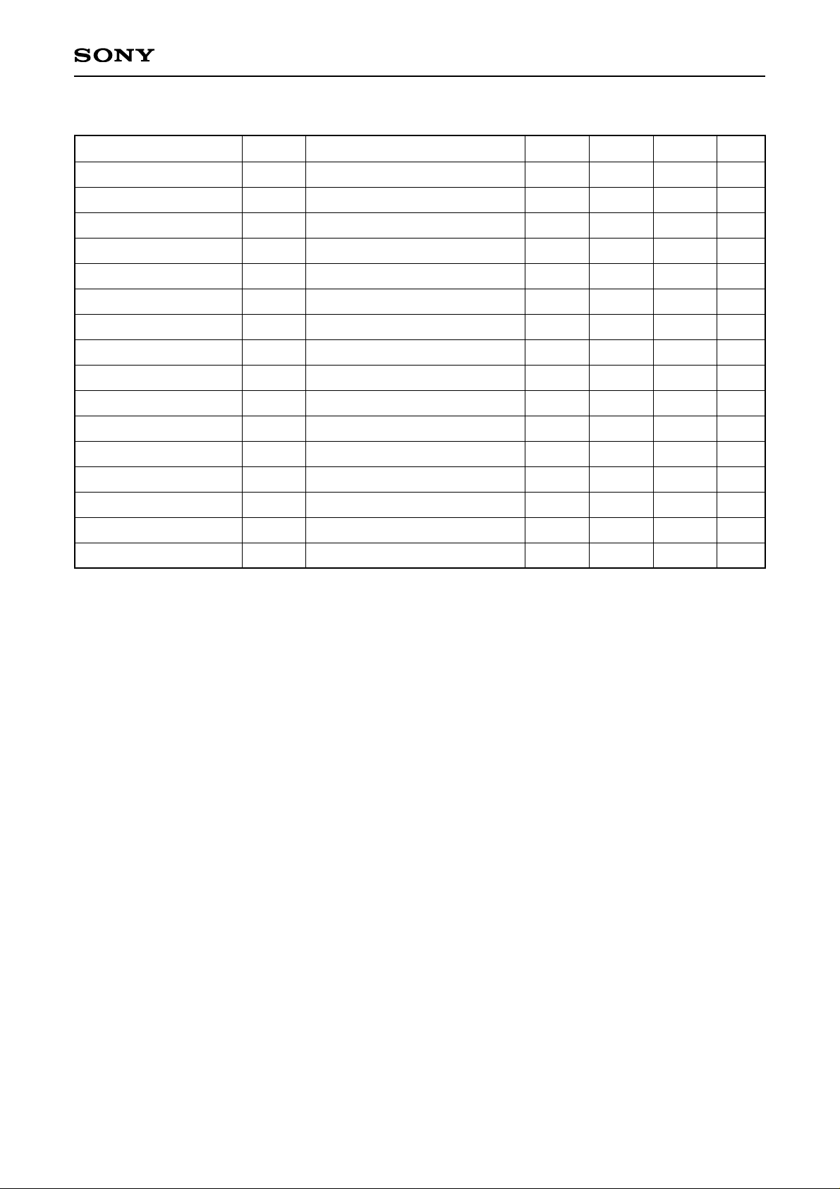
Electrical Characteristics
DC Characteristics (VDD = 3.3V, VH = 15V, VM = GND, VL = –8.5V)
Item
"H" level input voltage
"L" level input voltage
Input current
Operating supply current
Operating supply current
Operating supply current
Output current
Output current
Output current
Output current
Output current
Output current
VIH
VIL
IIN
IH
IDD
IL
IOL
IOM1
IOM2
IOH
IOSL
IOSH
VIN = GND to 5V
∗1
∗1
∗1
V1A, 1B, 3A, 3B, V2, 4 = –8.25V
V1A, 1B, 3A, 3B, V2, 4 = –0.25V
V1A, 1B, 3A, 3B = 0.25V
V1A, 1B, 3A, 3B = 14.75V
SHT = –8.25V
SHT = 14.75V
0.7VDD
—
–10
—
—
–8.5
10
—
5.0
—
5.4
—
—
—
0.0
0.10
0.25
–5.5
—
—
—
—
—
—
—
0.3VDD
10
0.20
0.50
—
—
–5.0
—
–7.2
—
–4.0
V
V
µA
mA
mA
mA
mA
mA
mA
mA
mA
mA
Symbol Conditions Min. Typ. Max. Unit
∗1
See Measurement Circuit. Shutter speed 1/10000
Note) Current direction +: inflow to IC; –: outflow from IC
Page 4
– 4 –
CXD3400N
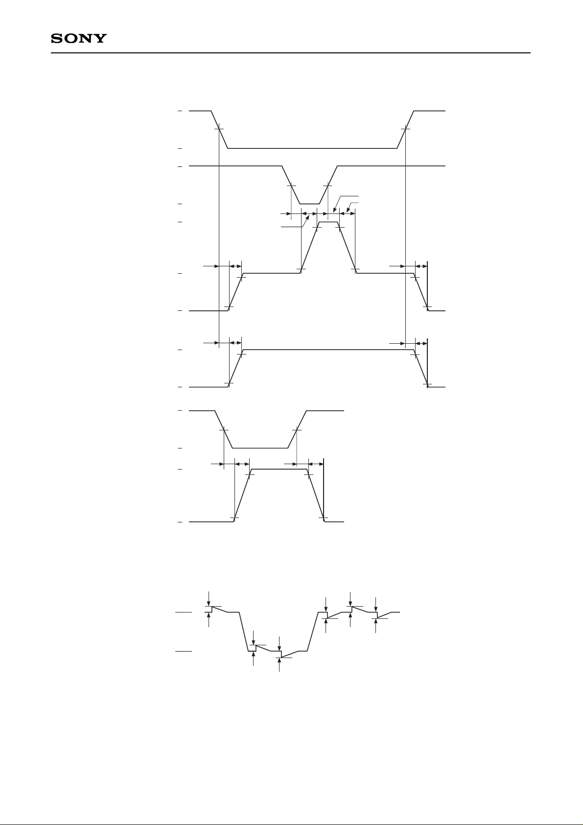
Switching Characteristics (VDD = 3.3V, VH = 15V, VM = GND, VL = –7.5V)
Item
Propagation delay time
Propagation delay time
Propagation delay time
Propagation delay time
Propagation delay time
Propagation delay time
Rise time
Rise time
Rise time
Fall time
Fall time
Fall time
Output noise voltage
Output noise voltage
Output noise voltage
Output noise voltage
TPLM
TPMH
TPLH
TPML
TPHM
TPHL
TTLM
TTMH
TTLH
TTML
TTHM
TTHL
VCLH
VCLL
VCMH
VCML
∗1
∗1
∗1
∗1
∗1
∗1
VL → VM
∗1
VM → VH
∗1
VL → VH
∗1
VM → VL
∗1
VH → VM
∗1
VH → VL
∗1
∗2
∗2
∗2
∗2
50
50
50
10
10
10
200
200
30
200
200
30
—
—
—
—
70
70
70
30
30
30
350
350
60
350
350
60
—
—
—
—
100
100
100
50
50
50
500
500
90
500
500
90
1.0
1.0
1.0
1.0
ns
ns
ns
ns
ns
ns
ns
ns
ns
ns
ns
ns
V
V
V
V
Symbol Conditions Min. Typ. Max. Unit
∗1
See Switching Waveform.
∗2
See Noise on a Waveform.
Note) Each item is evaluated by Measurement Circuit.
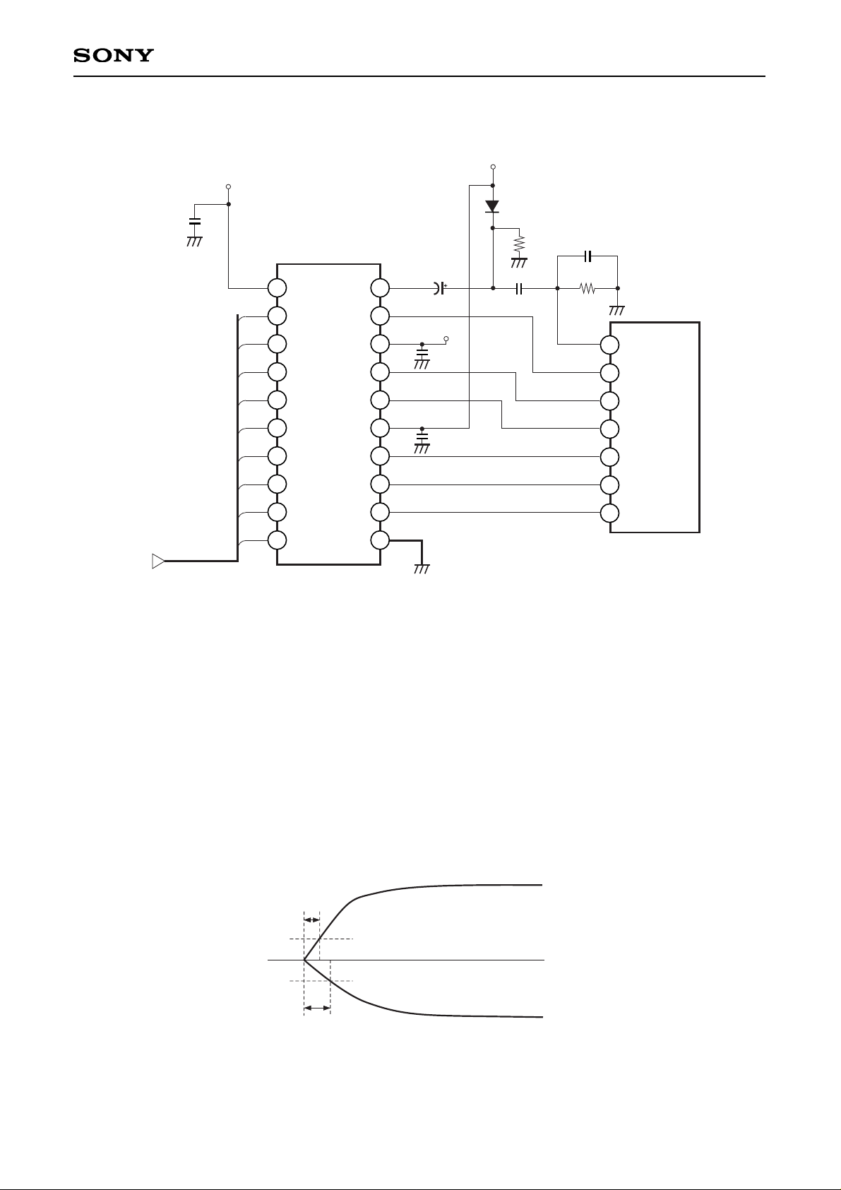
Notes on Operation (See Application Circuit.)
1. Be sure to protect against static electricity because this IC is MOS structure.
2. A bypass capacitor (0.1µF or more) is connected between GND and near each power supply (VH, VDD, VL).
3. In order to protect CCD image sensor, input SHT pin output to SUB pin of CCD image sensor after that has
been clamped at VH.
Page 5
– 5 –
CXD3400N
Switching Waveform
XV1 to 4
XSG1A, 1B, 3A, 3B
V1A, 1B, 3A, 3B
V2, 4
XSHT
SHT
V
DD (3.3V)
VDD (3.3V)
50%
VDD (3.3V)
GND
GND
T
TLM
TTML
TPLM
TPMH
TTMH
TPML
TPHM
TTHM
VH
GND
VH
VM
VL
VL
VL
VM
50%
90%
50%
90%
10%
10%
90%
10%
TTML
TPML
TTLM
TPLM
90%
10%
TTLH
TPLH
TTHL
TPHL
Noise on a Waveform
VCHH
VL
VM
VCLH
VCHH
VCLL
VCHL VCHL
Page 6
– 6 –
CXD3400N
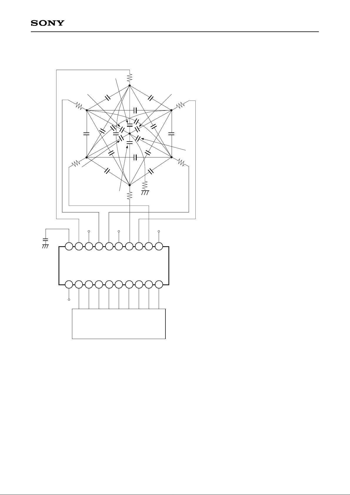
Measurement Circuit
1 2
3 4 5 6 7 8 9 10
111213
14
151617181920
CXD3400N
Between vertical transfer clock and GND C
1 3300pF
Capacitance between vertical transfer clocks C
2 560pF
Capacitance between substrate clock and GND C
3 820pF
Vertical transfer clock series resistor R
1 30Ω
Vertical transfer clock ground resistor R
2 10Ω
–7.5V
C
3
R1
C2
C2
C2
C2
C2
C2
C2
C2
C2 C2
C1
C1
C1
C1
C1
C1
C2
C2
C2
C2
C2
R1
R2
R1
R1
R1
R1
3.3V
15V 0V
Timing Generator
Page 7
– 7 –
CXD3400N
Application Circuit
11
12
13
14
15
16
17
18
19
20
1
2
3
4
5
6
7
8
9
10
V2
CCD
from Timing Generator
CXD3400N
V4
V1A
V1B
V3A
V3B
SUB
3.3V
15V
2200p
1M0.1µ
100k
1µ/35V
0.1µ
–7.5V
0.1µ
0.1µ
∗
See with drive circuit of CCD image sensor.
Note with Power-on Sequence
To protect CCD image sensor, rise two power supplies, VL and VH as follows.
Note that rise VDD first.
t1
VM
VH
VL
20%
20%
t2
t2 ≥ t1
Application circuits shown are typical examples illustrating the operation of the devices. Sony cannot assume responsibility for
any problems arising out of the use of these circuits or for any infringement of third party patent and other right due to same.
Page 8
– 8 –
CXD3400N
20PIN SSOP (PLASTIC)
SONY CODE
EIAJ CODE
JEDEC CODE
PACKAGE STRUCTURE
PACKAGE MATERIAL
LEAD TREATMENT
LEAD MATERIAL
PACKAGE MASS
EPOXY RESIN
PALLADIUM PLATING
COPPER ALLOY
0.1g
SSOP-20P-L01
SSOP020-P-0044
0.1 ± 0.1
0.5 ± 0.2
0° to 10°
DETAIL A
NOTE: Dimension “∗” does not include mold protrusion.
0.15 – 0.01
DETAIL B : PALLADIUM
+ 0.03
b=0.22 ± 0.03
∗6.5 ± 0.1
∗4.4 ± 0.1
0.65
20
11
10
1
A
0.1
1.25 – 0.1
+ 0.2
6.4 ± 0.2
0.13
M
b
Package Outline Unit: mm
 Loading...