

Page 1

Timing Generator for Frame Readout CCD Image Sensor
Description
The CXD3605R is a timing generator IC which
generates the timing pulses for performing frame
readout using the ICX406 CCD image sensor.
Features
• Base oscillation frequency 36MHz
• High-speed/low-speed shutter function
• Supports draft (octuple speed)/AF(auto focus) drive
• Horizontal driver for CCD image sensor
• Vertical driver for CCD image sensor
Applications
Digital still cameras
Structure
Silicon gate CMOS IC
Applicable CCD Image Sensors
ICX406 (Type 1/1.8, 3980K pixels)
Pin Configuration
Absolute Maximum Ratings
• Supply voltage VDD VSS – 0.3 to +7.0 V
VL –10.0 to VSS V
VH VL – 0.3 to +26.0 V
• Input voltage VI VSS – 0.3 to VDD + 0.3 V
• Output voltage VO1 VSS – 0.3 to VDD + 0.3 V
VO2 VL – 0.3 to VSS + 0.3 V
VO3 VL – 0.3 to VH + 0.3 V
• Operating temperature
Topr –20 to +75 °C
• Storage temperature
Tstg –55 to +150 °C
Recommended Operating Conditions
• Supply voltage VDDb 3.0 to 5.25 V
VDDa, VDDc, VDDd 3.0 to 3.6 V
VM 0.0 V
VH 14.55 to 15.45 V
VL –7.0 to –8.0 V
• Operating temperature
Topr –20 to +75 °C
∗
Groups of pins enclosed in the figure indicate
sections for which power supply separation is
possible.
– 1 –
E00Z48
Sony reserves the right to change products and specifications without prior notice. This information does not convey any license by
any implication or otherwise under any patents or other right. Application circuits shown, if any, are typical examples illustrating the
operation of the devices. Sony cannot assume responsibility for any problems arising out of the use of these circuits.
CXD3605R
48 pin LQFP (Plastic)
1 2
3 4 5 6 7 8 9 10
11 12
13
14
15
16
17
18
19
20
21
22
23
24
25
262728
29
30
31
323334
35
36
37
38
39
40
41
42
43
44
45
46
47
48
H2
V
DD3
V
DD4
XSHP
XSHD
XRS
PBLK
CLPDM
V
SS4
OBCLP
ADCLK
V
SS5
CKO
CKI
OSCO
OSCI
V
DD5
MCKO
SSI
SCK
SEN
VD
HD
V
SS6
H1
V
SS3VSS2
RG
VDD2
SSGSL
V
DD1
WEN
ID/EXP
SNCSL
RST
V
SS1
TEST2
SUB
V3B
VL
V3A
V1B
VH
V1A
V4
V2
VM
TEST1
Page 2

– 2 –
CXD3605R
Block Diagram
35 34
39
44
43
41
5
4
24
23
22
20
19
21
181716
15
10
9
81113
12
14
28
27
26
25
30
V1B
V2
V3A
V1A
WEN
ID/EXP
V
SS5
ADCLK
OBCLP
CLPDM
PBLK
VSS4
XRS
XSHD
XSHP
VDD4
V
SS2
RG
V
DD2
V
SS3
H2
H1
V
DD3
VD
HD
7 29 1
VSS136VSS6
V
DD5VDD1
MCKO
CKO
CKI
OSCO
OSCI
Pulse Generator
2
37
48
TEST2
TEST1
RST
45
38
42
47
40
46
VL
VM
VH
SUB
V4
V3B
31
32
33
SEN
SCK
SSI
Register
V Driver
6
SSGSL
3
SNCSL
1/2
1/2
Selector
Selector
Selector
Latch
SSG
Page 3

– 3 –
CXD3605R
Pin Description
GND
Internal system reset input. High: Normal operation, Low: Reset control
Normally apply reset during power-on. Schmitt trigger input
Control input used to switch sync system. High: CKI sync, Low: MCKO sync
With pull-down resistor
Vertical direction line identification pulse output/exposure time identification pulse
output. Switching possible using the serial interface data. (Default: ID)
Memory write timing pulse output.
Internal SSG enable. High: Internal SSG valid, Low: External sync valid.
With pull-down resistor
3.3V power supply. (Power supply for common logic block)
3.3V power supply. (Power supply for RG)
CCD reset gate pulse output.
GND
GND
CCD horizontal register clock output.
CCD horizontal register clock output.
3.3 to 5.0V power supply. (Power supply for H1/H2)
3.3V power supply. (Power supply for CDS block)
CCD precharge level sample-and-hold pulse output.
CCD data level sample-and-hold pulse output.
Sample-and-hold pulse output for analog/digital conversion phase alignment.
Pulse output for horizontal and vertical blanking period pulse cleaning.
CCD dummy signal clamp pulse output.
GND
CCD optical black signal clamp pulse output.
The horizontal/vertical OB pattern can be changed using the serial interface data.
Clock output for analog/digital conversion IC.
Logical phase adjustment possible using the serial interface data.
GND
Inverter output.
Inverter input.
Inverter output for oscillation. When not used, leave open or connect a capacitor.
Inverter input for oscillation. When not used, fix low.
3.3V power supply. (Power supply for common logic block)
System clock output for signal processing IC.
1
2
3
4
5
6
7
8
9
10
11
12
13
14
15
16
17
18
19
20
21
22
23
24
25
26
27
28
29
30
VSS1
RST
SNCSL
ID/EXP
WEN
SSGSL
VDD1
VDD2
RG
VSS2
VSS3
H1
H2
VDD3
VDD4
XSHP
XSHD
XRS
PBLK
CLPDM
V
SS4
OBCLP
ADCLK
V
SS5
CKO
CKI
OSCO
OSCI
V
DD5
MCKO
—
I
I
O
O
I
—
—
O
—
—
O
O
—
—
O
O
O
O
O
—
O
O
—
O
I
O
I
—
O
Pin
No.
Symbol I/O
Description
Page 4

– 4 –
CXD3605R
Serial interface data input for internal mode settings.
Schmitt trigger input
Serial interface clock input for internal mode settings.
Schmitt trigger input
Serial interface strobe input for internal mode settings.
Schmitt trigger input
Vertical sync signal input/output.
Horizontal sync signal input/output.
GND
IC test pin 1; normally fixed to GND. With pull-down resistor
GND (GND for vertical driver)
CCD vertical register clock output.
CCD vertical register clock output.
CCD vertical register clock output.
15.0V power supply. (Power supply for vertical driver)
CCD vertical register clock output.
CCD vertical register clock output.
–7.5V power supply.(Power supply for vertical driver)
CCD vertical register clock output.
CCD electronic shutter pulse output.
IC test pin 2; normally fixed to GND. With pull-down registor
31
32
33
34
35
36
37
38
39
40
41
42
43
44
45
46
47
48
SSI
SCK
SEN
VD
HD
VSS6
TEST1
VM
V2
V4
V1A
VH
V1B
V3A
VL
V3B
SUB
TEST2
I
I
I
I/O
I/O
—
I
—
O
O
O
—
O
O
—
O
O
I
Pin
No.
Symbol I/O
Description
Page 5

– 5 –
CXD3605R
Electrical Characteristics
DC Characteristics (Within the recommended operating conditions)
VDD2
VDD3
VDD4
VDD1, VDD5
RST, SSI, SCK,
SEN
TEST1, TEST2,
SNCSL, SSGSL
VD, HD
H1, H2
RG
XSHP, XSHD,
XRS, PBLK,
OBCLP, CLPDM,
ADCLK
CKO
MCKO
ID/EXP,
WEN
V1A, V1B,
V3A, V3B,
V2, V4
SUB
VDDa
VDDb
VDDc
VDDd
Vt+
Vt–
VIH1
VIL1
VIH2
VIL2
VOH1
VOL1
VOH2
VOL2
VOH3
VOL3
VOH4
VOL4
VOH5
VOL5
VOH6
VOL6
VOH7
VOL7
IOL
IOM1
IOM2
IOH
IOSL
IOSH
3.0
3.0
3.0
3.0
0.8VDDd
0.7VDDd
0.8VDDd
VDDd – 0.8
VDDb – 0.8
VDDa – 0.8
VDDc – 0.8
VDDd – 0.8
VDDd – 0.8
V
DDd – 0.8
10.0
5.0
5.4
3.3
3.3
3.3
3.3
3.6
5.25
3.6
3.6
0.2V
DDd
0.2VDDd
0.2VDDd
0.4
0.4
0.4
0.4
0.4
0.4
0.4
–5.0
–7.2
–4.0
V
V
V
V
V
V
V
V
V
V
V
V
V
V
V
V
V
V
V
V
V
V
V
V
mA
mA
mA
mA
mA
mA
Feed current where IOH = –1.2mA
Pull-in current where IOL = 2.4mA
Feed current where IOH = –22.0mA
Pull-in current where IOL = 14.4mA
Feed current where IOH = –3.3mA
Pull-in current where IOL = 2.4mA
Feed current where IOH = –3.3mA
Pull-in current where IOL = 2.4mA
Feed current where IOH = –6.9mA
Pull-in current where IOL = 4.8mA
Feed current where IOH = –3.3mA
Pull-in current where IOL = 2.4mA
Feed current where IOH = –2.4mA
Pull-in current where IOL = 4.8mA
V1A/B, V2, V3A/B, V4 = –8.25V
V1A/B, V2, V3A/B, V4 = –0.25V
V1A/B, V3A/B = 0.25V
V1A/B, V3A/B = 14.75V
SUB = –8.25V
SUB = 14.75V
Supply
voltage 1
Supply
voltage 2
Supply
voltage 3
Supply
voltage 4
Input
voltage 1
∗1
Input
voltage 2
∗2
Input/output
voltage
Output
voltage 1
Output
voltage 2
Output
voltage 3
Output
voltage 4
Output
voltage 5
Output
voltage 6
Output
current 1
Output
current 2
Item Pins
Symbol
Conditions Min. Typ. Max. Unit
∗1
This input pin is a schmitt trigger input.
∗2
This input pin is with pull-down registor in the IC.
Note) The above table indicates the condition for 3.3V drive.
Page 6

– 6 –
CXD3605R
Inverter I/O Characteristics for Oscillation (Within the recommended operating conditions)
Item
Logical Vth
Input voltage
Output
voltage
Feedback
resistor
Oscillation
frequency
Pins
OSCI
OSCI
OSCO
OSCI, OSCO
OSCI, OSCO
Symbol
LVth
VIH
VIL
VOH
VOL
RFB
f
Conditions
Feed current where IOH = –3.6mA
Pull-in current where IOL = 2.4mA
VIN = VDDd or VSS
Min.
0.7VDDd
VDDd – 0.8
500k
20
Typ.
VDDd/2
2M
Max.
0.3VDDd
0.4
5M
50
Unit
V
V
V
V
V
Ω
MHz
Item
Logical Vth
Input voltage
Input amplitude
Pins
CKI
Symbol
LVth
VIH
VIL
VIN
Conditions
fmax 50MHz sine wave
Min.
0.7VDDd
0.3
Typ.
VDDd/2
Max.
0.3VDDd
Unit
V
V
V
Vp-p
Item
Rise time
Fall time
Output noise voltage
Symbol
TTLM
TTMH
TTLH
TTML
TTHM
TTHL
VCLH
VCLL
VCMH
VCML
Conditions
VL to VM
VM to VH
VL to VH
VM to VL
VH to VM
VH to VL
Min.
200
200
30
200
200
30
Typ.
350
350
60
350
350
60
Max.
500
500
90
500
500
90
1.0
1.0
1.0
1.0
Unit
ns
ns
ns
ns
ns
ns
V
V
V
V
Inverter Input Characteristics for Base Oscillation Clock Duty Adjustment
(Within the recommended operating conditions)
Note) Input voltage is the input voltage characteristics for direct input from an external source. Input amplitude
is the input amplitude characteristics in the case of input through a capacitor.
Switching Characteristics (VH = 15.0V, VM = GND, VL = –7.5V)
Note)
1) The MOS structure of this IC has a low tolerance for static electricity, so full care should be given for
measures to prevent electrostatic discharge.
2) For noise and latch-up countermeasures, be sure to connect a by-pass capacitor (0.1µF or more) between
each power supply pin (VH, VL) and GND.
3) To protect the CCD image sensor, clamp the SUB pin output at VH before input to the CCD image sensor.
Page 7

– 7 –
CXD3605R
Switching Waveforms
V1A (V1B, V3A, V3B)
V2 (V4)
SUB
TTMH TTHM
VH
VM
VL
VM
VL
VH
VL
90%
10%
90%
10%
TTLM
TTLM
90%
10%
90%
10%
TTLH TTHL
90%90%
10% 10%
TTML
90%
10%
TTML
90%
10%
Waveform Noise
VCMH
VCML
VM
VL
VCLH
VCLL
Page 8

– 8 –
CXD3605R
Measurement Circuit
1 2
3 4 5 6 7 8 9 10
11 12
13
14
15
16
17
18
19
20
21
22
23
24
25
262728
29
30
31
323334
35
36
37
38
39
40
41
42
43
44
45
46
47
48
VD
CKI
C6
C6
C6
C6
C6
C6
C6
C6
C6
C5
C5C4
C3
CXD3605R
Serial interface data
HD
+3.3V
–7.5V
+15.0V
C2
C2 C2
C2
C2
R1
R1
R1
R2
R1
R1 R1
C2
C2
C2
C2
C2
C2
C2
C2
C2
C1
C1
C1
C1
C1
C1
C2
C1 3300pF C2 560pF C3 820pF C4 8pF C5 215pF C6 10pF
R1 30Ω R2 10Ω
Page 9

– 9 –
CXD3605R
AC Characteristics
AC characteristics between the serial interface clocks
SSI
0.2VDDd
0.2VDDd
0.8V
DDd
ts2
th1ts1
ts3
0.8V
DDd
0.8V
DDd
SCK
SEN
SEN
Symbol
ts1
th1
ts2
ts3
Definition
SSI setup time, activated by the rising edge of SCK
SSI hold time, activated by the rising edge of SCK
SCK setup time, activated by the rising edge of SEN
SEN setup time, activated by the rising edge of SCK
Min. Typ. Max.
20
20
20
20
Unit
ns
ns
ns
ns
Serial interface clock internal loading characteristics (1)
(Within the recommended operating conditions)
th1
Enlarged view
Example: During frame mode
0.2V
DDd
ts1
0.2V
DDd
V1A
VD
HD
HD
V1A
SEN
0.8V
DDd
Symbol
ts1
th1
Definition
SEN setup time, activated by the falling edge of HD
SEN hold time, activated by the falling edge of HD
Min. Typ. Max.
0
110
Unit
ns
µs
∗
Be sure to maintain a constantly high SEN logic level near the falling edge of the HD in the horizontal period
during which V1A/B and V3A/B values take the ternary value and during that horizontal period.
(Within the recommended operating conditions)
Page 10

– 10 –
CXD3605R
Serial interface clock output variation characteristics
Normally, the serial interface data is loaded to the CXD3605R at the timing shown in "Serial interface clock
internal loading characteristics (1)" above. However, one exception to this is when the data such as STB is
loaded to the CXD3605R and controlled at the rising edge of SEN. See "Description of Operation".
0.8VDDd
SEN
Output signal
tpdPULSE
Symbol
tpdPULSE
Definition
Output signal delay, activated by the rising edge of SEN
Min. Typ. Max.
1005
Unit
ns
(Within the recommended operating conditions)
Serial interface clock internal loading characteristics (2)
th1
0.2V
DDd
ts1
0.2VDDd
VD
HD
VD
HD
SEN
0.8V
DDd
Enlarged view
Example: During frame mode
Symbol
ts1
th1
Definition
SEN setup time, activated by the falling edge of VD
SEN hold time, activated by the falling edge of VD
Min. Typ. Max.
0
200
Unit
ns
ns
∗
Be sure to maintain a constantly high SEN logic level near the falling edge of VD.
(Within the recommended operating conditions)
Page 11

– 11 –
CXD3605R
RST
0.2VDDd
tw1
0.8VDDd
VD
HD
ts1
th1
0.2V
DDd
0.2V
DDd
0.2V
DDd
RST loading characteristics
Symbol
tw1
Definition
RST pulse width
Min. Typ. Max.25Unit
ns
(Within the recommended operating conditions)
VD and HD phase characteristics
Symbol
ts1
th1
Definition
VD setup time, activated by the falling edge of HD
VD hold time, activated by the falling edge of HD
Min. Typ. Max.
20
100
Unit
ns
ns
(Within the recommended operating conditions)
HD
MCKO
ts1
th1
0.2V
DDd
0.8V
DDd
0.2VDDd
HD loading characteristics
Symbol
ts1
th1
Definition
HD setup time, activated by the rising edge of MCKO
HD hold time, activated by the rising edge of MCKO
Min. Typ. Max.
20
5
Unit
ns
ns
MCKO load capacitance = 10pF
(Within the recommended operating conditions)
Page 12

– 12 –
CXD3605R
0.8VDDd
MCKO
WEN, ID/EXP
tpd1
WEN and ID/EXP load capacitance = 10pF
(Within the recommended operating conditions)
Symbol
tpd1
Definition
Time until the above outputs change after the rise of MCKO
Min. Typ. Max.
6020
Unit
ns
Output variation characteristics
Page 13

– 13 –
CXD3605R
Description of Operation
Pulses output from the CXD3605R are controlled mainly by the RST pin and by the serial interface data. The
Pin Status Table is shown below, and the details of serial interface control are described on the following
pages.
Pin Status Table
∗1
It is for output. For input, all items are "ACT".
Note) ACT means that the circuit is operating, and DIS means that loading is stopped. L indicates a low
output level, and H a high output level in the controlled status.
Also, VH, VM and VL indicate the voltage levels applied to VH (Pin 42), VM (Pin 38) and VL (Pin 45),
respectively, in the controlled status.
Pin
No.
1
2
3
4
5
6
7
8
9
10
11
12
13
14
15
16
17
18
19
20
21
22
23
24
VSS1
RST
SNCSL
ID/EXP
WEN
SSGSL
VDD1
VDD2
RG
VSS2
VSS3
H1
H2
VDD3
VDD4
XSHP
XSHD
XRS
PBLK
CLPDM
VSS4
OBCLP
ADCLK
VSS5
ACT
ACT
ACT
ACT
ACT
ACT
ACT
ACT
ACT
ACT
ACT
ACT
ACT
ACT
ACT
ACT
ACT
L
L
ACT
L
L
L
L
L
L
L
L
L
L
ACT
ACT
L
L
ACT
L
L
L
L
L
L
L
L
L
L
L
ACT
L
L
ACT
ACT
ACT
ACT
ACT
ACT
ACT
H
H
H
ACT
25
26
27
28
29
30
31
32
33
34
35
36
37
38
39
40
41
42
43
44
45
46
47
48
CKO
CKI
OSCO
OSCI
VDD5
MCKO
SSI
SCK
SEN
VD
∗1
HD
∗1
VSS6
TEST1
VM
V2
V4
V1A
VH
V1B
V3A
VL
V3B
SUB
TEST2
ACT
ACT
ACT
ACT
ACT
ACT
ACT
ACT
ACT
ACT
ACT
ACT
ACT
ACT
ACT
ACT
ACT
ACT
ACT
ACT
ACT
ACT
ACT
ACT
ACT
L
L
VM
VM
VH
VH
VH
VH
VH
L
ACT
ACT
ACT
L
ACT
ACT
ACT
L
L
VM
VM
VH
VH
VH
VH
VH
ACT
ACT
ACT
ACT
ACT
DIS
DIS
DIS
H
H
VM
VL
VM
VM
VL
VL
VL
Symbol CAM SLP STB RST
Pin
No.
Symbol CAM SLP STB RST
—
—
—
—
—
—
—
—
—
—
—
—
—
—
—
—
Page 14
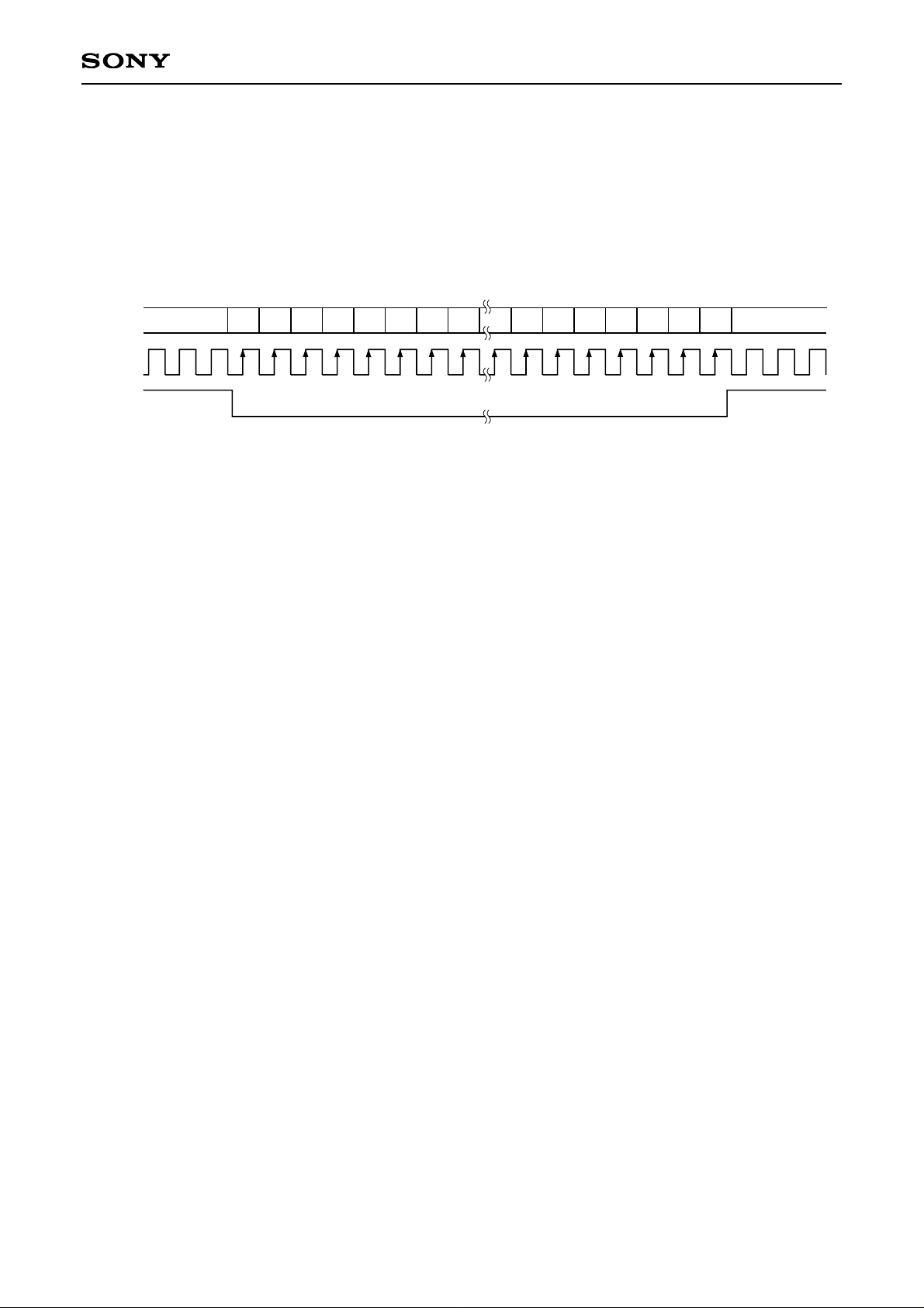
– 14 –
CXD3605R
Serial Interface Control
The CXD3605R basically loads and reflects the serial interface data sent in the following format in the readout
portion at the falling edge of HD. Here, readout portion specifies the horizontal period during which V1A/B and
V3A/B, etc. take the ternary value.
Note that some items reflect the serial interface data at the falling edge of VD or the rising edge of SEN.
SSI
SCK
SEN
00 01 02 03 04 05 06 07 41 42 43 44 45 46 47
These are two categories of serial interface data: the CXD3605R drive control data (hereafter "control data")
and electronic shutter data (hereafter "shutter data").
The details of each data are described below.
Page 15
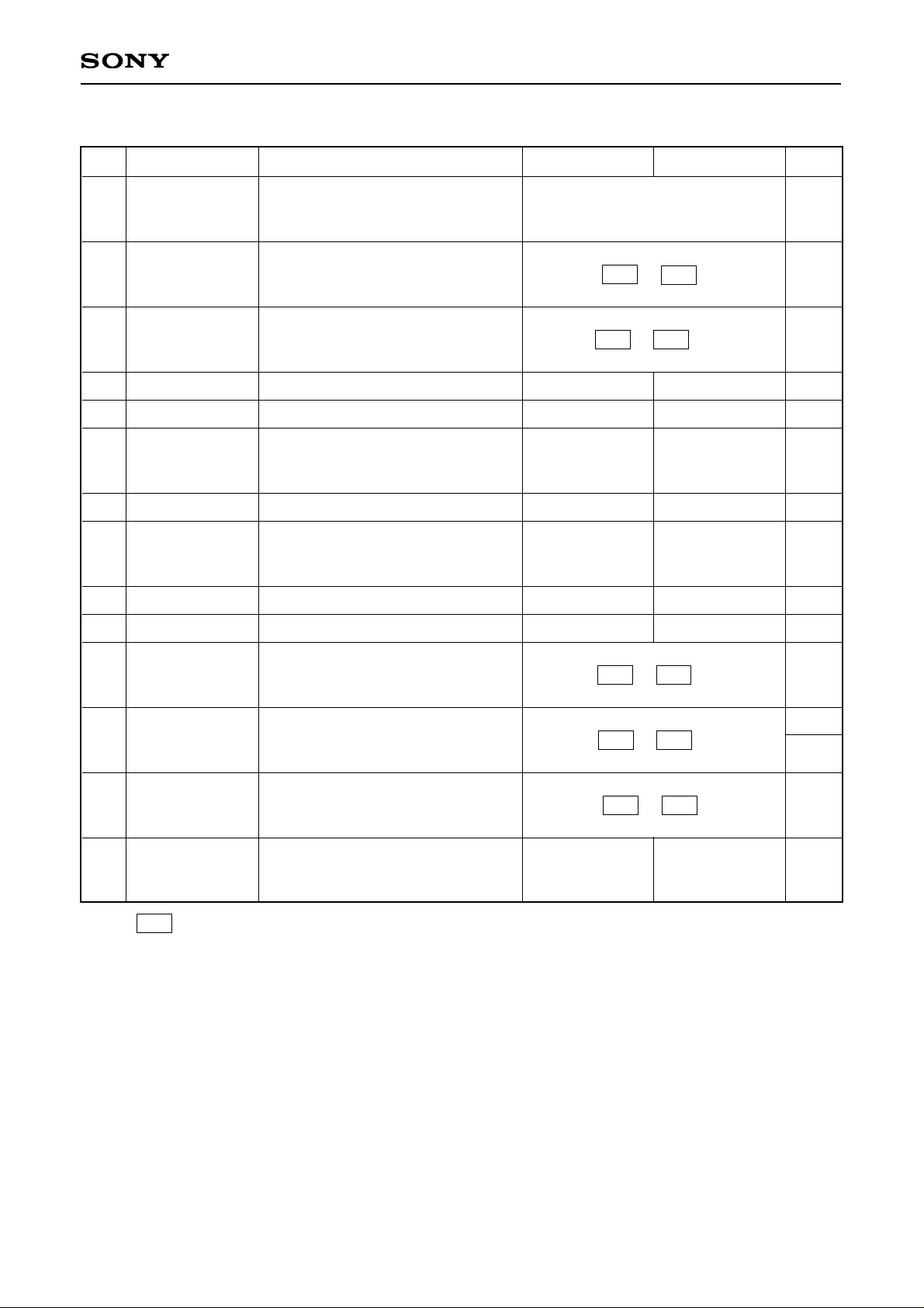
– 15 –
CXD3605R
Control Data
Data
D00
to
D07
D08
to
D09
D10
to
D12
D13
D14
D15
to
D16
D17
D18
to
D31
D32
D33
D34
to
D35
D36
to
D37
D38
to
D39
D40
to
D47
Symbol
CHIP
CTG
MODE
SMD
HTSG
—
NTPL
—
FGOB
EXP
PTOB
LDAD
STB
—
Function
Chip enable
Category switching
Drive mode switching
Electronic shutter mode switching
∗1
HTSG control switching
∗1
—
SSG function switching
—
Wide OBCLP generation switching
ID/EXP output switching
OBCLP waveform patterm switching
ADCLK logic phase adjustment
Standby control
—
Data = 0 Data = 1
10000001 → Enabled
Other values → Disabled
See D08 to D09 CTG.
See D10 to D12 MODE.
OFF ON
OFF ON
——
NTSC PAL
——
OFF ON
ID EXP
See D34 to D35 PTOB.
See D36 to D37 LDAD.
See D38 to D39 STB.
——
RST
All
0
All
0
All
0
0
0
All
0
0
All
0
0
0
All
0
1
0
All
0
All
0
∗1
See D13 SMD.
Page 16

– 16 –
CXD3605R
Shutter Data
Data
D00
to
D07
D08
to
D09
D10
to
D19
D20
to
D31
D32
to
D41
D42
to
D47
Symbol
CHIP
CTG
SVD
SHD
SPL
—
Function
Chip enable
Category switching
Electronic shutter vertical period
specification
Electronic shutter horizontal period
specification
High-speed shutter position
specification
—
Data = 0 Data = 1
10000001 → Enabled
Other values → Disabled
See D08 to D09 CTG.
See D10 to D19 SVD.
See D20 to D31 SHD.
See D32 to D41 SPL.
——
RST
All
0
All
0
All
0
All
0
All
0
All
0
Page 17

– 17 –
CXD3605R
Detailed Description of Each Data
Shared data: D08 to D09 CTG [Category]
Of the data provided to the CXD3605R by the serial interface, the CXD3605R loads D10 and subsequent
data to each data register as shown in the table below according to the combination of D08 and D09 .
D09
0
0
1
D08
0
1
X
Description of operation
Loading to control data register
Loading to shutter data register
Test mode
D11
0
0
1
1
D12
0
0
0
0
D10
0
1
0
1
D11
0
0
1
1
D12
1
1
1
1
D10
0
1
0
1
Description of operation Description of operation
Draft mode (default)
AF1 mode
AF2 mode
Frame mode
Draft mode
Frame mode (A field read out)
Frame mode (B field read out)
Test mode
Note that the CXD3605R can apply these categories consecutively within the same vertical period. However,
care should be taken as the data is overwritten if the same category is applied.
Control data: D10 to D12 MODE [Drive mode]
The CXD3605R drive mode can be switched as follows. However, the drive mode bits are located to the
CXD3605R and reflected at the falling edge of VD.
Draft mode is the pulse eliminator drive mode called octuple speed mode in the ICX406. This is a high frame
rate drive mode that can be used for purposes such as monitoring and auto focus (AF).
AF1 and AF2 modes are the pulse eliminator drive modes called by the same names in the ICX406. These
drive modes are based on draft mode, and are used to increase the frame rate for auto focus (AF). In these
modes, the screen is swept in the vertical direction and the center portion lines are cut out.
Frame mode is the ICX406 drive mode in which the data for all lines are read. This drive mode is comprised of
A and B Fields, so when it is established, repeated drive is performed in the manner of A → B → A → and so
on.
Frame mode (A or B Field) is the drive mode in which each field can be specified separately.
Control data: D17 NTPL [SSG function switching]
The CXD3605R internal SSG output pattern can be switched as follows. However, the SSG function switching
bits are loaded to the CXD3605R and reflected at the falling edge of VD.
D17
0
1
Description of Operation
NTSC equivalent pattern output
PAL equivalent pattern output
VD period in each pattern is defined as follows.
See the Timing Charts for the actual operation.
NTSC equivalent pattern
PAL equivalent pattern
Frame mode
1012H + 1672ck
944H + 464ck
Draft mode
224H + 1372ck × 2
269H + 2039ck
AF1 mode
112H + 1372ck
134H + 2354ck
AF2 mode
56H + 686ck
67H + 1178ck
Page 18

– 18 –
CXD3605R
Control data: D32 FGOB [Wide OBCLP generation]
This controls wide OBCLP generation during the vertical OPB period. See the Timing Charts for the actual
operation. The default is "OFF".
D32
0
1
Description of operation
Wide OBCLP generation OFF
Wide OBCLP generation ON
Control data: D34 to D35 PTOB [OBCLP waveform pattern]
This indicates the OBCLP waveform pattern. The default is "Normal".
D35
0
0
1
1
D34
0
1
0
1
Waveform pattern
(Normal)
(Shifted rearward)
(Shifted forward)
(Wide)
Control data: D36 to D37 LOAD [ADCLK logical phase]
This indicates the ADCLK logic phase adjustment data. The default is 90° relative to MCKO.
D37
0
0
1
1
D36
0
1
0
1
Degree of adjustment (°)
0
90
180
270
Control data: D38 to D39 STB [Standby]
The operating mode is switched as follows. However, the standby bits are loaded to the CXD3605R and
control is applied immediately at the rising edge of SEN.
D39
X
0
1
D38
0
1
1
Symbol
CAM
SLP
STB
Operating mode
Normal operating mode
Sleep mode
Standby mode
See the Pin Status Table for the pin status in each mode.
Page 19

– 19 –
CXD3605R
Control data/shutter data: [Electronic shutter]
The CXD3605R realizes various electronic shutter functions by using control data D13 SMD and D14 HTSG
and shutter data D10 to D19 SVD, D20 to D31 SHD and D32 to D41 SPL.
These functions are described in detail below.
First, the various modes are shown below.
These modes are switched using control data D13 SMD.
D13
0
1
Description of operation
Electronic shutter stopped mode
Electronic shutter mode
The electronic shutter data is expressed as shown in the table below using D20 to D31 SHD as an example.
However, MSB (D31) is a reserve bit for the future specification, and it is handled as a dummy on this IC.
MSB LSB
D29 D28D31 D30 D27 D26 D25 D24 D23 D22 D21 D20
1100
↓
C
X001
↓
1
0011
↓
3
SHD is expressed as 1C3h .
[Electronic shutter stopped mode]
During this mode, all shutter data items are invalid.
SUB is not output in this mode, so the shutter speed is the accumulation time for one field.
[Electronic shutter mode]
During this mode, the shutter data items have the following meanings.
Note) The bit data definition area is assured in terms of the CXD3605R functions, and does not assure the
CCD characteristics.
The period during which SVD and SHD are specified together is the shutter speed. An image of the exposure
time calculation formula is shown below. In actual operation, the precise exposure time is calculated from the
operating frequency, VD and HD periods, decoding value during the horizontal period, and other factors.
(Exposure time) = SVD + {(number of HD per 1V) – (SHD + 1)}
Concretely, when specifying high-speed shutter, SVD is set to "000h". (See the figure.) During low-speed
shutter, or in other words when SVD is set to "001h" or higher, the serial interface data is not loaded until this
period is finished.
The vertical period indicated here corresponds to one field in each drive mode. In addition, the number of
horizontal periods applied to SHD can be considered as (number of SUB pulses – 1).
Symbol
SVD
SHD
SPL
Data
D10 to D19
D20 to D31
D32 to D41
Description
Number of vertical periods specification (000h ≤ SVD ≤ 3FFh)
Number of horizontal periods specification (000h ≤ SHD ≤ 7FFh)
Vertical period specification for high-speed shutter operation (000h ≤ SPL ≤ 3FFh)
Page 20

– 20 –
CXD3605R
VD
SHD
1
V1A
SUB
WEN
SMD
000h
002h
SVD
050h
10Fh
SHD
1
SVD
EXP
Exposure time
VD
SPL
001 002000
SHD
1
V1A
SUB
WEN
SMD
000h
001h
SPL
000h
002h
SVD
0A3h
10Fh
SHD
EXP
Exposure time
1
SVD
Further, SPL can be used during this mode to specify the SUB output at the desired vertical period during the
low-speed shutter period.
In the case below, SUB is output based on SHD at the SPL vertical period out of (SVD + 1) vertical periods.
Incidentally, SPL is counted as "000h", "001h", "002h" and so on in conformance with SVD.
Using this function it is possible to achieve smooth exposure time transitions when changing from low-speed
shutter to high-speed shutter or vice versa.
Page 21

– 21 –
CXD3605R
VD
V1A
SUB
WEN
0
1
0
HTSG
1
0
1
SMD
Vck
Exposure time
EXP
[HTSG control mode]
This mode controls the V1A/B and V3A/B ternary level outputs (readout pulse block) using D14 HTSG.
D14
0
1
Description of operation
Readout pulse (SG) normal operation
HTSG control mode
[EXP pulse]
The ID/EXP pin (Pin 4) output can be switched between the ID pulse or the EXP pulse using D33 EXP. The
default is the "ID" pulse. See the Timing Charts for the ID pulse. The EXP pulse indicates the exposure time
when it is high. The transition point is the last SUB pulse falling edge, and midpoint value (1338ck) of each
V1A/B and V3A/B ternary out put falling edge. When there is no SUB pulse, the later ternary output falling
edge (1416ck) is used. See the EXP pulse indicated in the explanatory diagrams under [Electronic shutter] for
an image of operation.
Note that the above specification is based on draft mode. For frame mode, the former value is 1260ck and the
latter value is 1416ck.
Page 22

– 22 –
CXD3605R
VD
SUB
OBCLP
CLPDM
V1ACCV1B
V2
V3A
V3B
V4
CCD OUT
1547
1719
1712
1714
1716
1718
1720
1709
1711
1713
1715
3
1
57
246810
2
12
4689111357911
PBLK
ID/EXP
WEN
A Field B Field
HD
1
75 82
174821013943 9431013
A B
High-speed sweep block High-speed sweep block
∗
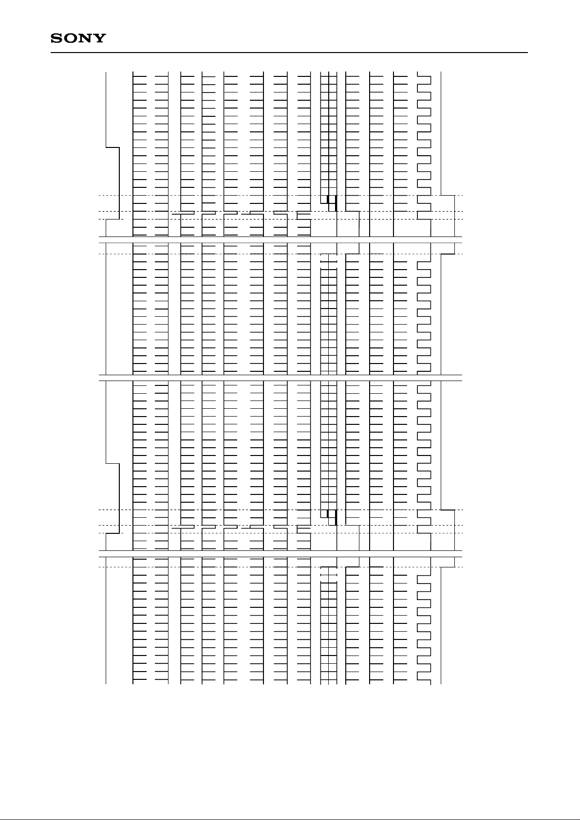
The number of SUB pulses is determined by the serial interface data. This chart shows the case where SUB pulses are output in each horizontal period.
∗
ID/EXP of this chart shows ID. ID is low for lines where CCD OUT contains the R component, and high for lines where CCD OUT contains the B component.
∗
VD of this chart is NTSC equivalent pattern (1012H + 1672ck units). For PAL equivalent pattern, it is 944H + 464ck units.
Chart-1 Vertical Direction Timing Chart
MODE
Frame mode
Applicable CCD image sensor
• ICX406
Page 23
– 23 –
CXD3605R
VD
HD
SUB
V1A
V2
V3A
V3B
V4
OBCLP
CLPDM
ID/EXP
PBLK
V1B
CCD OUT
145
10
21 30 37
101
61
17 26 33
46
42
5
10
14 21 30 37
1
6
1
10 17 26 33
46
42
WEN
3
1
218
3
1218
D D
1717
1710
1713
1706
1717
1710
1713
1706
226226
∗
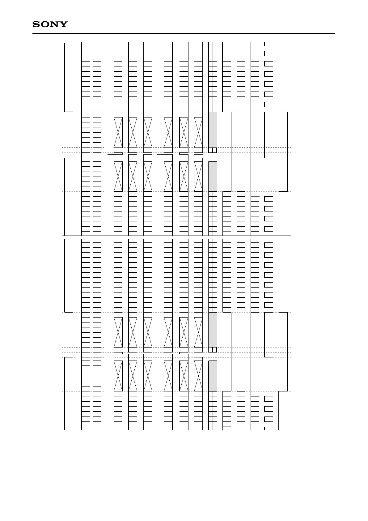
The number of SUB pulses is determined by the serial interface data. This chart shows the case where SUB pulses are output in each horizontal period.
∗
ID/EXP of this chart shows ID. ID is low for lines where CCD OUT contains the R component, and high for lines where CCD OUT contains the B component.
∗
VD of this chart is NTSC equivalent pattern (224H + 1372ck + 1372ck units). For PAL equivalent pattern, it is 269H + 2039ck units.
Chart-2 Vertical Direction Timing Chart
MODE
Draft mode
Applicable CCD image sensor
• ICX406
Page 24
– 24 –
CXD3605R
VD
SUB
OBCLP
CLPDM
V1A
V1B
V2
V3A
V3B
V4
CCD OUT
PBLK
ID/EXP
WEN
HD
2
9
29106 106
10
6
10
6
E FG GEF
113113
High-speed
sweep block
Frame shift block
High-speed
sweep block
Frame shift block
∗
The number of SUB pulses is determined by the serial interface data. This chart shows the case where SUB pulses are output in each horizontal period.
∗
ID/EXP of this chart shows ID. ID is low for lines where CCD OUT contains the R component, and high for lines where CCD OUT contains the B component.
∗
240 stages are fixed for high-speed sweep block; 232 stages are fixed for frame shift block.
∗
VD of this chart is NTSC equivalent pattern (112H + 1372ck units). For PAL equivalent pattern, it is 134H + 2354ck units.
Chart-3 Vertical Direction Timing Chart
MODE
AF1 mode
Applicable CCD image sensor
• ICX406
Page 25

– 25 –
CXD3605R
VD
SUB
OBCLP
CLPDM
V1A
High-speed sweep block
V1B
V2
V3A
V3B
V4
CCD OUT
PBLK
ID/EXP
WEN
HD
2
12
21247 47
10
6
10
6
G G E FE
Frame shift block
High-speed sweep block
Frame shift block
F
57 57
∗
The number of SUB pulses is determined by the serial interface data. This chart shows the case where SUB pulses are output in each horizontal period.
∗
ID/EXP of this chart shows ID. ID is low for lines where CCD OUT contains the R component, and high for lines where CCD OUT contains the B component.
∗
360 stages are fixed for high-speed sweep block; 360 stages are fixed for frame shift block.
∗
VD of this chart is NTSC equivalent pattern (56H + 686ck units). For PAL equivalent pattern, it is 67H + 1178ck units.
Chart-4 Vertical Direction Timing Chart
MODE
AF2 mode
Applicable CCD image sensor
• ICX406
Page 26
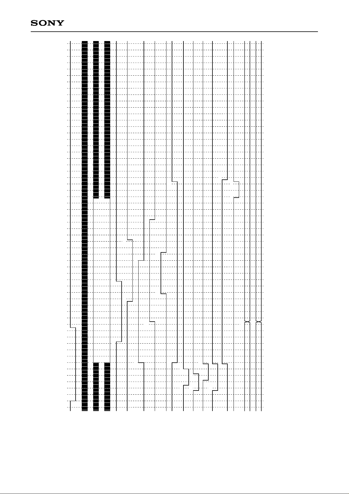
– 26 –
CXD3605R
HD
MCKO
H1
H2
V1A/BV2V3A/B
V4
SUB
PBLK
OBCLP (1)
OBCLP (2)
OBCLP (3)
OBCLP (4)
OBCLP
CLPDM
(2669)
0 50 100 200150 250 300 350 400 450 500 550
ID/EXP
WEN
317 345 361 365
604
18892
5024
4216
5816
34758
5832
343319
252156
22060
34360
284124
232168
124
124
∗
The HD of this chart indicates the actual CXD3605R load timing.
∗
The numbers at the output pulse transition points indicate the count at the MCKO rise from the fall of HD.
∗
The HD fall period should be between approximately 3.3 to 17.6µs (when the drive frequency is 18MHz). This chart shows a period of 115ck (6.4µs). Internal SSG is at this timing.
∗
SUB is output at the timing shown above when output is controlled by the serial interface data.
∗
ID/EXP of this chart shows ID. ID/EXP and WEN are output at the timing shown above at the position shown in Chart-1.
Chart-5 Horizontal Direction Timing Chart
MODE
Frame mode
Applicable CCD image sensor
• ICX406
Page 27

– 27 –
CXD3605R
HD
MCKO
H1
H2
V1A/BV2V3A/B
V4
SUB
PBLK
OBCLP (1)
OBCLP (2)
OBCLP (3)
OBCLP (4)
OBCLP
CLPDM
(2669)
0 50 100 200150 250 300 350 400 450 500 550
ID/EXP
WEN
317 345 361 365
604
9268
5024
4216
5816
34758
5832
343319
10884
10060
34360
11676
232168
124
124
156132
172148
164124
180140
220196
212
228188
244204
284260
300276
292252
308268
236
∗
The HD of this chart indicates the actual CXD3605R load timing.
∗
The numbers at the output pulse transition points indicate the count at the MCKO rise from the fall of HD.
∗
The HD fall period should be between approximately 3.3 to 17.6µs (when the drive frequency is 18MHz). This chart shows a period of 115ck (6.4µs). Internal SSG is at this timing.
∗
SUB is output at the timing shown above when output is controlled by the serial interface data.
∗
ID/EXP of this chart shows ID. ID/EXP and WEN are output at the timing shown above at the position shown in Chart-2, 3 and 4.
Chart-6 Horizontal Direction Timing Chart
MODE
Draft mode, AF1 mode, AF2 mode
Applicable CCD image sensor
• ICX406
Page 28

– 28 –
CXD3605R
HD
MCKO
H1
H2
V1A/BV2V3A/B
V4
SUB
PBLK
OBCLP
CLPDM
(2669)
0 50 100 200150 250 300 350 400 450 500 550
ID/EXP
WEN
317 345 361 365
604
11660
232168
172 228 284 340 396 452 508 564
11660 172 228 284 340 396 452 508 564
14488 200 256 312 368 424 480 536
14488 200 256 312 368 424 480 536
#4#3#2#1 #5
∗
The HD of this chart indicates the actual CXD3605R load timing.
∗
The numbers at the output pulse transition points indicate the count at the MCKO rise from the fall of HD.
∗
The HD fall period should be between approximately 3.3 to 17.6µs (when the drive frequency is 18MHz). This chart shows a period of 115ck (6.4µs). Internal SSG is at this timing.
∗
SUB is output at the timing shown above when output is controlled by the serial interface data.
∗
ID/EXP of this chart shows ID.
∗
High-speed sweep of V1A/B, V2, V3A/B, V4 is performed up to 72H of 2660ck (#1739).
Chart-7 Horizontal Direction Timing Chart
(High-speed sweep: C)
MODE
Frame mode
Applicable CCD image sensor
• ICX406
Page 29
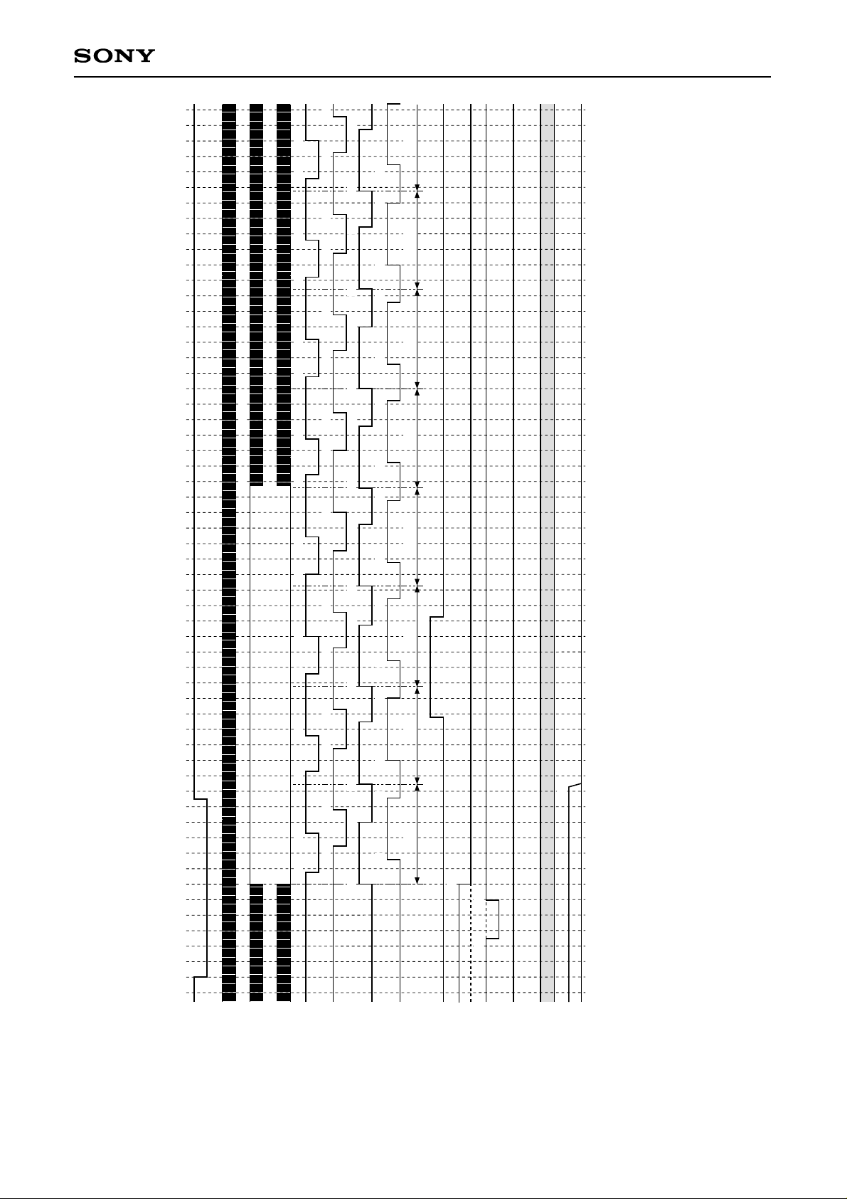
– 29 –
CXD3605R
HD
MCKO
H1
H2
V1A/BV2V3A/B
V4
SUB
PBLK
OBCLP
CLPDM
(2669)
0 50 100 200150 250 300 350 400 450 500 550
ID/EXP
WEN
317 345 361 365
604
232168
60
60
5024
124
100 124 164 188 228 252 292 316 356 380 420 444 484 508 548
108 148 172 212 236 276 300 340 364 404 428 468 492 532 55684
92 132 156 196 220 260 284 324 348 388 412 452 476 516 54068
76 116 140 180 204 244 268 308 332 372 396 436 460 500 524
#6 #7#4 #5#3#1 #2 #8
∗
The HD of this chart indicates the actual CXD3605R load timing.
∗
The numbers at the output pulse transition points indicate the count at the MCKO rise from the fall of HD.
∗
The HD fall period should be between approximately 3.3 to 17.6µs (when the drive frequency is 18MHz). This chart shows a period of 115ck (6.4µs). Internal SSG is at this timing.
∗
SUB is output at the timing shown above when output is controlled by the serial interface data.
∗
ID/EXP of this chart shows ID. PBLK, OBCLP, ID/EXP and WEN are output at the timing shown above at the position shown in Chart-2, 3 and 4.
∗
Frame shift of V1A/B, V2, V3A/B and V4 is performed up to 7H 1563ck (#232) in AF1 mode and 10H 1688ck (#360) in AF2 mode.
In addition, high-speed sweep is performed up to 111H 2015ck (#240) in AF1 mode and 55H 1688ck (#360) in AF2 mode.
Chart-8 Horizontal Direction Timing Chart
(Frame shift: F)
(High-speed sweep: G)
MODE
AF1 mode, AF2 mode
Applicable CCD image sensor
• ICX406
Page 30

– 30 –
CXD3605R
HD
[A Field]
[B Field]
A
B
V3B
V4
V3B
V4
V1A
V1B
V2
V3A
V1A
V1B
V2
V3A
(2669)
0
(2669)
0
1104
1136
1168
1200
1202
1260
1292
124
156
188
220
252
284
∗
The HD of this chart indicates the actual CXD3605R load timing.
∗
The numbers at the output pulse transition points indicate the count at the MCKO rise from the fall of HD.
∗
The HD fall period should be between approximately 3.3 to 17.6µs (when the drive frequency is 18MHz). This chart shows a period of 115ck (6.4µs). Internal SSG is at this timing.
Chart-9 Horizontal Direction Timing Chart
MODE
Frame mode
Applicable CCD image sensor
• ICX406
Page 31

– 31 –
CXD3605R
HD
D
V3B
V4
V1A
V1B
V2
V3A
(2669)
0
(2669)
0
1104
1136
1168
1200
1202
1356
1358
1260
1292
1324
1416
60
76
92
108
124
140
156
172
68
84
100
116
132
148
164
180
∗
The HD of this chart indicates the actual CXD3605R load timing.
∗
The numbers at the output pulse transition points indicate the count at the MCKO rise from the fall of HD.
∗
The HD fall period should be between approximately 3.3 to 17.6µs (when the drive frequency is 18MHz). This chart shows a period of 115ck (6.4µs). Internal SSG is at this timing.
Chart-10 Horizontal Direction Timing Chart
MODE
Draft mode
Applicable CCD image sensor
• ICX406
Page 32

– 32 –
CXD3605R
HD
E
V3B
V4
V1A
V1B
V2
V3A
(2669)
0
(2669)
0
1104
1136
1168
1200
1202
1356
1358
1260
1292
1324
1416
60
76
92
108
124
140
156
172
68
84
100
116
132
148
164
180
188
204
220
236
252
268
284
300
196
212
228
244
260
276
292
308
1448
1464
1480
1496
1512
1528
1544
1560
1456
1472
1488
1504
1520
1536
1552
1568
∗
The HD of this chart indicates the actual CXD3605R load timing.
∗
The numbers at the output pulse transition points indicate the count at the MCKO rise from the fall of HD.
∗
The HD fall period should be between approximately 3.3 to 17.6µs (when the drive frequency is 18MHz). This chart shows a period of 115ck (6.4µs). Internal SSG is at this timing.
Chart-11 Horizontal Direction Timing Chart
MODE
AF1 mode, AF2 mode
Applicable CCD image sensor
• ICX406
Page 33
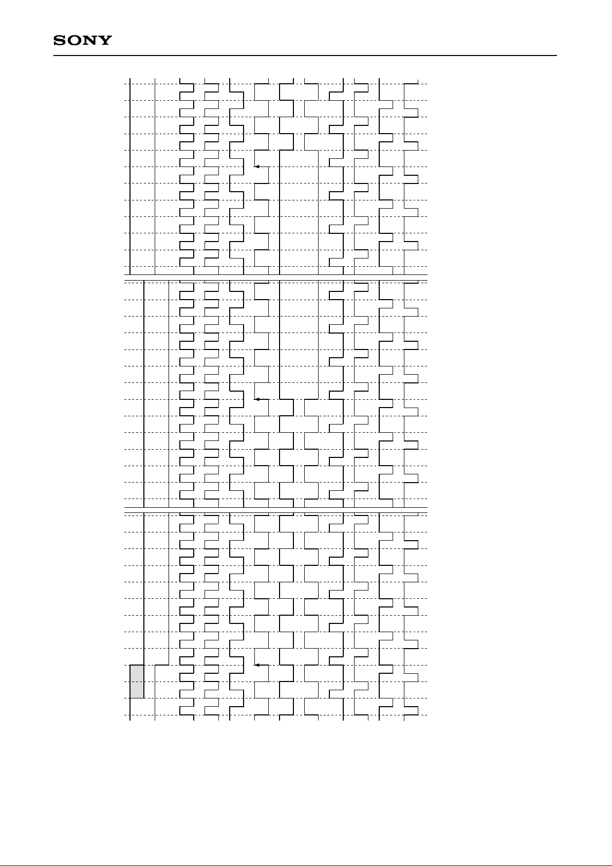
– 33 –
CXD3605R
HD
HD'
CKI
CKO
ADCLK
MCKO
H1
H2
RG
XSHP
XSHD
XRS
317
60
1
∗
HD' indicates the HD which is the actual CXD3605R load timing.
∗
The phase relationship of each pulse shows the logical position relationship. For the actual output waveform, a delay is added to each pulse.
∗
The logical phase of ADCLK can be specified by the serial interface data.
Chart-12 High-Speed Phase Timing Chart
MODE
Applicable CCD image sensor
• ICX406
Page 34

– 34 –
CXD3605R
VD
V1A
V1B
V2
V3A
V3B
V4
SUB
Mechanical
shutter
Exposure
time
CCD OUT
MODE
SMD
SHD
Close Open
ABC
EE
F
00000 3 3 0 0
11111 0 0 1 1
050h 050h 050h 050h 050h 000h 000h 050h 050h
ABCDE F
∗
This chart is a drive timing chart example of electronic shutter normal operation.
∗
Data exposed at D includes the blooming component. For details, see the CCD image sensor data sheet.
∗
The CXD3605R does not generate the pulse to control mechanical shutter operation.
∗
The switching timing of drive mode and electronic shutter data is not the same.
Chart-13 Vertical Direction Sequence Chart
MODE
Draft → Frame → Draft
Applicable CCD image sensor
• ICX406
Page 35

– 35 –
CXD3605R
Application Circuit Block diagram
26 27 37 48 31 32
34
35
30
25
23
22
201918
17
16
MCKO
VD
HD
CKO
D OUT
ADCLK
OBCLP
CLPDM
PBLK
XRS
XSHD
XSHP
SCK
33
SEN
SSI
TEST2
TEST1
OSCO
CKI
28
OSCI
CCD OUT
V-Dr
SSG
6
3
2
5
4
SSGSL
SNCSL
RST
WEN
ID/EXP
12
13
9
RG
H2
H1
41
43
39
V2
V1B
V1A
44
46
40
V4
47
SUB
V3B
V3A
CCD
ICX406
CDS/ADC Block
TG
CXD3605R
Controller
Signal Processor Block
Notes for Power-on
Of the three –7.5V, +15.0V, –3.3V power supplies, be sure to start up the –7.5V and +15.0V power supplies in
the following order to prevent the SUB pin of the CCD image sensor from going to negative potential.
t1
t2
15.0V
0V
–7.5V
20%
20%
t2 ≥ t1
Application circuits shown are typical examples illustrating the operation of the devices. Sony cannot assume responsibility for
any problems arising out of the use of these circuits or for any infringement of third party patent and other right due to same.
Page 36

– 36 –
CXD3605R
Sony Corporation
Package Outline Unit: mm
SONY CODE
EIAJ CODE
JEDEC CODE
PACKAGE MATERIAL
LEAD TREATMENT
LEAD MATERIAL
PACKAGE MASS
EPOXY RESIN
COPPER ALLOY
PACKAGE STRUCTURE
48PIN LQFP (PLASTIC)
9.0 ± 0.2
∗ 7.0 ± 0.1
1
12
13
24
25
36
37
48
(0.22)
0.18 – 0.03
+ 0.08
0.2g
LQFP-48P-L01
P-LQFP48-7x7-0.5
(8.0)
0.5
±
0.2
0.127 – 0.02
+ 0.05
A
1.5 – 0.1
+ 0.2
0.1
PALLADIUM PLATING
NOTE: Dimension “∗” does not include mold protrusion.
0.1 ± 0.1
0.5
±
0.2
0° to 10°
DETAIL A
0.13
M
0.5
S
S
B
DETAIL B: PALLADIUM
0.127
±
0.04
0.18 ± 0.03
 Loading...