

Page 1

Digital Signal Driver/Timing Generator
Description
The CXD3526GG incorporates digital signal
processor type RGB driver, color shading correction and
timing generator functions onto a single IC. Operation is
possible with a system clock up to 85 [MHz] (max.). This
IC can process video signals in bands up to XGA
standard, and can output the timing signals for driving
various Sony LCD panels such as XGA and SVGA.
CXD3526GG
144 pin BGA (Plastic)
Features
• Various picture quality adjustment functions such
as user adjustment, white balance adjustment and
gamma correction
• OSD MIX, black frame processing, mute and
limiter functions
• LCD panel color shading correction function
• Drives various Sony data projector LCD panels
such as XGA and SVGA
• Controls the CXA3562AR and CXA7000R sample-
and-hold drivers
• Line inversion and field inversion signal generation
• Supports AC drive of LCD panels during no signal
• On-chip serial interface
• The data of gamma correction and color shading
correction can be downloaded automatically from
the external EEPROM.
Applications
LCD projectors and other video equipment
Absolute Maximum Ratings (VSS = 0V)
• Supply voltage VDD1 VSS – 0.5 to +3.0 V
VDD2 VSS – 0.5 to +4.0 V
• Input voltage VI VSS – 0.5 to VDD2 + 0.5 V
• Output voltage VO VSS – 0.5 to VDD2 + 0.5 V
• Storage temperature
Tstg –55 to +125 °C
• Junction temperature
Tj 125 °C
Recommended Operating Conditions
• Supply voltage VDD1 2.3 to 2.7 V
VDD2 3.0 to 3.6 V
• Operating temperature
Topr –20 to +75 °C
Structure
Silicon gate CMOS IC
Note) Company names and product names indicated on this data sheet are the trademark or registered trademark of each company.
Sony reserves the right to change products and specifications without prior notice. This information does not convey any license by
any implication or otherwise under any patents or other right. Application circuits shown, if any, are typical examples illustrating the
operation of the devices. Sony cannot assume responsibility for any problems arising out of the use of these circuits.
– 1 –
E01X09A26
Page 2
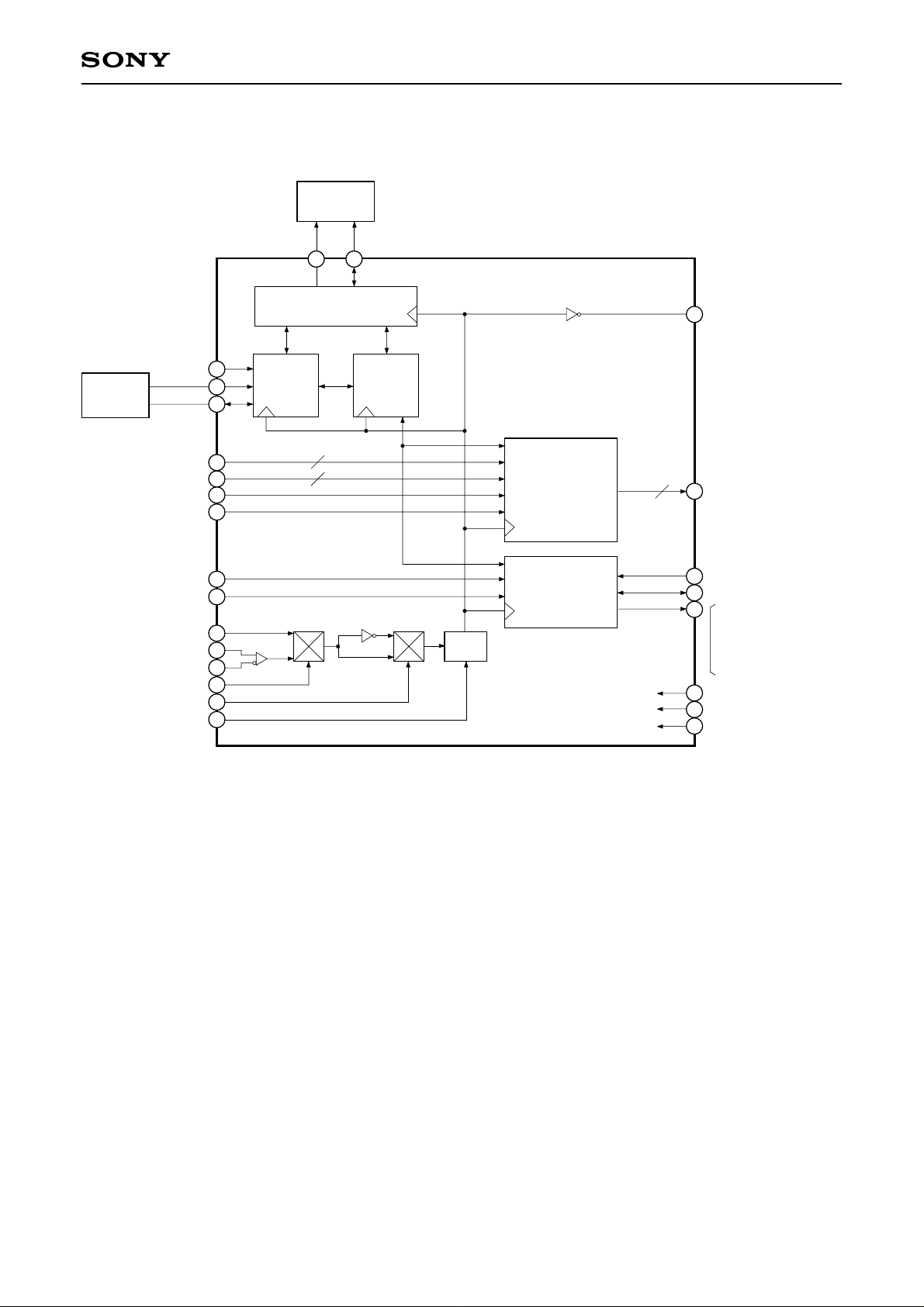
Block Diagram
CXD3526GG
EEPROM
Host
Controller
HSEL
HSCL
HSDA
R, G, BIN
R, G, BOSD
YM
YS
HDIN
VDIN
CLKC
CLKP
CLKN
CLKSEL
CLKPOL
PLLDIV
RSCL
External ROM I/F
Host I/F
10 × 3
2 × 3
RSDA
Register I/F
PLL
DSD
TG
10 × 3
Direct Clear
CLKOUT
R, G, BOUT
CTRL
RGT, DWN
HST, PST, HCK1, HCK2,
DCK1, DCK2, ENB, PCG,
PRG, SHST, HD2, HD3,
CLR, CLP, HD1, VST,
VCK, FRP, XFRP, XRGT,
PO1, PO2
XCLR1
XCLR2
XCLR3
– 2 –
Page 3
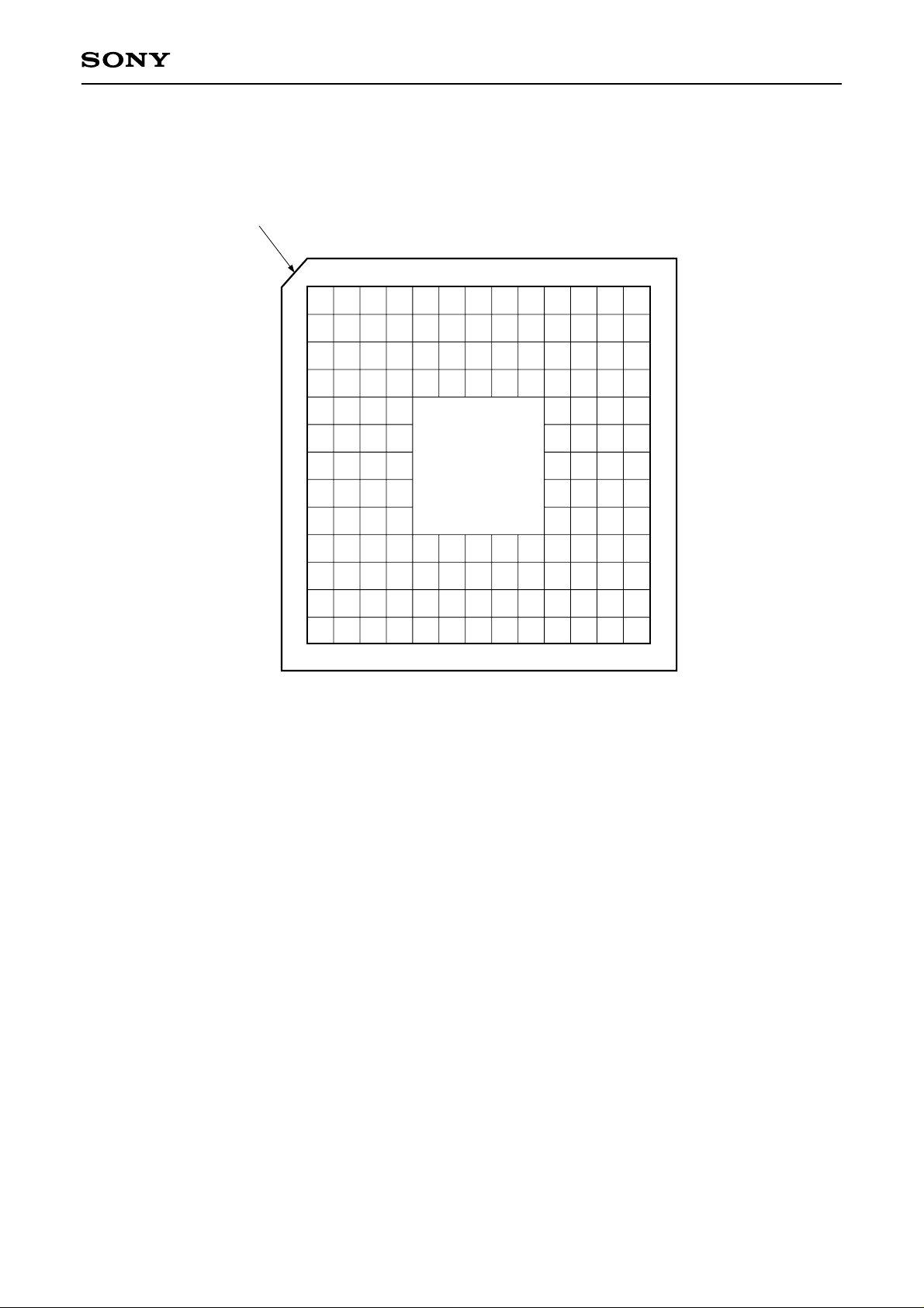
Pin Configuration
CXD3526GG
Index
12345678910111213
A
B
C
D
E
F
G
H
J
K
L
M
N 141516171819202122232425
1 484746454443424140393837
2 498887868584838281807936
3 50 89 120 119 118 117 116 115 114 113 78 35
4 51 90 121 144 143 142 141 140 139 112 77 34
5 52 91 122 138 111 76 33
6 53 92 123 137 110 75 32
7 54 93 124 136(T op Vie w) 109 74 31
8 55 94 125 135 108 73 30
9 56 95 126 134 107 72 29
10 57 96 127 128 129 130 131 132 133 106 71 28
11 58 97 98 99 100 101 102 103 104 105 70 27
12 59 60 61 62 63 64 65 66 67 68 69 26
13
– 3 –
Page 4
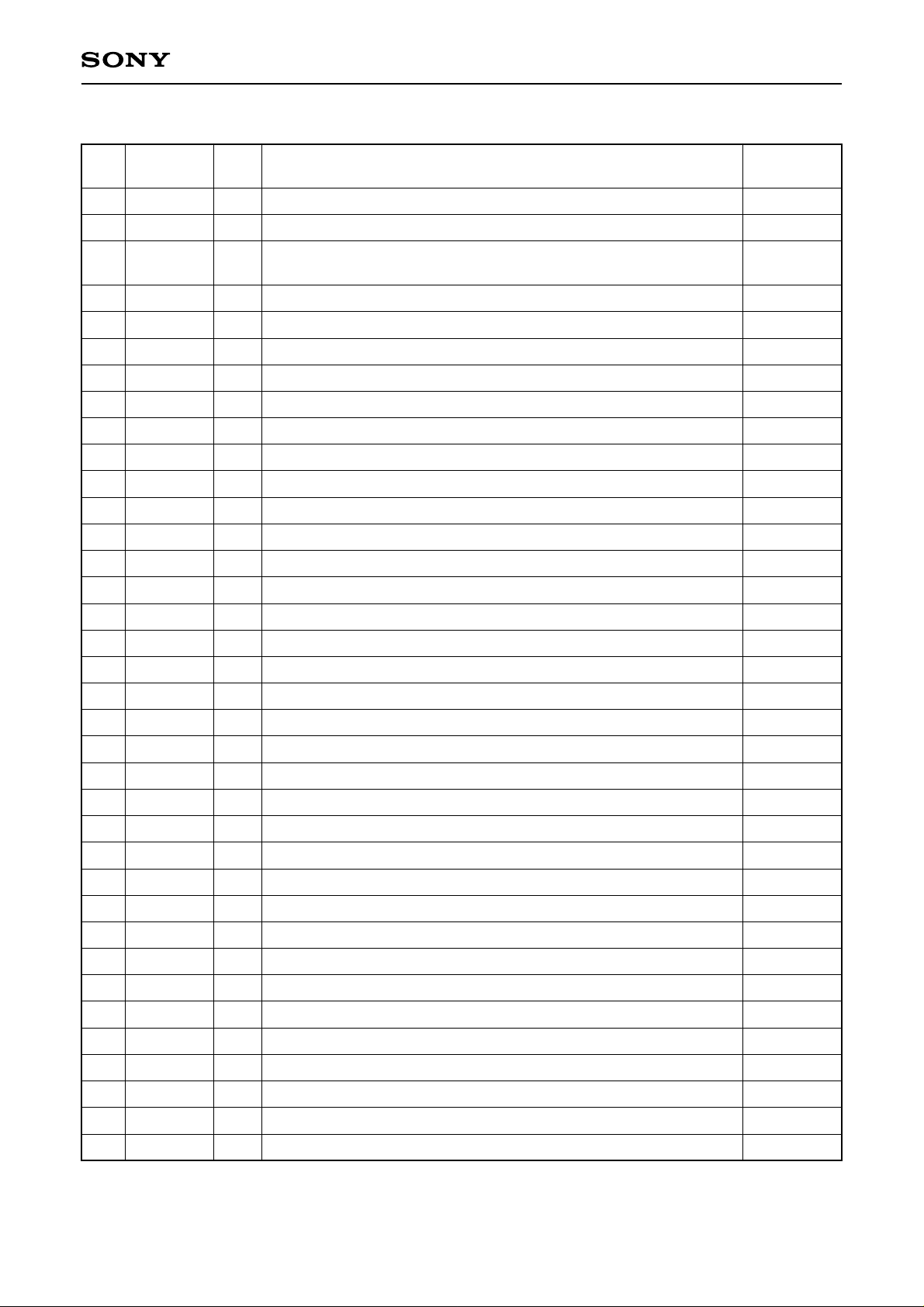
Pin Description
Pin
No.
Symbol
1
VSS
RGT
2
I/O
—
GND
I/O
Horizontal scan direction switching signal I/O
Description
CXD3526GG
Input pin
processing for
open status
—
—
10
11
12
13
14
15
16
17
18
19
3
4
5
6
7
8
9
XRGT
RIN5
RIN2
RIN0
GIN4
GIN0
BIN7
BIN4
BIN1
BIN0
V
SS
ROSD0
GOSD0
BOSD0
VDIN
TEST1
VSS
Horizontal scan direction switching signal output
O
(reversed polarity of RGT)
I
Red data input
I
Red data input
I
Red data input
I
Green data input
I
Green data input
I
Blue data input
I
Blue data input
I
Blue data input
I
Blue data input
—
GND
I
OSD red data input
I
OSD green data input
I
OSD blue data input
I
Vertical sync signal input
—
Test pin (Connect to GND.)
—
GND
—
—
—
—
—
—
—
—
—
—
—
—
—
—
—
—
—
20
21
22
23
24
25
26
27
28
29
30
31
32
33
34
35
36
VDD1
VSS
HSEL
RSCL
TEST2
VSS
TEST3
TEST4
CLKOUT
BOUT3
VDD2
VSS
GOUT3
GOUT6
GOUT9
ROUT2
ROUT6
—
Internal operation power supply
—
GND
I
Serial bus slave address selection signal input
I/O
Serial bus clock I/O (external ROM I/F)
—
Test pin (Connect to VDD2.)
—
GND
—
Test pin (Connect to VDD2.)
—
Test pin (Connect to VDD2.)
O
Internal clock output (inverted output)
O
Blue data output
—
I/O power supply
—
GND
O
Green data output
O
Green data output
O
Green data output
O
Red data output
O
Red data output
—
—
—
—
—
—
—
—
—
—
—
—
—
—
—
—
—
– 4 –
Page 5
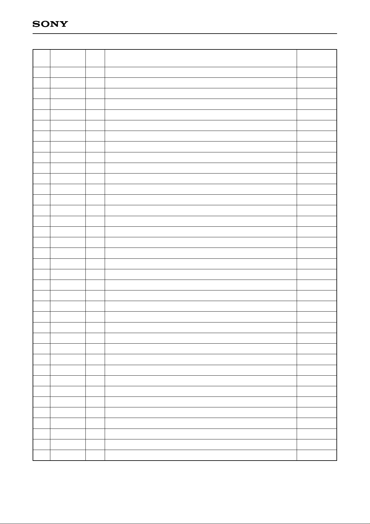
CXD3526GG
Pin
No.
37
38
39
40
41
42
43
44
45
46
47
48
49
50
51
52
Symbol
VSS
ROUT9
ROUT8
ROUT7
VST
HD2
HD3
VDD2
PRG
ENB
PO1
PO2
DWN
RIN8
RIN6
RIN3
I/O
—
GND
O
Red data output
O
Red data output
O
Red data output
O
Vertical display start timing pulse output
O
Horizontal auxiliary pulse output 2
O
Horizontal auxiliary pulse output 3
—
I/O power supply
O
2-step precharge timing pulse output
O
Gate enable pulse output
O
Parallel output 1
O
Parallel output 2
I/O
Vertical scan direction switching signal I/O
I
Red data input
I
Red data input
I
Red data input
Description
Input pin
processing for
open status
—
—
—
—
—
—
—
—
—
—
—
—
—
—
—
—
53
54
55
56
57
58
59
60
61
62
63
64
65
66
67
68
69
RIN1
GIN5
GIN1
BIN8
BIN5
BIN2
ROSD1
GOSD1
BOSD1
HDIN
CLKPOL
VSS
TEST5
XCLR2
TEST6
HSCL
RSDA
I
Red data input
I
Green data input
I
Green data input
I
Blue data input
I
Blue data input
I
Blue data input
I
OSD red data input
I
OSD green data input
I
OSD blue data input
I
Horizontal sync signal input
I
Internal clock polarity selection (High: inverted; Low: non-inverted)
—
GND
—
Test pin (Connect to VDD2.)
I
External clear (Low: reset)
—
Test pin (Connect to GND.)
I
Serial bus clock (host I/F)
I/O
Serial bus data I/O (external ROM I/F)
—
—
—
—
—
—
—
—
—
—
L
—
—
H
—
—
—
70
71
72
73
HSDA
VSS
BOUT2
BOUT6
I/O
Serial bus data I/O (host I/F)
—
GND
O
Blue data output
O
Blue data output
—
—
—
—
– 5 –
Page 6
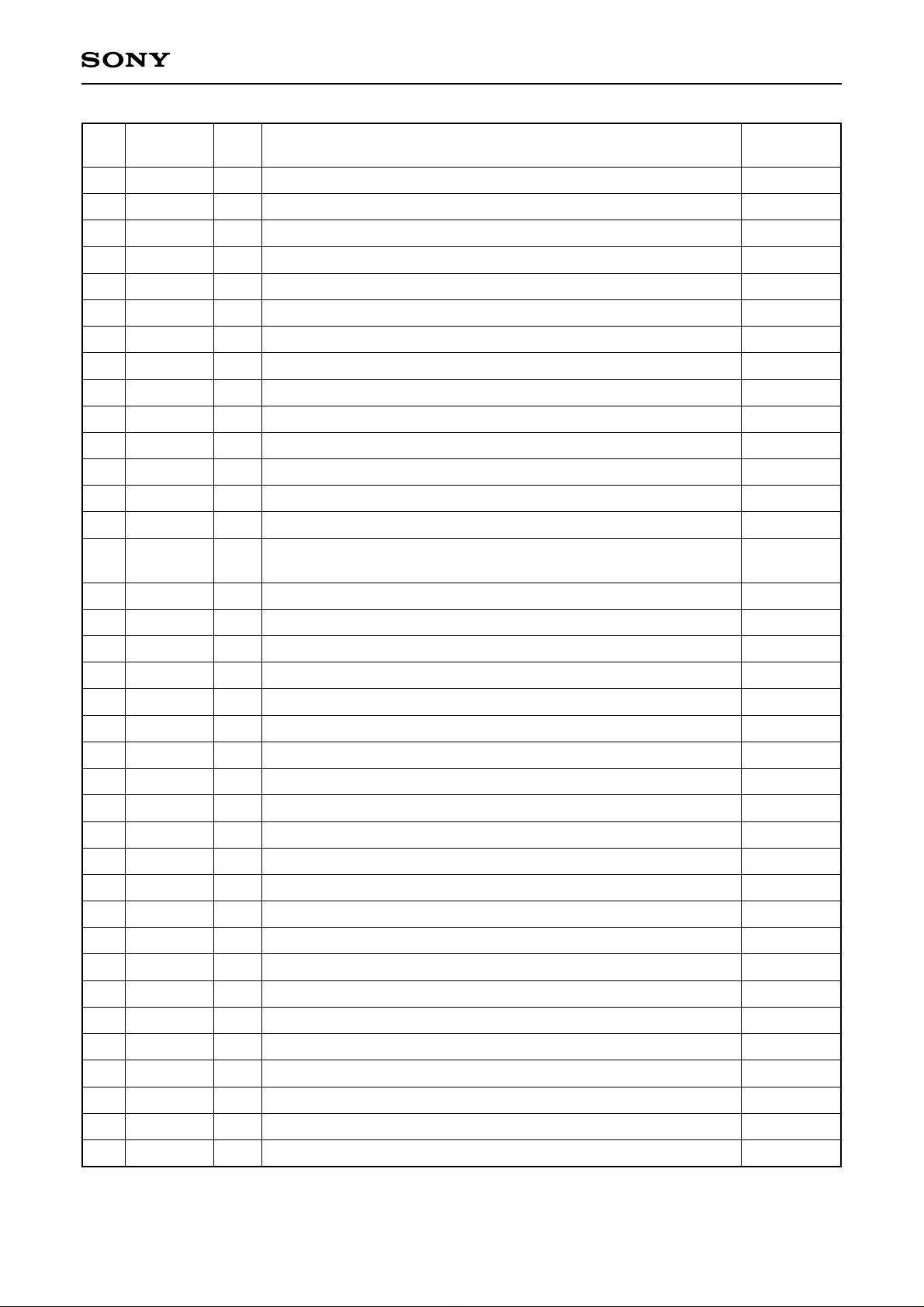
CXD3526GG
Pin
No.
74
75
76
77
78
79
80
81
82
83
84
85
86
87
88
Symbol
BOUT9
GOUT2
GOUT5
GOUT8
ROUT1
ROUT5
ROUT4
ROUT3
VCK
HD1
PCG
VSS
CLR
DCK1
CTRL
I/O
O
Blue data output
O
Green data output
O
Green data output
O
Green data output
O
Red data output
O
Red data output
O
Red data output
O
Red data output
O
Vertical display transfer clock output
O
Horizontal auxiliary pulse output 1
O
Collective precharge timing pulse output
—
GND
O
CLR pulse output
O
DCK1 pulse output
Scan direction control method switching
I
(Low: internal register ; High: external)
Description
Input pin
processing for
open status
—
—
—
—
—
—
—
—
—
—
—
—
—
—
L
89
90
91
92
93
94
95
96
97
98
99
100
101
102
103
104
105
RIN9
RIN7
RIN4
GIN8
GIN6
GIN2
BIN9
BIN6
BIN3
YM
YS
CLKSEL
CLKP
XCLR1
XCLR3
TEST7
VSS
I
Red data input
I
Red data input
I
Red data input
I
Green data input
I
Green data input
I
Green data input
I
Blue data input
I
Blue data input
I
Blue data input
I
OSD YM input
I
OSD YS input
I
Input clock selection (High: CLKC; Low: CLKP/N)
I
Clock input (small-amplitude differential input, positive polarity)
I
External clear (Low: reset)
I
External clear (Low: reset)
—
Test pin (Connect to GND.)
—
GND
—
—
—
—
—
—
—
—
—
L
L
L
—
H
H
—
—
106
107
108
109
110
BOUT0
BOUT1
BOUT5
BOUT8
GOUT1
O
Blue data output
O
Blue data output
O
Blue data output
O
Blue data output
O
Green data output
—
—
—
—
—
– 6 –
Page 7
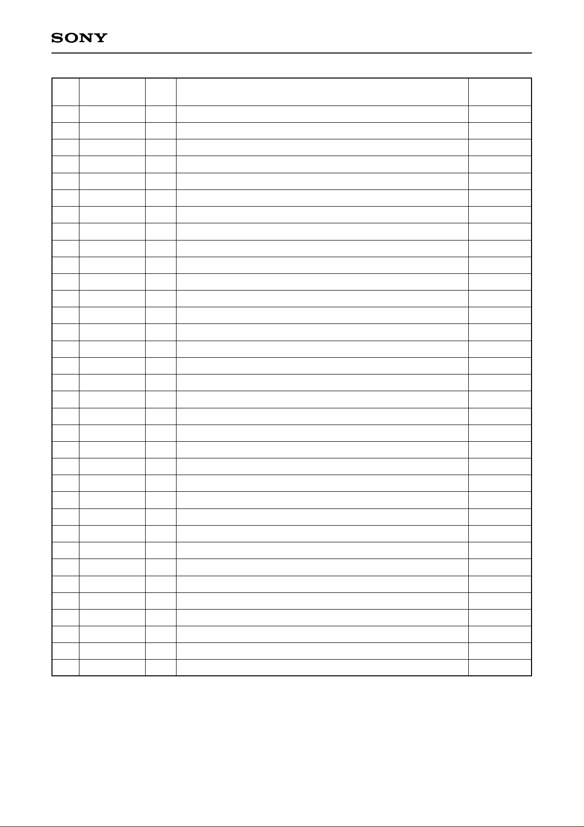
CXD3526GG
Pin
No.
111
112
113
114
115
116
117
118
119
120
121
122
123
124
125
126
Symbol
GOUT4
GOUT7
ROUT0
VDD2
CLP
HST
HCK1
FRP
SHST
DCK2
VSS
VDD1
GIN9
GIN7
GIN3
VDD2
I/O
O
Green data output
O
Green data output
O
Red data input
—
I/O power supply
O
CLP pulse output
O
Horizontal display start timing pulse output
O
Horizontal display transfer clock output 1
O
AC drive inversion timing pulse output
O
SHST pulse output
O
DCK2 pulse output
—
GND
—
Internal operation power supply
I
Green data input
I
Green data input
I
Green data input
—
I/O power supply
Description
Input pin
processing for
open status
—
—
—
—
—
—
—
—
—
—
—
—
—
—
—
—
127
128
129
130
131
132
133
134
135
136
137
138
139
140
141
142
143
Vss
VDD1
PLLDIV
CLKN
CLKC
VDD2
VSS
VDD1
BOUT4
BOUT7
GOUT0
VDD2
VSS
VDD1
PST
HCK2
XFRP
—
GND
—
Internal operation power supply
I
Internal PLL setting (High: 55MHz or less; Low: 55MHz or more)
I
Clock input (small-amplitude differential input, negative polarity)
I
Clock input (CMOS input)
—
I/O power supply
—
GND
—
Internal operation power supply
O
Blue data output
O
Blue data output
O
Green data output
—
I/O power supply
—
GND
—
Internal operation power supply
O
Dot sequential precharge start timing pulse output
O
Horizontal display transfer clock output 2
O
AC drive inversion timing pulse output (reversed polar ity of FRP)
—
—
L
—
—
—
—
—
—
—
—
—
—
—
—
—
—
144
VDD2
—
I/O power supply
—
– 7 –
Page 8
CXD3526GG
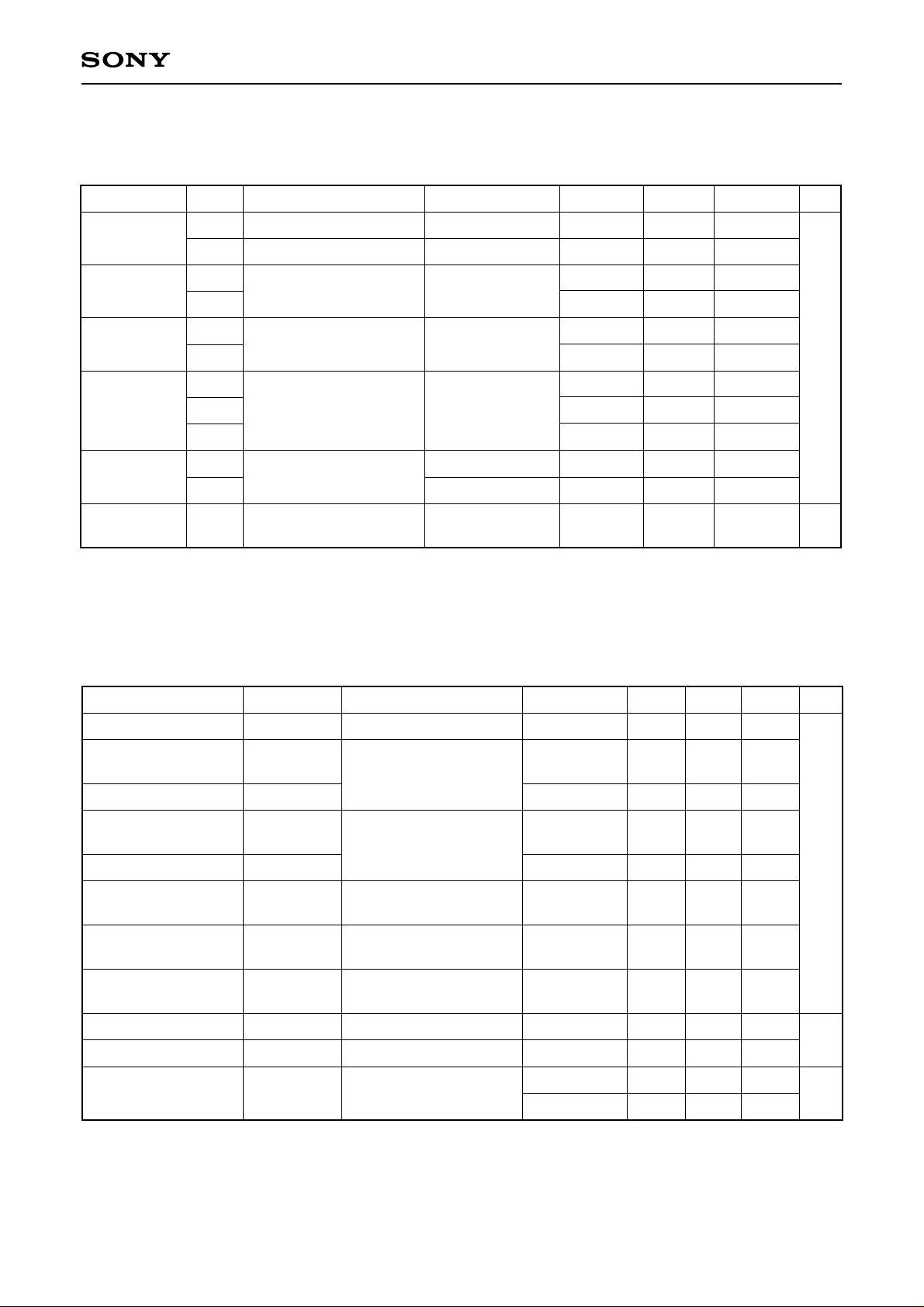
Electrical Characteristics
DC Characteristics (Topr = –20 to +75°C, VSS = 0V)
Item Symbol Applicable pins Conditions Min. Typ. Max.
Supply
voltage
Input
voltage 1
Input
voltage 2
Input
voltage 3
VDD1
VDD2
VIH1
VIL1
VIH2
VIL2
VC
VIH3
1
∗
HDIN, VDIN, HSCL
2
∗
CLKP, CLKN
VIL3
Output
voltage
Power
consumption
1
∗
Input pins other than those indicated in items Input voltage 2 and Input voltage 3.
2
∗
VIH3 > VC (max.) and VIL3 < VC (min.).
3
∗
Tj [°C] ≥ Toprmax [°C] + θja [°C/W] × PD [W].
VOH
VOL
PD
All output pins
3
∗
—
—
—
—
—
CMOS input cell
CMOS Schmitt
trigger input cell
Small-amplitude
differential input
—
—
CLKP = 85MHz
2.3
3.0
2.0
–0.3
0.8VDD2
–0.3
1.718
1.868
VSS
VDD2 – 0.2
VSS
—
2.5
3.3
—
—
—
—
2.0
VC + 0.4
VC – 0.4
—
—
950
2.7
3.6
DD2 + 0.3
V
0.8
V
DD2 + 0.3
0.2VDD2
2.281
VDD2
2.131
VDD2
0.2
1140
Unit
V
mW
AC Characteristics (Topr = –20 to +75°C, V DD1 = 2.5 ± 0.2V, VDD2 = 3.3 ± 0.3V, VSS = 0V)
Item Symbol Applicable pins Conditions Min. Typ. Max. Unit
Clock input period
Input setup time
—
tis
CLKP, CLKN, CLKC
RGB input, OSD input,
—
—
10.0
2.0
—
—
—
—
HDIN, VDIN
Input hold time
Input setup time
tih
tis
—
—
2.0
5.0
—
—
—
—
HSCL, HSDA, RSDA
Input hold time
Output rise/fall
delay time
Output rise/fall
delay time
Cross-point time
difference
HCK1 duty
tih
tor/tof
tor/tof
∆t
th/(th + tl)
4
∗
FRP, XFRP, SHST,
CLKOUT
HCK1, HCK2, DCK1,
DCK2
HCK1
—
CL = 20pF
CL = 50pF
CL = 20pF
CL = 20pF
5.0
2.5
2.5
–5.0
48
—
4.0
4.0
—
50
—
7.0
7.0
5.0
52
ns
%
HCK2 duty
Phase compensation
PLL operating
frequency
tl/(th + tl)
—
HCK2
—
CL = 20pF
PLLDIV = L
PLLDIV = H
48
55
27.5
50
—
—
52
100
MHz
55
4
∗
Output pins other than FRP, XFRP, SHST and CLKOUT.
– 8 –
Page 9
CXD3526GG
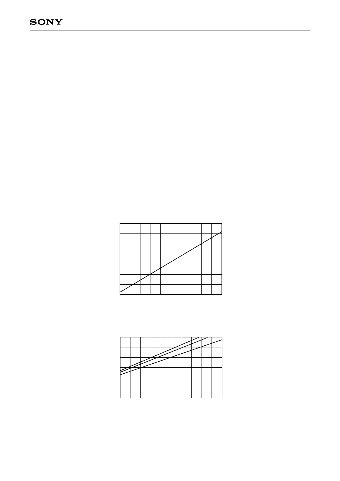
Power Consumption and Allowable Power Dissipation
The relationship between the power consumption and junction temperature of this IC must satisfy the following
formula.
Tj [°C] ≥ Toprmax [°C] + θja [°C/W] × PD [W]
In addition, specification values are as follows.
Tjmax = 125 [°C]
Toprmax = 75 [°C]
θja = 43 [°C/W] (When mounted on 4-layer substrate, wind speed 0m/s)
Under these conditions, PDmax, the maximum allowable power dissipation for the package, is as follows.
PDmax = (125 – 75)/43 = 1162 [mW]
Further more, if the operating frequency of this IC exceeds 85MHz, the junction temperature may exceed its
maximum value depending on conditions of use. Use this IC under conditions where the maximum value for
the junction temperature will not be exceeded by lowering the thermal resistance of the package as follows by
taking thermal countermeasures at this time.
Wind speed 1m/s: θja = 40 [°C/W] (When mounted on 4-layer substrate)
Wind speed 3m/s: θja = 35 [°C/W] (When mounted on 4-layer substrate)
1400
1300
1200
1100
1000
900
Power consumption [mW]
800
700
50
60 70
Operating frequency [MHz]
80 90 100
Operating Frequency vs. Power Consumption (Maximum Values)
130
120
110
43˚C/W
40˚C/W
35˚C/W
100
90
80
Junction temperature [˚C]
70
500
700 900
Power consumption [mW]
1100 1300 1500
Power Consumption vs. Junction Temperature (for Various Values of Thermal Resistance)
– 9 –
Page 10
CXD3526GG
Power-on and Initialization of Internal Circuit
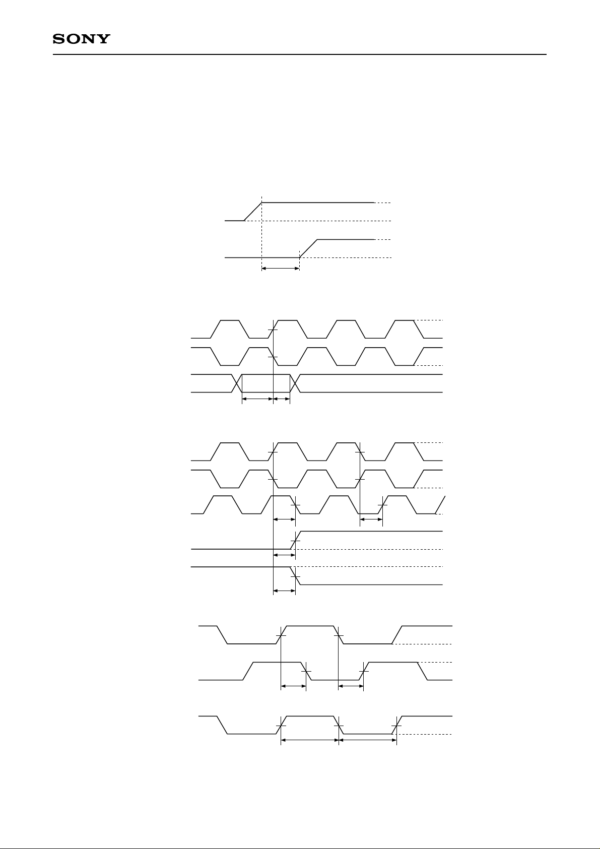
As for this IC, two systems of supply voltage should be turned on simultaneously. The initialization of the
internal circuit should be also performed by maintaining the system clear pin at low during the specified time
after setting the supply voltage in the range of recommended operating conditions and stabilizing as shown in
the figure below. Keep in mind that the internal circuit may not be initialized correctly if system clear
cancellation is performed before the supply voltage is set in the range of the recommended operating
conditions.
Timing Definition
HDIN, VDIN
RGB input, OSD input
XCLR1, XCLR2,
XCLR3
CLKP, CLKC
CLKN
CLKP, CLKC
CLKN
CLKOUT
Outputs other
than CLKOUT
Outputs other
than CLKOUT
V
DD1, VDD2
TR TR > 200ns
VC,
50%
VC
tis tih
VC,
50%
VC
VC
50%
50%
tof
tor
tof
VC,
50%
VC
VC
VDD1, VDD2
Vss
VDD2
Vss
tor
IH1, VIH3
V
V
IL1, VIL3
VIH3
VIL3
VIH1, VIH2
VIL1, VIL2
V
IH1, VIH3
V
SS, VIL3
VIH3
VIL3
VOH
VOL
VOH
VOL
VOH
VOL
HCK1, DCK1
HCK2, DCK2
HCK1, HCK2
50%50%
50%
∆t
50%
th tl
– 10 –
50%
VOH
VOL
VOH
∆t
50%50%
VOL
VOH
VOL
Page 11

CXD3526GG
Description of Operation
1. Description of I/O Pins
(a) System clear pins (XCLR1, XCLR2 and XCLR3)
All internal circuits are initialized by setting XCLR1 (Pin 102) low. In addition, the internal PLL is initialized by
setting XCLR2 (Pin 66) low, and RGB output is initialized (preset) by setting XCLR3 (Pin 103) low.
Initialization should be performed when power is turned on.
(b) Sync signal input pins (HDIN and VDIN)
Horizontal and vertical separate sync signals are input to HDIN (Pin 62) and VDIN (Pin 17), respectively. The
CXD3526GG supports only non-interlace sync signals with a dot clock of 100MHz or less.
(c) Master clock input pins (CLKP/CLKN, CLKC, CLKSEL and CLKPOL)
Phase comparison is performed by an external circuit and a clock synchronized to the sync signal is input. The
master clock input pins have two systems consisting of CLKP/CLKN (Pins 101 and 130) for small-amplitude
differential input (center level: 2.0V, amplitude: ±0.4V), and CLKC (Pin 131) for CMOS level input. In addition,
the clock path selection is performed with CLKSEL (Pin 100) and CLKPOL (Pin 63). The setting values are as
follows.
CLKSEL: 0 = CLKP and CLKN input; 1 = CLKC input
CLKPOL: 0 = Input clock is non-inverted; 1 = Input clock is inverted
(d) PLL setting pin (PLLDIV)
PLLDIV (Pin 129) sets the divider setting of the internal phase compensation PLL circuit. The setting values for
master clock frequency are as follows.
PLLDIV: 0 = 55 to 100MHz; 1 = 27.5 to 55MHz
Note that the frequency of the clock input to the CXD3526GG must be within the phase compensation PLL
operating range, even during free running.
(e) RGB signal input pins (RIN, GIN and BIN)
These pins input RGB digital signals in 10 bits. The Red signal is input to RIN (Pins 4 to 6, 50 to 53 and 89 to
91), the Green signal to GIN (Pins 7, 8, 54, 55, 92, 93 and 123 to 125), and the Blue signal to BIN (Pins 9 to
12, 56 to 58 and 95 to 97) respectively.
(f) OSD signal input pins (ROSD, GOSD, BOSD, YS and Y M)
These pins input OSD signals. The Red signal is input to ROSD (Pins 14 and 59), the Green signal to GOSD
(Pins 15 and 60), and the Blue signal to BOSD (Pins 16 and 61) respectively. In addition, the YM signal is input
to YM (Pin 98), and the YS signal to YS (Pin 99).
– 11 –
Page 12

CXD3526GG
(g) Host I/F serial clock input pin (HSCL)
HSCL (Pin 68) is the clock input pin used to set the I/O timing for serial data from the host. Data is taken from
the HSDA pin when the clock signal rises, and data is output to the HSDA pin when the clock signal falls.
(h) Host I/F serial I/O pin (HSDA)
This is the I/O pin for serial data from the host. It is necessar y to switch the input to the HSDA (Pin 70) while
the signal level of HSCL is low.
(i) Slave address input pin (HSEL)
With this IC, it is possible to select host I/F slave address. Since a slave address is used to identify each of
these devices, this pin should be connected to VDD or Vss externally. This VDD and Vss setting drives the device
which matches the slave address input from the HSDA pin. The slave addresses of this IC used for the HSEL
(Pin 22) setting are as follows.
HSEL: 0 = 74h; 1 = 76h
(j) External ROM I/F serial clock output pin (RSCL)
RSCL (Pin 23) is the clock output pin used to set the I/O timing of serial data sent to the external EEPROM.
Data is taken from the RSDA pin when the clock signal r ises, and data is output to the RSDA pin when the
clock signal falls.
(k) External ROM I/F serial I/O pin (RSDA)
This is the I/O pin for serial data sent to the external EEPROM. It is necessary to switch the input to the RSDA
(Pin 69) while the signal level of RSCL is low.
2. Pipeline Delay of the RGB and OSD Signals
The pipeline delay f or the I/O of the RGB signals is 32 clock cycles of the master clock. In addition, the pipeline
delay for the OSD, YS and YM signals is 25 clock cycles of the master clock.
– 12 –
Page 13
CXD3526GG
3. Serial Bus
The serial bus of this IC consists of a host I/F, external ROM I/F and register I/F.
3-1. Host I/F
With this IC, each register setting and data set to built-in RAM are perfor med over a serial bus. Bus protocol
conforms to I2C bus specifications. Note that this IC does not suppor t multi-slave functions, and that the bus
should be independent from ICs having the other I2C bus specification. Also, when accessing gamma RAM,
always access memory address from odd addresses in 2-byte units. The following restrictions are placed on
the host I/F of this IC.
• Only I2C bus slave operations are performed.
• Standard mode and fast mode are supported. Hs mode is not supported.
• Multi-slave functions are not supported.
• The general call address and start byte of the slave address are not acknowledged.
• C bus compatibility is not supported.
• Acknowledgment is not performed for 10-bit slave addresses.
• Low is not asserted for HSCL. (Wait control is not performed.)
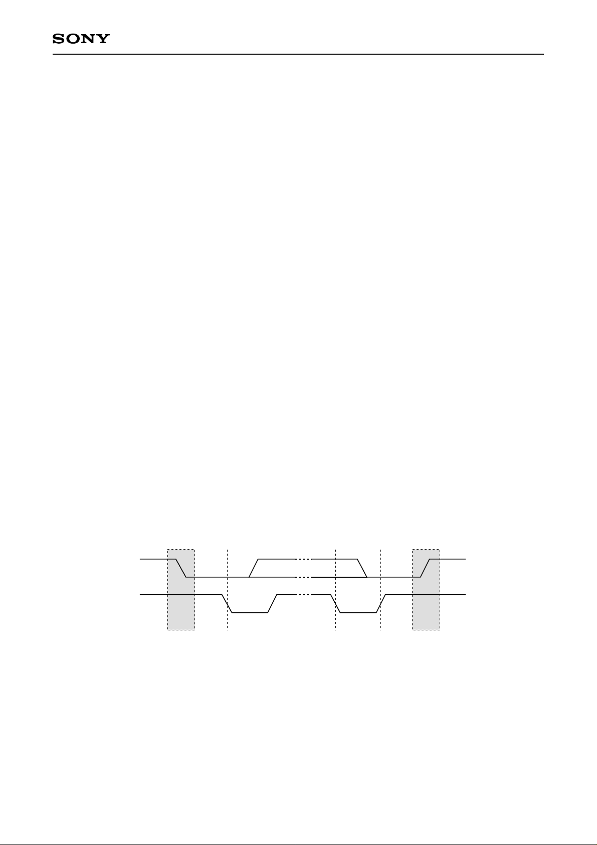
(1) "Start" conditions
Read and write operations enter "Start" status by switching HSDA input from high to low level while HSCL input
is high.
(2) "Stop" conditions
"Stop" results by switching HSDA input from low to high while HSCL input is high. Setting "Stop" status causes
read processing to terminate during read operations, and causes the input of write data to terminate dur ing
write operations.
HSDA
HSCL
"Start" "Stop"
"Start" Conditions and "Stop" Conditions
– 13 –
Page 14
CXD3526GG
(3) Acknowledgment
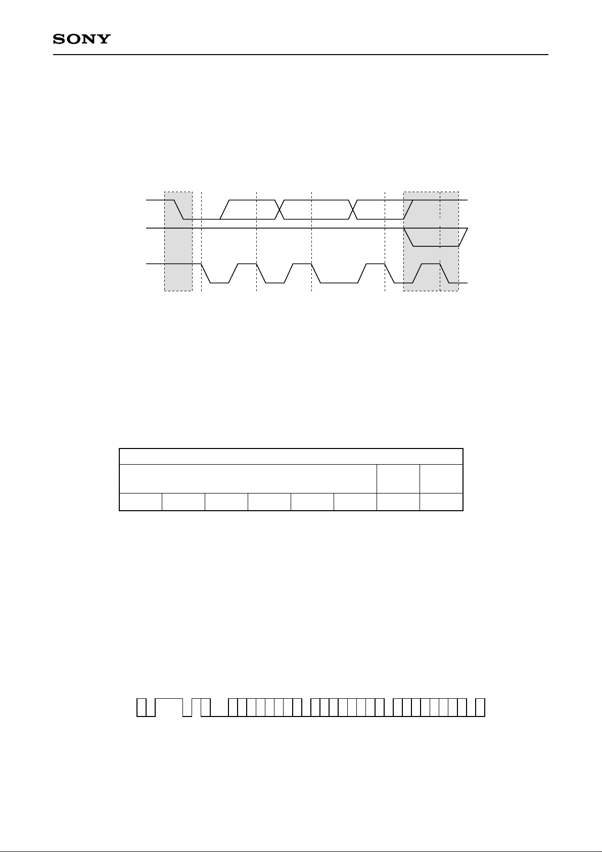
Acknowledgment is used to indicate whether or not data has been sent/received normally. The
"Acknowledgment" of a data transfer is performed after that data transfer when the sender releases the bus on
the 9th clock of HSCL and the receiver drives low. If the host is the receiver, the IC is informed by the host that
data has ended by the fact that "Acknowledgment" is not generated for the last data sent from the IC.
HSDA in
HSDA out
HSCL
12 89
Not
acknowledged
Acknowledged
"
Acknowledgment
""Start"
Acknowledgment on the I2C Bus
(4) Slave address specification
After "Start" is sent, a 7-bit slave address and 1-bit read/write code is sent. Read/write operations with this IC
start if the input slave address matches the device address set using HSEL. If the device address does not
match, "Acknowledgment" is not generated and the system does nothing.
Slave Address Word (8 bits)
Device Code (fixed)
Device
Select
R/W
Code
011101HSEL R/W
∗
If R/W = 1, read results, if R/W = 0, write results.
Slave Address Specification
(5) Byte write operation
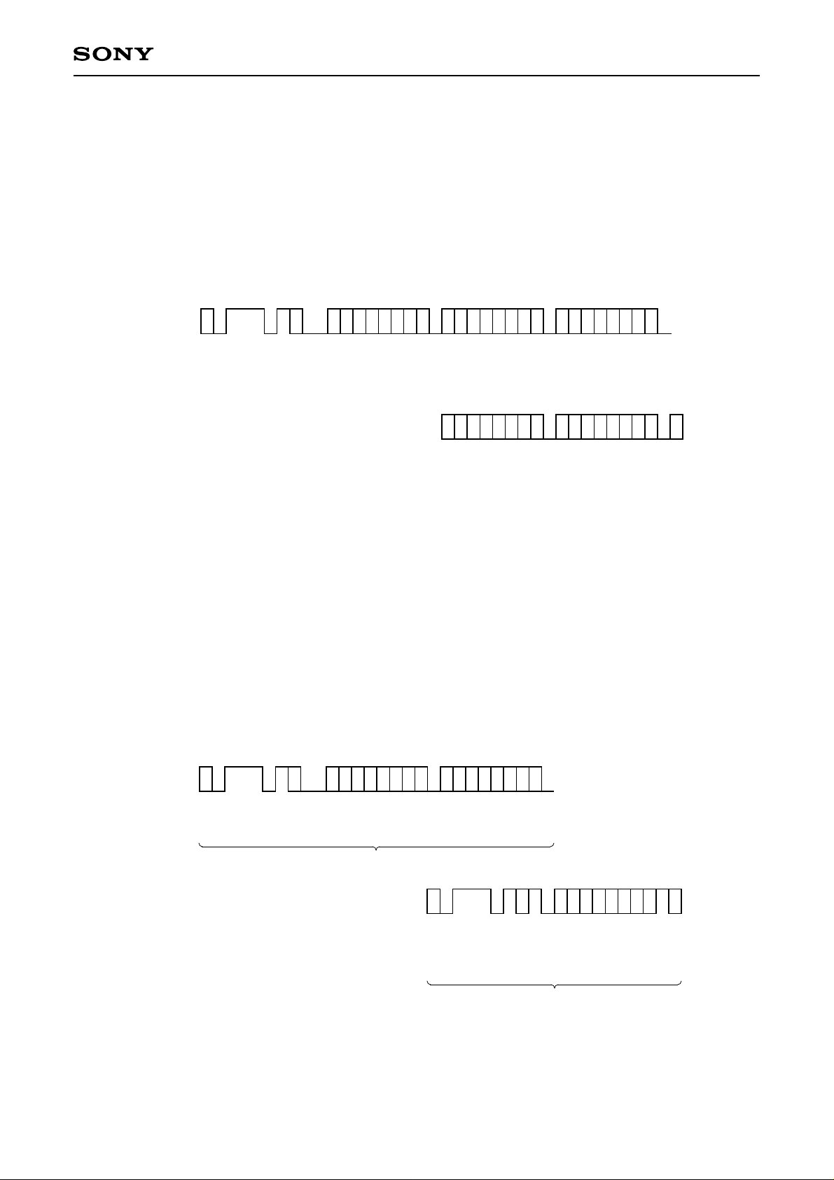
After "Start" is sent, the R/W code is set to low and an 8-bit device address word is input. The IC outputs
"Acknowledgment" on the 9th bit and enters write mode. After this, "Acknowledgment" is output every 8 bits
after each of the two 8-bit memory addresses are input. Next, "Acknowledgment" is output after 8 bits of write
data is input and written to the IC.
HSDA
1st memory address
1W01110
R/W
ACK
START
HSEL
A15
A14
A13
(n)
A12
A11
2nd memory address
A9A8A7A6A5A4A3A2A1
A10
ACK
(n) Write data (n)Slave address
A0
D7D6D5D4D3D2D1
ACK
D0
ACK
STOP
Byte Write Operation
– 14 –
Page 15
CXD3526GG
(6) Continuous write operation
This IC possesses a function which can write data continuously. With the continuous write operation, write data
is written in a manner similar to the byte write operation. Continuous write is possible by sending write data
continuously before sending "Stop". The address used to write data during the continuous write operation is
automatically incremented when each separate write operation terminates.
There is no limit on the number of continuous transfers that are possible to write continuously with this IC.
HSDA
1st memory address
1W01110
R/W
ACK
START
HSEL
A15
(n)
A14
A13
• • • • • • • •
A12
A11
2nd memory address
A9A8A7A6A5A4A3A2A1
A10
ACK
(n) Write data (n)Slave address
D7D6D5D4D3D2D1D0D7D6D5D4D3D2D1
A0
D7D6D5D4D3D2D1
ACK
Write data (n + m)
ACK
D0
D0
ACK
ACK
STOP
Continuous Write Operation
(7) Byte read operation
After "Start" is sent, the R/W code is set to low and an 8-bit device address word is input. The IC outputs
"Acknowledgment" to the 9th bit and enters write mode. After this, "Acknowledgment" is output ever y 8 bits
after each of the two 8-bit memory addresses are input. Once the addresses are acknowledgment, "Restart" is
input, and the R/W code is set to high, an 8-bit device address word is input, and the IC outputs
"Acknowledgment" to the 9th bit and enters read mode. Next, 8 bits of read data are output using the address
used for the dummy write, and the read operation terminates if "Stop" is input without inputting
"Acknowledgment".
HSDA
1st memory address
1W01110
R/W
ACK
START
HSEL
(n)
A15
A14
A13
A12
Dummy write
A11
2nd memory address
A9A8A7A6A5A4A3A2A1
A10
ACK
Slave address Read data (n)
RESTART
(n)Slave address
A0
ACK
1R01110
Current address read
D7D6D5D4D3D2D1
R/W
ACK
HSEL
D0
STOP
No ACK
Byte Read Operation
– 15 –
Page 16
CXD3526GG
(8) Continuous read operation
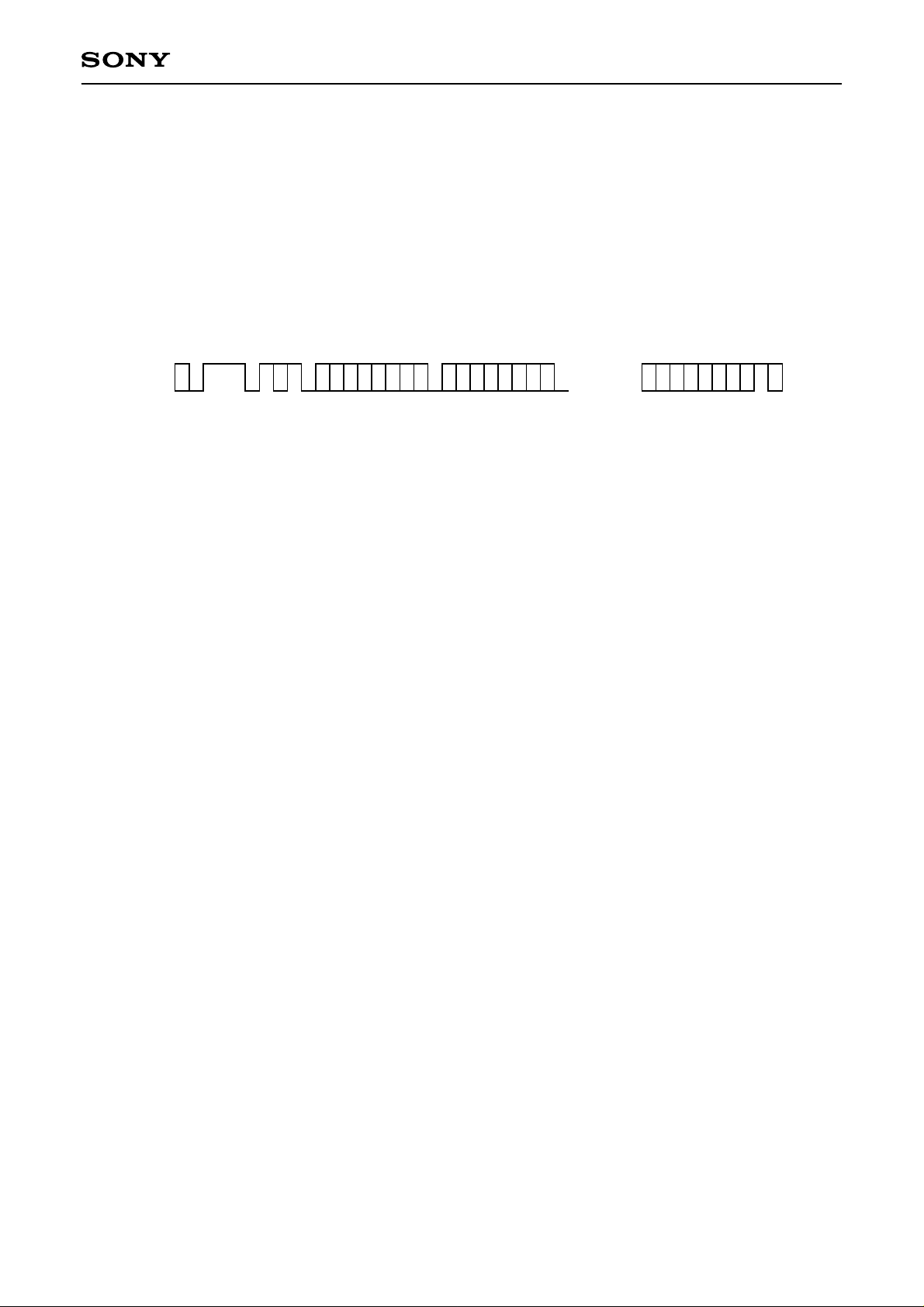
This IC possesses a function which can read data continuously. With the continuous read operation, data up to
the current address is read in a manner similar to the byte read operation. Continuous read is possible by
receiving continuous read data and perform "Acknowledgment" before sending "Stop". The address used for
reading data during the continuous read operation is automatically incremented when each separate read
operation terminates.
There is no limit on the number of continuous transfers that are possible to read continuously with this IC.
Slave address Read data (n) Read data (n + 1) Read data (n + m)
1R01110
START
or
RESTART
R/W
HSEL
D7
D6D5D4D3D2D1D0D7D6D5D4D3D2D1D0
ACK
ACK
• • • • • • • •
ACK
D7D6D5D4D3D2D1
D0
STOP
No ACK
Continuous Read Operation
– 16 –
Page 17
CXD3526GG
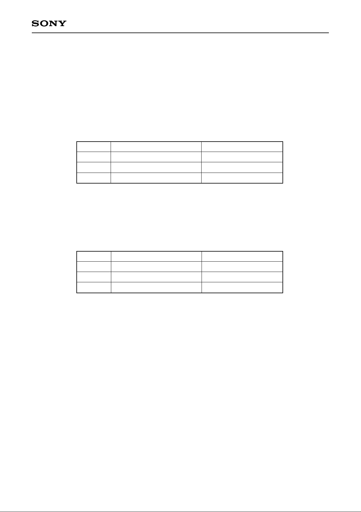
3-2. Conditions for Accessing Gamma RAM and Color Shading RAM
With this IC, there are two way to access the internal RAM: by the host I/F using the serial bus and refresh/
write-back for sending/receiving data via external ROM I/F. In the case of Gamma RAM, internal RAM must be
accessed by the host I/F in 2-byte units, and memory address must be read from or written to odd memory
addresses. Color shading RAM can be accessed in 1-byte units and there is no restriction on which addresses
can be read or written.
It is possible to access internal RAM from each I/F when the conditions given in the following table are
established.
GAM_ON
0
1
1
∗
GAM_ON represents the setting value of the DSD register.
∗
Gamma correction is not performed when GAM_ON is "0", and is performed when
Vertical blanking period
—
Vertical blanking period
Outside vertical blanking period
Gamma RAM access
Yes
Yes
No
GAM_ON is "1".
Conditions for Accessing Gamma RAM
CSC_ON
0
1
1
∗
CSC_ON represents the setting value of the color shading register.
∗
Color shading correction is not performed when CSC_ON is "0", and is performed when
Vertical blanking period
—
Vertical blanking period
Outside vertical blanking period
Color shading RAM access
Yes
Yes
No
CSC_ON is "1".
Conditions for Accessing Color Shading RAM
GAM_ON must be set to "0" when performing a write-back or forced refresh operation for Gamma RAM.
Similarly, CSC_ON must be set to "0" when performing a write-back or forced refresh operation for color
shading RAM.
In the case of a self-refresh operation, the start of vertical blanking period is automatically detected and
operations start automatically at that time, regardless of how GAM_ON and CSC_ON are set. Therefore, be
sure to set the external EEPROM transfer count register ROM_TRAN to fit within the ver tical blanking period.
Furthermore, the vertical blanking period for gamma is set using GAM_H1, GAM_H2, GAM_V1 and GAM_V2,
while the vertical blanking period for color shading is set using CSC_HP, CSC_VP, CSC_HNUM, CSC_VNUM,
CSC_HINT and CSC_VINT. Make all settings in accordance with the specifications of the video signal
attempting to be displayed.
– 17 –
Page 18
CXD3526GG
3-3. External ROM I/F
When operating the external ROM I/F, operations start by setting the serial bus register from the host I/F. The
serial bus on the ROM side is used to access the external EEPROM. Bus protocol conforms to I2C bus
specifications. Also, the following restrictions are placed on the external ROM I/F of this IC.
• Only master operations are performed.
• Standard mode and fast mode are supported. Hs mode is not supported.
• Multi-master functions are not supported.
• The general call address and start byte of the slave address are not generated.
• C bus compatibility is not supported.
• A memory address space of up to 512K bytes is supported.
• Wait control by RSCL is not supported.
• 10-bit slave addresses are not supported.
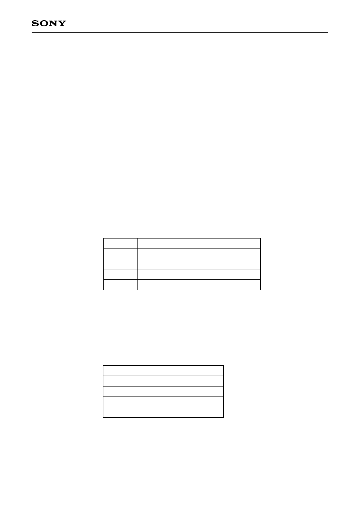
(1) External ROM I/F clock settings
The frequency of the clock signal supplied to the external EEPROM by the RSCL pin is set using RSCL_SEL
of the serial bus control registers. Set this value based on the operating frequency of the IC as given in the
table below so that the frequency output by the RSCL pin is appropriate for the specifications of the external
EEPROM.
RSCL_SEL
00
01
10
11
Operating frequency
35MHz or less
70MHz or less
94.5MHz or less
100MHz or less
(2) External EEPROM memory capacity setting
With this IC, slave addresses and memory addresses are generated in accordance with the memory capacity
set for the external EEPROM. The memory capacity of the external EEPROM is set using ROM_MAP of the
serial bus control registers.
ROM_MAP
Usable memory size
00
01
10
11
512K-bit (65,536 × 8-bit)
256K-bit (32,768 × 8-bit)
128K-bit (16,384 × 8-bit)
64K-bit (8,192 × 8-bit)
– 18 –
Page 19
CXD3526GG
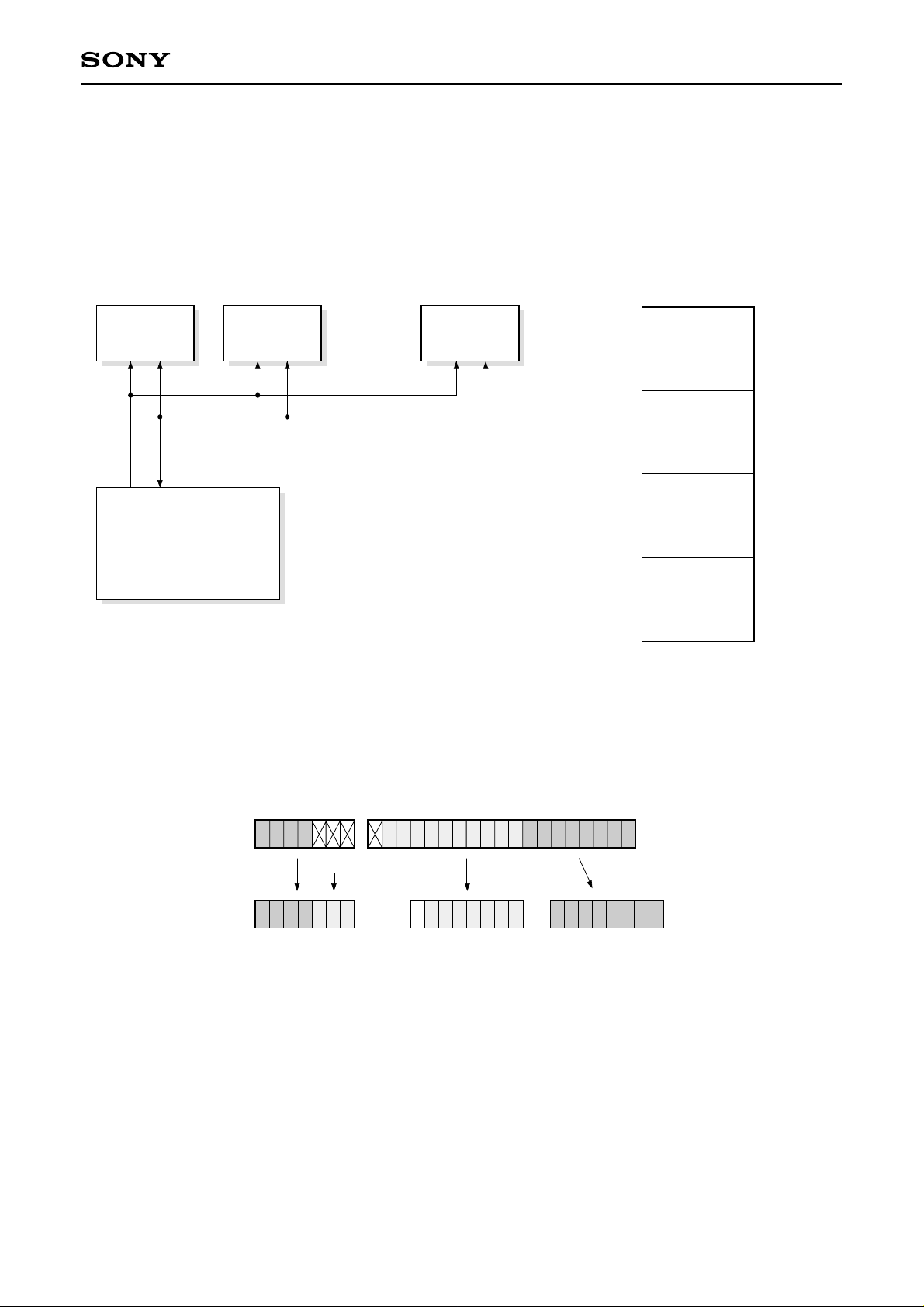
[Example] Address output when using eight 256K-byte EEPROMs (ROM_MAP = 01)
With this IC, the ROM slave address register setting [7:4] is set as is for the serial bus slave address [7:4], and
the memory address [17:15] is used for the slave address [3:1]. The memory address [14:0] is used as is for
the 1st and 2nd memory addresses. The 1st memor y address [7] is fixed to all "0". Furthermore, up to eight
external EEPROMs can be connected to this IC.
Bank 0
RSCL
EEPROM
256K-bit
CXD3526GG
Bank 1
X0h
RSDA
EEPROM
256K-bit
X1h X7h
• • • • • • •
System Configuration Diagram
Bank 7
EEPROM
256K-bit
0_0000h
0_7FFFh
0_8000h
0_FFFFh
1_0000h
3_7FFFh
3_8000h
3_FFFFh
Bank 0
32K-byte
Bank 1
32K-byte
•
•
•
Bank 7
32K-byte
Memory Map
256K-byte space
Slave address
X0h
X1h
X7h
Slave address register [7:4] Memory address [18:0]
74 0118
717
Slave address [7:1]
1st memory address [7:0] 2nd memory address [7:0]
0
0 70
– 19 –
Page 20
CXD3526GG
(3) External ROM I/F slave address setting
The external ROM I/F of this IC transfers data into and out of memory using the serial bus as host I/F. Since
operations conform to I2C bus protocol just as with the host I/F, this section only describes the slave address.
To access the external EEPROM, when access conditions are established, "Start" is sent, and then 7 bits
representing the slave address are output, and the R/W code is output. "Acknowledgment" is received to the
9th bit from the external EEPROM, and the IC enters either read or write mode. The slave address is
determined based on ROM_MAP of the serial bus ROM I/F control register and RSLV_ADDR of the ser ial bus
ROM slave address register as previously described.
The user should set the upper 4 bits of the device address of the EEPR OM to be used in RSLV_ADDR and the
memory size in ROM_MAP. This allows memory to be used without awareness of memory boundaries of
actual memory used for the setting memory space.
RSDA
1st memory address
W
R/W
START
ACK
A15
A14
A13
(n)
A12
A11
2nd memory address
A9A8A7A6A5A4A3A2A1
A10
ACK
(n) Write data (n)Slave address
A0
D7D6D5D4D3D2D1
ACK
D0
ACK
STOP
Byte Write Operation
(4) Memory location and data size setting for the external EEPROM
Since this IC performs refresh and write-back operations, it is necessary to set which addresses of the
external EEPROM gamma data and color shading data have been located in.
The registers used to make these settings are the external EEPROM gamma data start address register and
the external EEPROM color shading data start address register. By specifying the star ting position of the data
area in these registers data access from the specified addresses is possible during refresh or write-back
operation.
Units of 1K-byte can be used to set the start addresses which can be set in these registers.
In addition, the size of data transferred during refresh and write-back operations is fixed at 2K bytes for each
color in the case of gamma data. The n umber of bytes transferred in the case of color shading data is the value
stored in the color shading data size register plus one.
– 20 –
Page 21

CXD3526GG
(5) Refresh and write-back operations
This IC includes a function that allows an external EEPROM to automatically refresh the internal RAM. This
function has the four modes described below.
• Self-refresh mode
• Forced refresh mode
• Write-back mode
• Refresh stop mode
Each mode is started by writing the specified mode into REF_MODE of the refresh register.
In self-refresh mode, the IC detects that the vertical blanking period has been entered and, using the value
specified in the external EEPROM transfer count register, uses the continuous read operation to transfer data
of the size "transfer count plus 1" to the external ROM I/F. The data read using the continuous read transfer is
written into the internal RAM.
When the transfer of the all data for the data size is completed, the access area for the internal RAM is
changed, continuous read transfer is executed indefinitely until self-refresh mode is exited, and refresh
operations are automatically carried out on the internal RAM.
In forced refresh mode, continuous read transfer from the external EEPROM is performed for the RAM area
specified by REF_RSEL of the refresh RAM select register, and the read data is wr itten to the inter nal RAM.
When the transfer of all data for the specified RAM area is completed, REF_END of the refresh status register
set to a flag indicating the operation has ended, and operations stop.
If forced refresh operations are to be performed for the entire internal RAM, first set the refresh RAM select
register to gamma RAM (R) and perform the forced refresh operation. Since the refresh RAM select register is
automatically set to the next RAM area after all data is transferred, refresh for the entire RAM can be
completed by repeating the forced refresh operation five times.
In write-back mode, continuous write transfer is performed from the RAM area specified by REF_RSEL of the
refresh RAM select register to the external EEPROM. When the transfer of all data for the specified RAM area
is completed, REF_END of the refresh status register set to a flag indicating the operation has ended, and
operations stop.
If write-back operations are to be performed for the entire internal RAM, first set the refresh RAM select
register to gamma RAM (R) just as for forced refresh operation, and then perform the write-back operation.
Since the refresh RAM select register is automatically set to the next RAM area after all data is transferred,
write-back for the entire RAM can be completed by repeating the write-back operation five times.
In refresh stop mode, the external ROM I/F does not operate and nothing is output on the serial bus.
(6) Forced reset of the external ROM I/F control circuit
With this IC, forced reset is possible in case a problem occurs with the external ROM I/F and the internal
circuit becomes locked. Forced reset initializes only the external ROM I/F control circuit by writing "1" to
ROM_RST of the refresh register. Normal operations are allowed after initialization is complete.
3-4. Register I/F Control Circuit
The register I/F control circuit transfers data between the host I/F and the external ROM I/F. Register data
other than RAM data is stored here. Since registers have a double buffer configuration, data in the first buffer is
synchronized with the internal VD and reflected in the second buffer, while data in the second buffer is input to
each block. Note, however, that data in the serial bus control register has a single buffer configuration.
– 21 –
Page 22
CXD3526GG
3-5. Software Flow
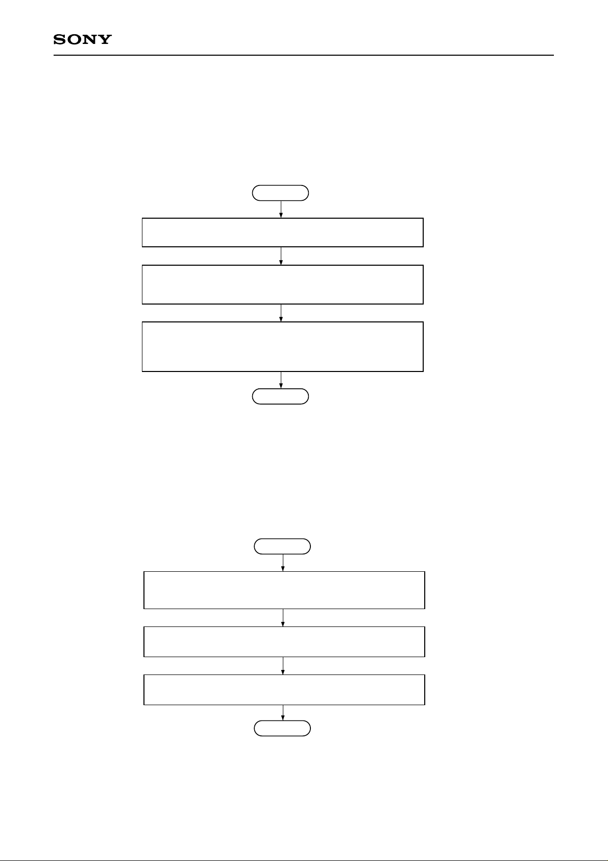
(1) Settings when power is turned on
The following procedure is the setting procedure first perfor med after power of the IC is turned on. If this
procedure is not executed, the internal VD will not be generated and register data cannot be set correctly.
Start
Perform settings such as for the timing of the corresponding LCD panel
using the TG register.
Since the TG register uses a double register configuration using a V latch,
set the FORCE_VD register of the serial bus control register to "1" only at
startup to transfer TG register setting values.
Perform setting for unset registers.
If TG is operating at this time, there is no need to write the FORCE_VD
register due to the fact that registers having a double register configuration
will be automatically written using VD from an external source.
End
(2) Setting procedure of the serial bus control register
The following procedure is the procedure for setting the serial bus control register in accordance with the external
EEPROM to which the IC is connected. Be sure to make settings according to the operating frequency of the IC
and the speed, capacity and number of external EEPROMs that are connected.
Start
Find the optimum clock frequency for the external ROM I/F based on the
frequency of the system clock and set the Bits 1 and 0 of the RSCL_SEL
register to this value.
Set the total capacity of the connected EEPROM devices and set Bits 5
and 4 of the ROM_MAP register to this value.
Set the slave addresses of the EEPROM devices connected into the
RSLV_ADDR register.
End
– 22 –
Page 23
CXD3526GG
(3) Write-back procedure
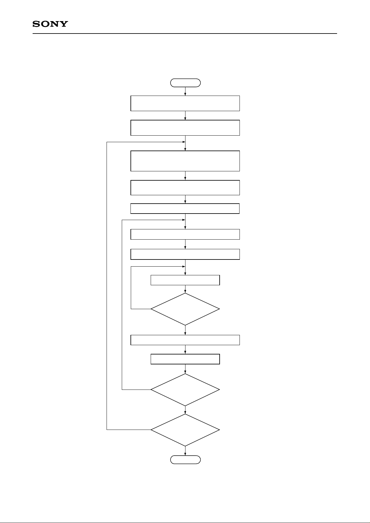
The following procedure is the procedure for writing gamma correction and color shading correction data back
to the external EEPROM.
Start
During display, mute the video signal using the DSD
register.
Set GAM_ON = 0 and CSC_ON = 0 so that the
gamma RAMs and color shading RAMs are not used.
Set the GAM_ADDR, CSC_ADDR, CSC_SIZE and
ROM_TRAN registers to the addresses and transfer
count to be used to perform write-back.
Write data into the gamma RAMs (R, G, B) and color
shading RAMs (R, G, B).
Set the REF_RSEL register to gamma RAM (R).
Write "1" to the REF_END register and clear status.
Write 03h to the REF_MODE register to start write-back.
Read the REF_END register.
Is the status "1"?
0: Write-back currently
being performed
Write "1" to the REF_END register and clear status.
Read the REF_RSEL register.
No
Is write-back complete
for all RAMs?
1: Write-back complete
Write-back other data.
Yes
Is there other gamma
and color shading data
to be written back?
End
End
– 23 –
Page 24
CXD3526GG
(4) Forced refresh procedure during power-on
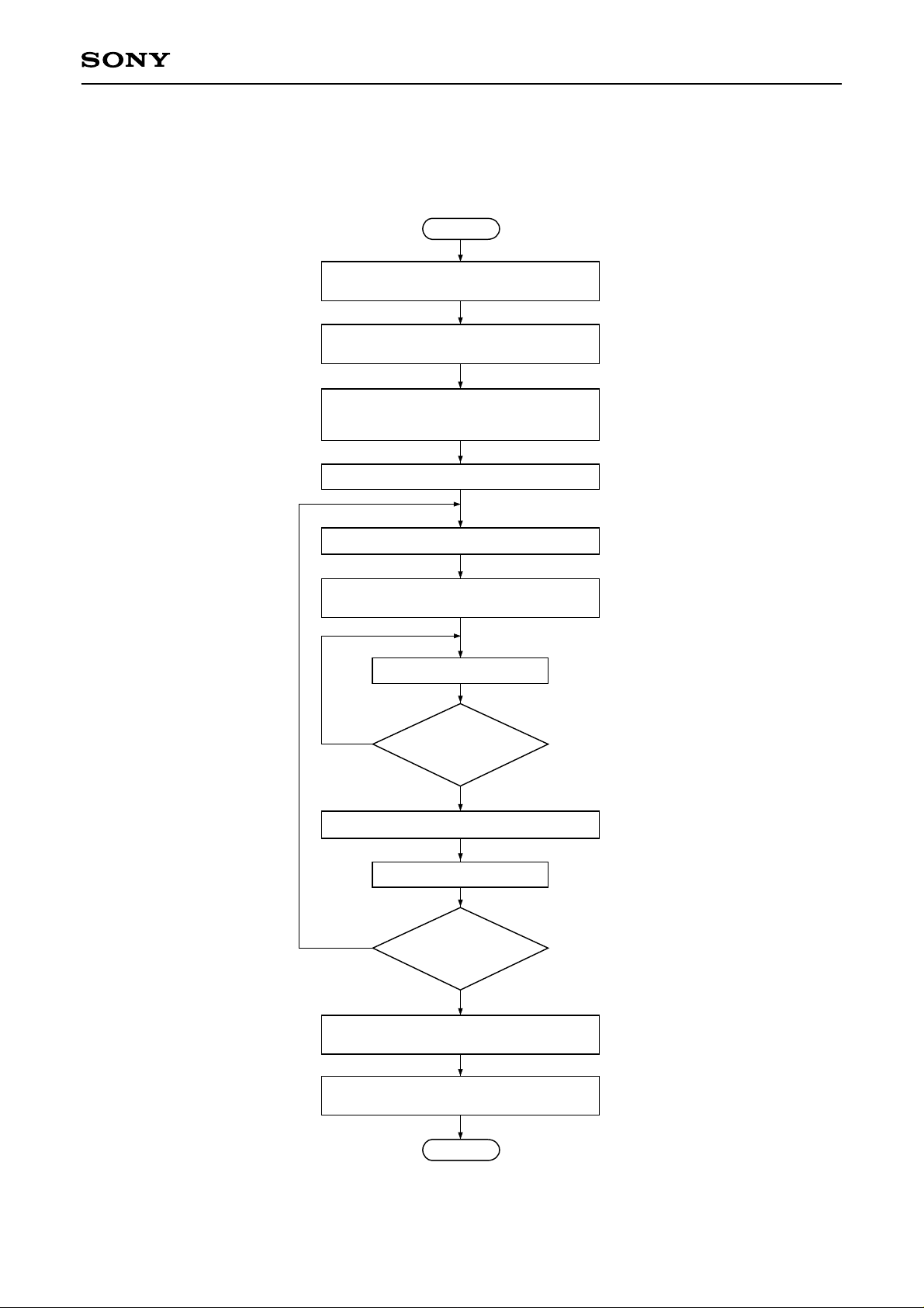
The following procedure is the procedure for setting gamma correction and color shading correction data from
an external EEPROM for forced refresh when power is turned on.
Start
During display, mute the video signal using the DSD
register.
Set GAM_ON = 0 and CSC_ON = 0 so that the
gamma RAMs and color shading RAMs are not used.
Set the GAM_ADDR, CSC_ADDR, CSC_SIZE and
ROM_TRAN registers to the addresses and transfer
count to be used to perform forced refresh.
Set the REF_RSEL register to gamma RAM (R).
Write "1" to the REF_END register and clear status.
Write 02h to the REF_MODE register to start forced
refresh.
Read the REF_END register.
Is the status "1"?
0: Forced refresh
currently being performed
Write "1" to the REF_END register and clear status.
Read the REF_RSEL register.
No
Is forced refresh
complete for all RAMs?
1: Forced refresh complete
Yes
Set GAM_ON and CSC_ON so that the gamma RAMs
and color shading RAMs will be used by the video signal.
If a video signal is to be displayed, cancel muting of
the video signal using the DSD register.
End
– 24 –
Page 25
CXD3526GG
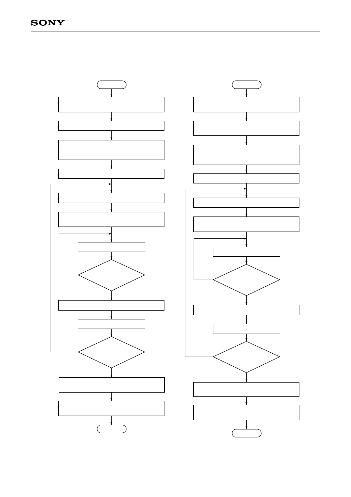
(5) Procedure for forced refresh during normal operations
The following procedure is the procedure for selecting either gamma correction or color shading correction
data during normal operations.
Start
During display, mute the video signal using the DSD
register.
Set GAM_ON = 0 so that the gamma RAMs are not used.
Set the GAM_ADDR and ROM_TRAN registers to the
addresses and transfer count to be used to perform
forced refresh.
Set the REF_RSEL register to gamma RAM (R).
Write "1" to the REF_END register and clear status.
Write 02h to the REF_MODE register to start forced
refresh.
Read the REF_END register.
Start
During display, mute the video signal using the DSD
register.
Set CSC_ON = 0 so that the color shading RAMs are
not used.
Set the CSC_ADDR, CSC_SIZE and ROM_TRAN
registers to the addresses and transfer count to be
used to perform forced refresh.
Set the REF_RSEL register to color shading RAM (R).
Write "1" to the REF_END register and clear status.
Write 02h to the REF_MODE register to start forced
refresh.
Read the REF_END register.
Is the status "1"?
0:Forced refresh
currently being performed
Write "1" to the REF_END register and clear status.
Read the REF_RSEL register.
Is forced refresh of the
Perform forced
refresh for the other
gamma RAMs.
Set GAM_ON so that the gamma RAMs will be used
by the video signal.
If a video signal is to be displayed, cancel muting of
the video signal using the DSD register.
gamma RAMs (R, G, B)
complete?
1: Forced refresh complete
Forced refresh complete
for all gamma RAMs.
End
Is the status "1"?
0: Forced refresh
currently being performed
Write "1" to the REF_END register and clear status.
Read the REF_RSEL register.
Is forced refresh of
the color shading RAMs
Perform forced
refresh for the other
color shading RAMs.
Set GAM_ON so that the color shading RAMs will be
used by the video signal.
If a video signal is to be displayed, cancel muting of
the video signal using the DSD register.
(R, G, B) complete?
1: Forced refresh complete
Forced refresh complete
for all color shading RAMs.
End
– 25 –
Page 26

CXD3526GG
(6) Procedure for self-refresh during normal operations
• Starting the refresh operation
The following procedure is the procedure used to set cyclic refreshing of the gamma correction and color
shading correction data stored in the built-in RAM during normal operations.
Start
Set the GAM_H1, GAM_H2, GAM_V1 and GAM_V2 registers of the DSD
register and the CSC_HNUM, CSC_VNUM, CSC_HINT and CSC_VINT
registers of the color shading register to the appropriate values.
Set GAM_ON and CSC_ON so that the gamma RAMs and color shading
RAMs are used by the video signal.
Set the GAM_ADDR, CSC_SIZE and ROM_TRAN registers to the
addresses and transfer count to be used to perform self-refresh.
Set the REF_RSEL register to gamma RAM (R).
Write "1" to the REF_END register and clear status.
Write 01h to the REF_MODE register and start self-refresh.
End
• Stopping the refresh operation
The following procedure is the procedure used to stop the self-refresh operation.
Start
Write 00h to the REF_MODE register to stop self-refresh.
End
– 26 –
Page 27

CXD3526GG
4. Timing Generator (TG) Block
This block generates the timing pulses required to drive Sony LCD panels. Of the output pulses, the required
pulses differ according to the LCD panel type, so be sure to also check the specifications of the panel used.
The output timing pulses are all set by the serial bus. For a detailed description, see the description of the TG
block register setting.
HSYNC
VSYNC
HSYNC
Detector
HPOL
Detector
VSYNC
Detector
VPOL
Detector
PLL Counter
N Detector
Register
Pic. PLS
HPOS. Counter
HPLS
Generator
VPLS GeneratorHPOS. Counter
HST, PST, HCK1, HCK2,
DCK1, DCK2, ENB, PCG,
PRG, SHST, HD2, HD3,
CLR
CLP, HD1
VST , VCK,
FRP, XFRP
CTRL
RGT, DWN
XRGT, PO1, PO2
– 27 –
Page 28

5. DSD Block
The DSD block signal processing flow is shown below.
CXD3526GG
R, G, B IN
10
User gain Sub gainUser bright Sub bright
YS, YM
R, G, B OSD
Pattern
generator
Color shading
correction
OSD
Mute 2 Limiter
Gamma
correction
Ghost
cancel
Gamma
gain
Black
frame
Cycle offset
Mute 1
Gamma
bright
10
R, G, B OUT
The various signal processing functions are described below. Note that the coefficients used for each
arithmetic operation are set through the host I/F. See the descriptions of the DSD block register setting.
(a) User gain
This block performs multiplication processing as the user control gain adjustment. The settings are as follows.
Coefficient: 8 bits
Gain setting: 0 to 3.984375 (= 255/64) times, variable in 256 steps
(Settings shared by R, G and B)
Multiplication is performed using the 10-bit input and an 8-bit coefficient, and the upper 13 bits c[17:5] of the
operation results are output. Next, the c[5] value is checked and rounding is performed to 12 bits. The upper
2 bits of the rounded 12 bits is checked, clipping is perfor med, and the lower 10 bits are output.
Coefficient
b[7:0]
8
10 13
Input
a[9:0]
a × b
c[17:5]
Rounding
and
clipping
10
Output
– 28 –
Page 29
CXD3526GG
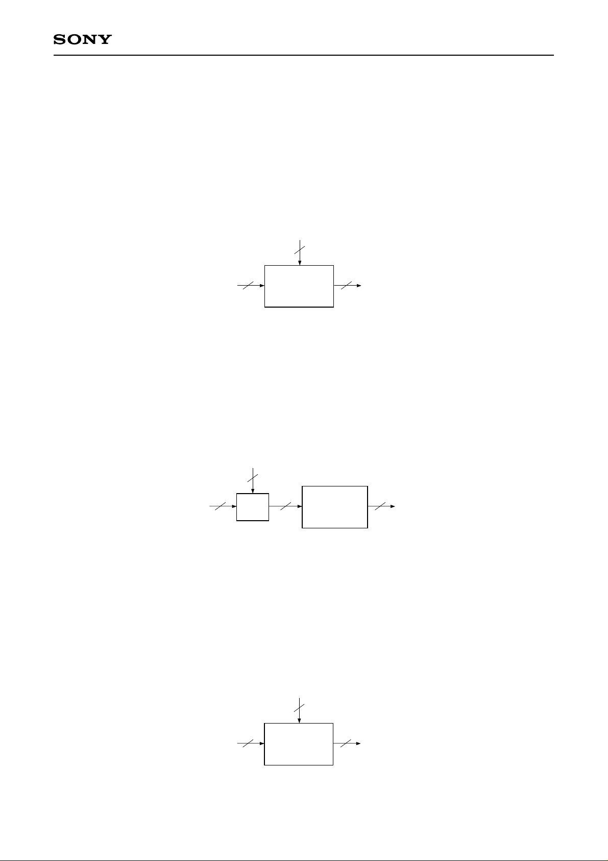
(b) User bright
This block performs addition and subtraction processing as the user control bright adjustment. The settings are
as follows.
Coefficient: 11 bits with code, MSB = code bit
Bright setting: –1024 to +1023 graduation, var iable with an accuracy of 1 bit
(Settings shared by R, G and B)
Multiplication is performed using the 10-bit input and an 11-bit coefficient with code. The coefficient MSB is the
code bit. Addition is performed when b[10] = 0, and subtraction when b[10] = 1. However, when perfor ming
subtraction, set the two's complement in the lower bits of the coefficient. When the operation results overflow
or underflow, clipping is performed.
Coefficient
b[10:0]
10 10
Input
a[9:0]
11
Addition/subtraction
and
clipping
Output
(c) Sub gain
This block performs multiplication processing as the white balance gain adjustment. The settings are as follows.
Coefficient: 8 bits
Gain setting: 0 to 3.984375 (255/64) times, variable in 256 steps
(Set independently for R, G and B)
Multiplication is performed using the 10-bit input and an 8-bit coefficient, and the upper 13 bits c[17:5] of the
operation results are output. Next, the c[5] value is checked and rounding is performed to 12 bits. The upper 2
bits of the rounded 12 bits is checked, clipping is perfor med, and the lower 10 bits are output.
Coefficient
b[7:0]
10 13 10
Input
a[9:0]
8
a × b
c[17:5]
Rounding
and
clipping
Output
(d) Sub bright
This block perfor ms addition and subtraction processing as the white balance br ight adjustment. The settings
are as follows.
Coefficient: 11 bits with code, MSB = code bit
Bright setting: –1024 to +1023 graduation, var iable with an accuracy of 1 bit
(Set independently for R, G and B)
Multiplication is performed using the 10-bit input and an 11-bit coefficient with code. The coefficient MSB is the
code bit. Addition is performed when b[10] = 0, and subtraction when b[10] = 1. However, when perfor ming
subtraction, set the two's complement in the lower bits of the coefficient. When the operation results overflow
or underflow, clipping is performed.
Input
a[9:0]
Coefficient
b[10:0]
10 10
11
Addition/subtraction
and
clipping
Output
– 29 –
Page 30
CXD3526GG
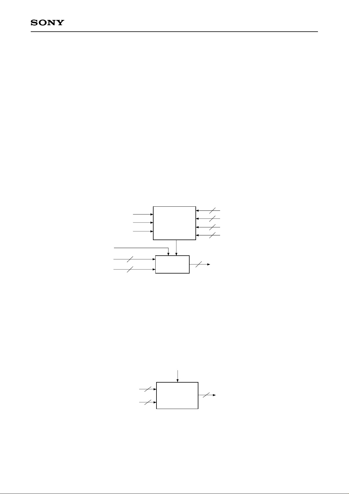
(e) Black frame
This block perfor ms processing to fix the blanking period of the video signal to the desired level regardless of
the front-end signal processing results.
If the number of pixels calculated from the effective period of the video signal to be displayed is less than the
number of pixels of the LCD panel on which the signal is to be displayed, the blanking period of the video
signal is displayed in the excess pixels. At this time, the displayed blanking period can be fixed to the desired
level regardless of the gain and bright adjustment or other picture quality adjustment results by processing with
this block. The settings are as follows.
FRM_ON: 1 = Black frame processing ON, 0 = OFF
FRM_DAT: Black frame level setting
FRM_H1, FRM_H2: Set the black frame horizontal display range in 1-dot units
FRM_V1, FRM_V2: Set the black frame vertical display range in 1-line units
(All settings shared by R, G and B)
Here, the desired range of the video signal is replaced with 10-bit data (FRM_DAT) by switching the video
signal and the coefficients using the pulse output from the pulse decoder.
Internal HD
Internal VD
Internal MCLK
Processing ON/OFF
Input
Coefficient
10
10
Pulse decoder
Selector
11
11
11
11
10
Horizontal display range 1
Horizontal display range 2
Vertical display range 1
Vertical display range 2
Output
(f) Mute 1
This block performs mute processing by replacing the video signal with data of the desired level. The settings
are as follows.
MUTE1_ON: 1 = Mute processing ON, 0 = OFF (Settings shared by R, G and B)
R, G, B_MUTE1: RGB mute data (Set independently for R, G and B)
Processing ON/OFF
Input
Coefficient
10
10
Selector
– 30 –
10
Output
Page 31
CXD3526GG
(g) Pattern generator
This block generates and outputs the set fixed pattern independently of the input signal. This function is valid
when PG_ON = 1. When PG_R (G, B)_ON is "0", the signal level goes to 000h respectively for R, G and B.
The raster display pattern is displayed in the effective area, and all other display patterns are displayed in the
window area. Here, the effective area is set by PG_HST, PG_HSTP, PG_VST and PG_VSTP, and the window
area is set by PG_HWST, PG_HWSTP, PG_VWST and PG_VWSTP.
The display pattern signal level is set independently for R, G and B by PG_SIG1R (G, B)[9:0] and PG_SIG2R
(G, B)[9:0]. Within the effective area, the pattern and non-pattern signal levels can be switched by PG_R (G,
B)_SEL. At this time, the signal level outside the effective area goes to 000h. During horizontal ramp, horizontal
stair, vertical ramp and vertical stair display, the PG_SIG1R (G, B)[9:0] and PG_SIG2R (G, B)[9:0] settings are
invalid.
The display patterns and signal levels are as follows.
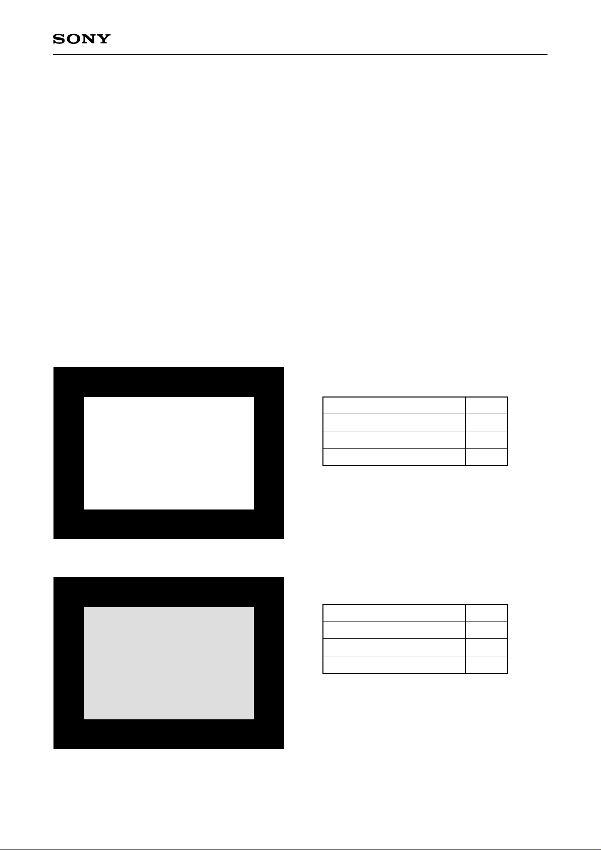
(1) Raster display
When PG_PAT[2:0] = 0h, a raster is displayed.
PG_SIG2R (G, B)
PG_R (G, B)_SEL
PG_PAT[2:0]
PG_STRP_SW
PG_STAIR_SW
PG_R (G, B)_SEL
PG_PAT[2:0]
0
0h
x
x
1
0h
PG_SIG1R (G, B)
– 31 –
PG_STRP_SW
PG_STAIR_SW
x
x
x: Don't care
Page 32

(2) Window display
When PG_PAT[2:0] = 1h, a window is displayed.
CXD3526GG
PG_SIG2R (G, B)
PG_SIG1R (G, B)
PG_SIG1R (G, B)
PG_SIG2R (G, B)
PG_R (G, B)_SEL
PG_PAT[2:0]
PG_STRP_SW
PG_STAIR_SW
PG_R (G, B)_SEL
PG_PAT[2:0]
PG_STRP_SW
PG_STAIR_SW
0
1h
x
x
1
1h
x
x
– 32 –
x: Don't care
Page 33
CXD3526GG
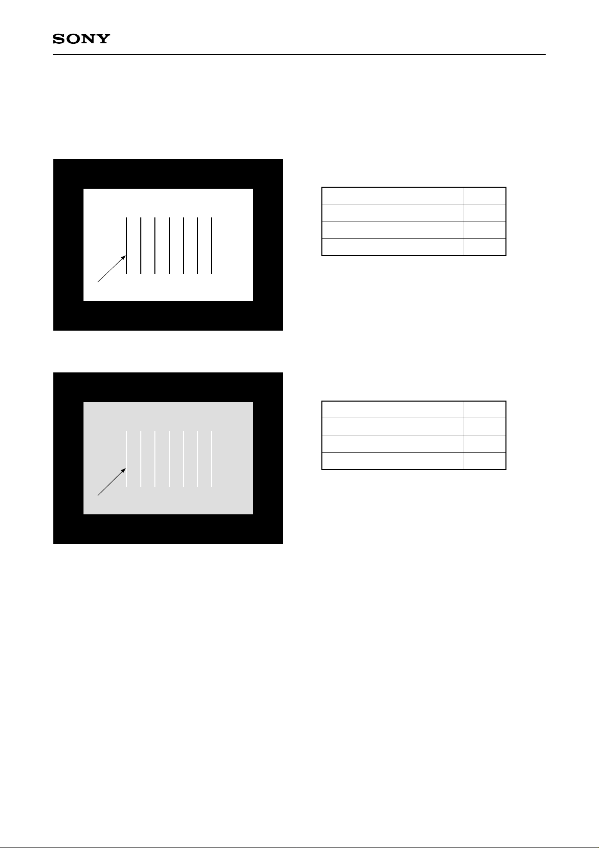
(3) Vertical stripe display
When PG_PAT[2:0] = 2h and PG_STRP_SW = 0, vertical stripes are displayed.
The stripe period is set by PG_STEP in 1-dot units. The stripe width is set by PG_WIDTH in 1-dot units.
PG_SIG2R (G, B)
PG_SIG1R (G, B)
PG_SIG1R (G, B)
PG_R (G, B)_SEL
PG_PAT[2:0]
PG_STRP_SW
PG_STAIR_SW
PG_R (G, B)_SEL
PG_PAT[2:0]
PG_STRP_SW
PG_STAIR_SW
0
2h
0
x
1
2h
0
x
PG_SIG2R (G, B)
x: Don't care
– 33 –
Page 34

CXD3526GG
(4) Diagonal stripes display
When PG_PAT[2:0] = 2h and PG_STRP_SW = 1, diagonal stripes are displayed.
The stripe period is set by PG_STEP in 1-dot units. The stripe width is set by PG_WIDTH in 1-dot units.
PG_SIG2R (G, B)
PG_SIG1R (G, B)
PG_SIG1R (G, B)
PG_R (G, B)_SEL
PG_PAT[2:0]
PG_STRP_SW
PG_STAIR_SW
PG_R (G, B)_SEL
PG_PAT[2:0]
PG_STRP_SW
PG_STAIR_SW
0
2h
1
x
1
2h
1
x
PG_SIG2R (G, B)
x: Don't care
– 34 –
Page 35
CXD3526GG
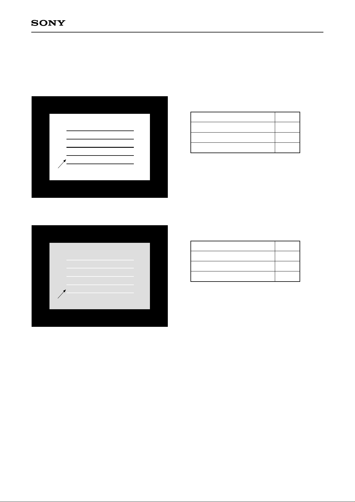
(5) Horizontal stripes display
When PG_PAT[2:0] = 3h, horizontal stripes are displayed.
The stripe period is set by PG_STEP in 1-dot units. The stripe width is set by PG_WIDTH in 1-dot units.
PG_SIG2R (G, B)
PG_SIG1R (G, B)
PG_SIG1R (G, B)
PG_R (G, B)_SEL
PG_PAT[2:0]
PG_STRP_SW
PG_STAIR_SW
PG_R (G, B)_SEL
PG_PAT[2:0]
PG_STRP_SW
PG_STAIR_SW
0
3h
x
x
1
3h
x
x
PG_SIG2R (G, B)
x: Don't care
– 35 –
Page 36
CXD3526GG
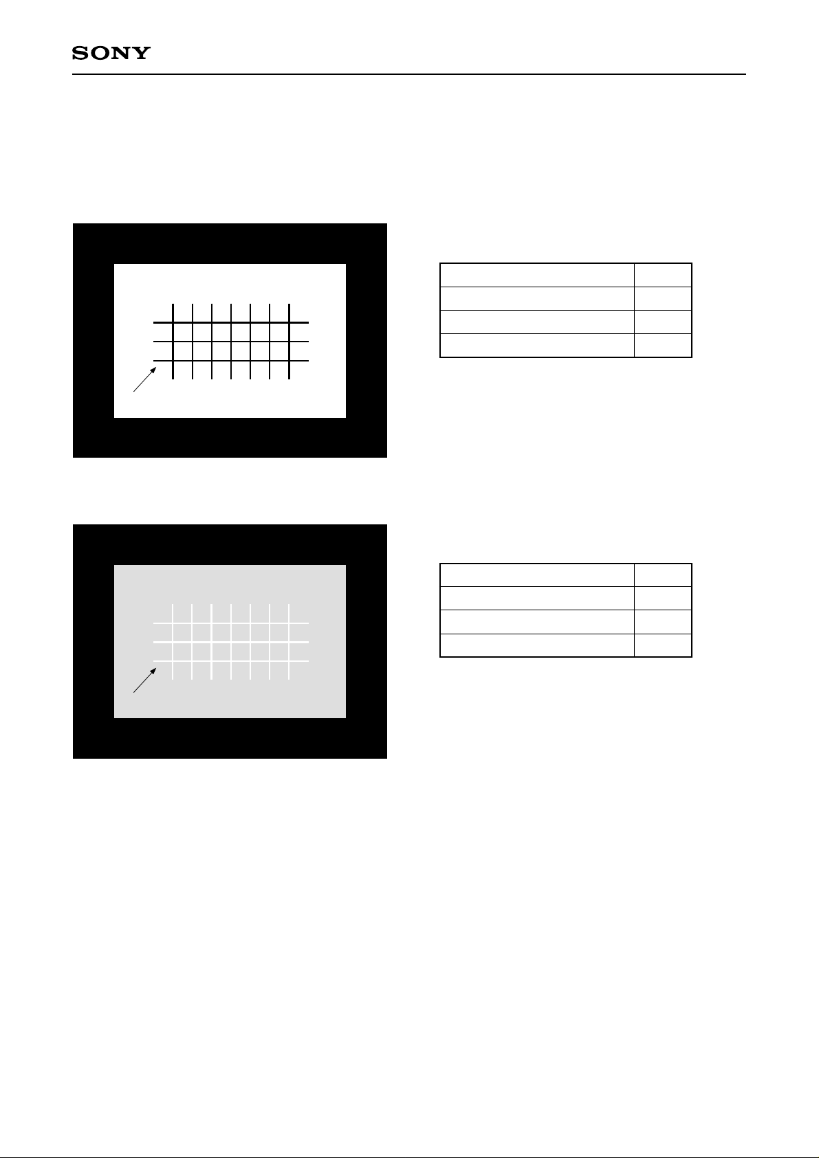
(6) Cross hatch display
When PG_PAT[2:0] = 4h, a cross hatch is displayed.
The stripe period is set by PG_STEP in 1-dot units. The stripe width is set by PG_WIDTH in 1-dot units.
PG_SIG2R (G, B)
PG_SIG1R (G, B)
PG_SIG1R (G, B)
PG_R (G, B)_SEL
PG_PAT[2:0]
PG_STRP_SW
PG_STAIR_SW
PG_R (G, B)_SEL
PG_PAT[2:0]
PG_STRP_SW
PG_STAIR_SW
0
4h
x
x
1
4h
x
x
PG_SIG2R (G, B)
x: Don't care
– 36 –
Page 37
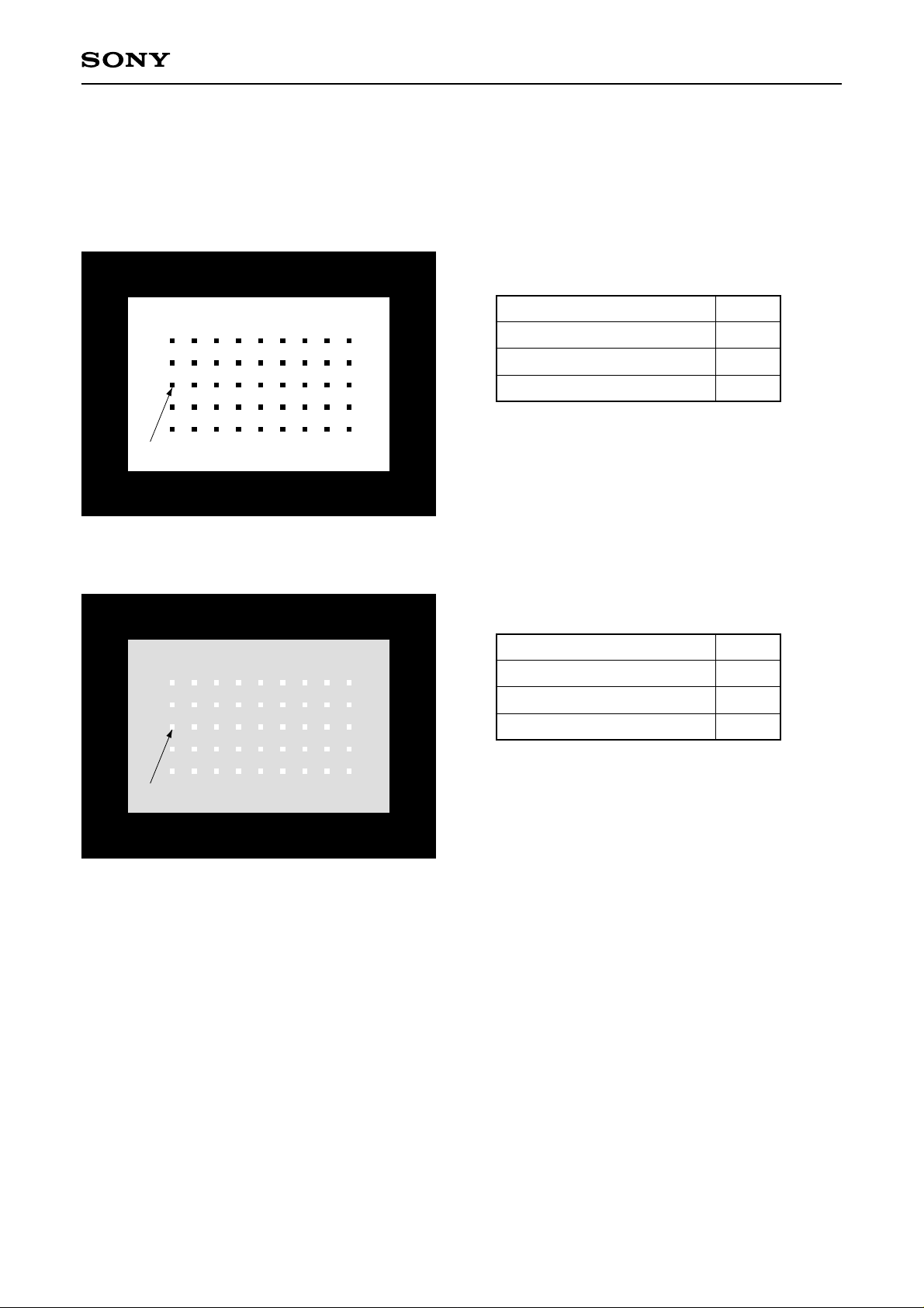
(7) Dots display
When PG_PAT[2:0] = 5h, a dot pattern is displayed.
The dot period is set by PG_STEP in 1-dot units. The dot width is set by PG_WIDTH in 1-dot units.
CXD3526GG
PG_SIG2R (G, B)
PG_SIG1R (G, B)
PG_SIG1R (G, B)
PG_R (G, B)_SEL
PG_PAT[2:0]
PG_STRP_SW
PG_STAIR_SW
PG_R (G, B)_SEL
PG_PAT[2:0]
PG_STRP_SW
PG_STAIR_SW
0
5h
x
x
1
5h
x
x
PG_SIG2R (G, B)
x: Don't care
– 37 –
Page 38
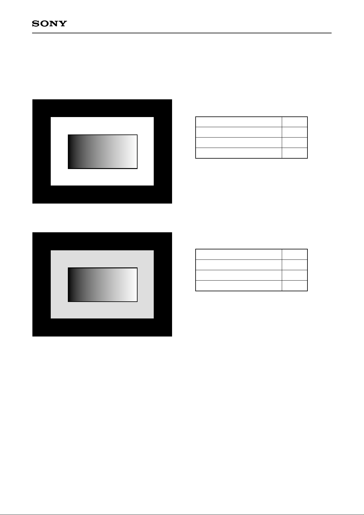
(8) Horizontal ramp display
When PG_PAT[2:0] = 6h and PG_STAIR_SW = 0, a horizontal ramp is displayed.
The signal level is incremented from 000h by one graduation for each dot.
CXD3526GG
PG_SIG2R (G, B)
PG_SIG1R (G, B)
PG_R (G, B)_SEL
PG_PAT[2:0]
PG_STRP_SW
PG_STAIR_SW
PG_R (G, B)_SEL
PG_PAT[2:0]
PG_STRP_SW
PG_STAIR_SW
0
6h
x
0
1
6h
x
0
– 38 –
x: Don't care
Page 39
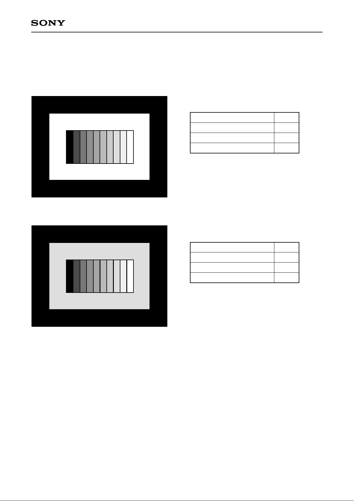
(9) Horizontal stair display
When PG_PAT[2:0] = 6h and PG_STAIR_SW = 1, a horizontal stair is displayed.
The signal level is incremented from 000h by 64 graduation for each 64 dots.
CXD3526GG
PG_SIG2R (G, B)
PG_SIG1R (G, B)
PG_R (G, B)_SEL
PG_PAT[2:0]
PG_STRP_SW
PG_STAIR_SW
PG_R (G, B)_SEL
PG_PAT[2:0]
PG_STRP_SW
PG_STAIR_SW
0
6h
x
1
1
6h
x
1
– 39 –
x: Don't care
Page 40
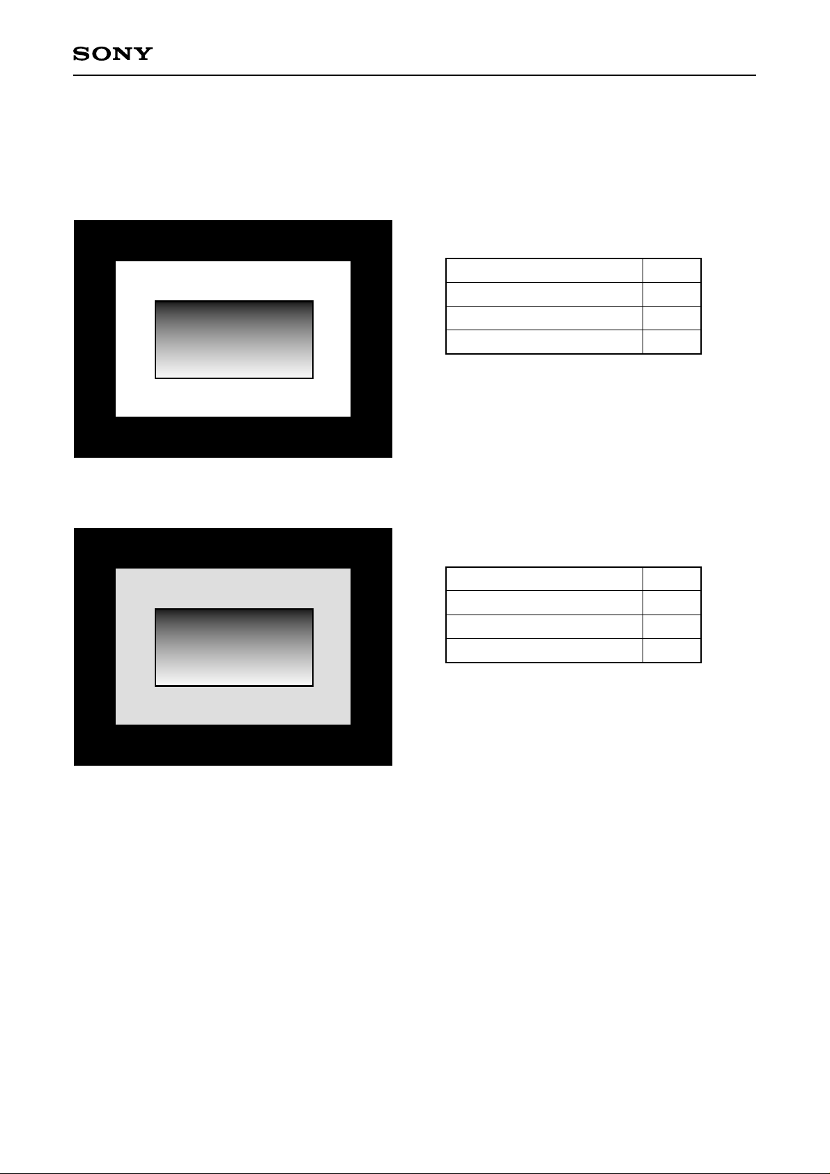
(10) Vertical ramp display
When PG_PAT[2:0] = 7h and PG_STAIR_SW = 0, a vertical ramp is displayed.
The signal level is incremented from 000h by one graduation for each line.
CXD3526GG
PG_SIG2R (G, B)
PG_SIG1R (G, B)
PG_R (G, B)_SEL
PG_PAT[2:0]
PG_STRP_SW
PG_STAIR_SW
PG_R (G, B)_SEL
PG_PAT[2:0]
PG_STRP_SW
PG_STAIR_SW
0
7h
x
0
1
7h
x
0
– 40 –
x: Don't care
Page 41
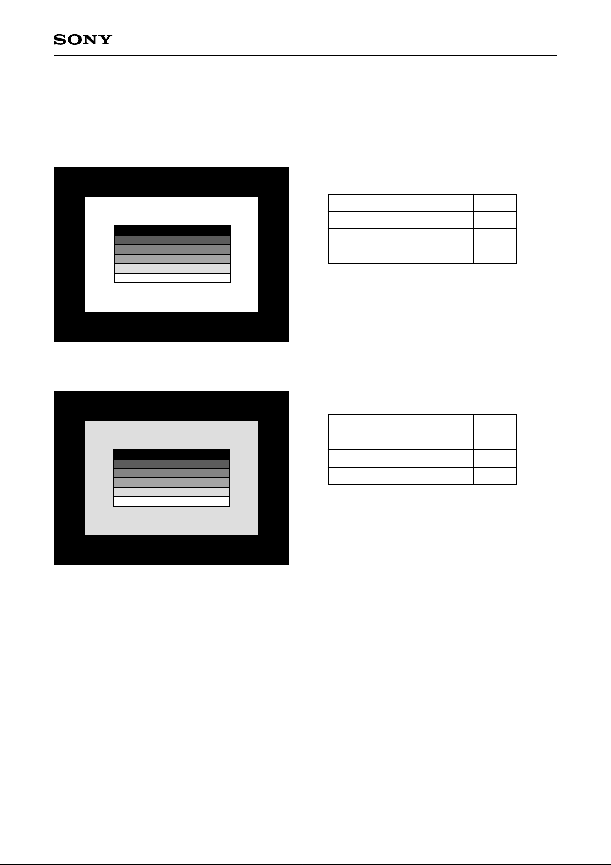
(11) Vertical stair display
When PG_PAT[2:0] = 7h and PG_STAIR_SW = 1, a vertical stair is displayed.
The signal level is incremented from 000h by 64 graduation for each 32 lines.
CXD3526GG
PG_SIG2R (G, B)
PG_SIG1R (G, B)
PG_R (G, B)_SEL
PG_PAT[2:0]
PG_STRP_SW
PG_STAIR_SW
PG_R (G, B)_SEL
PG_PAT[2:0]
PG_STRP_SW
PG_STAIR_SW
0
7h
x
1
1
7h
x
1
– 41 –
x: Don't care
Page 42
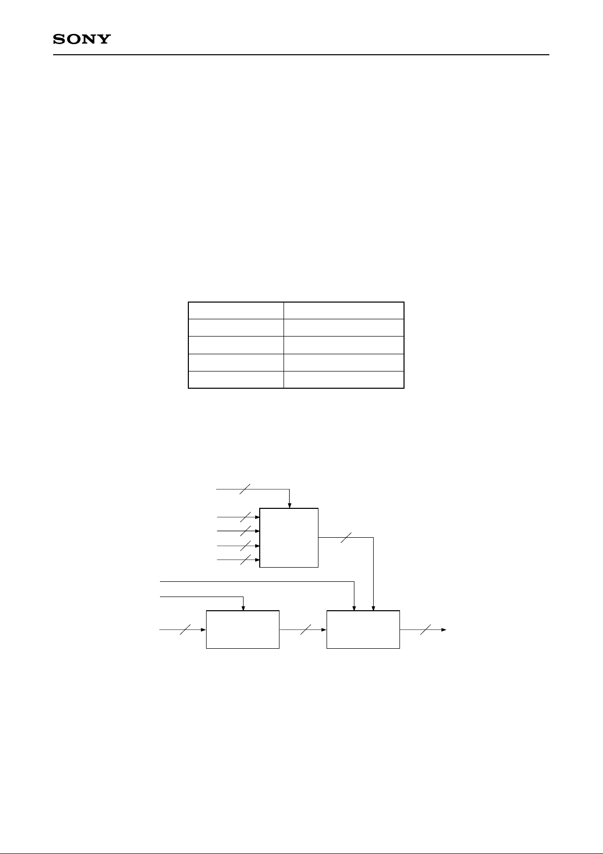
CXD3526GG
(h) OSD
This block performs video signal half-tone processing and OSD_MIX processing by inputting the 2-bit OSD
signal for each color and the YS and YM signals. The half-tone processing setting is as follows.
YM signal input: 1 = Half-tone processing ON, 0 = OFF
Here, the video signal level is halved by shifting the input data by one bit to the LSB side when YM = 1. For
example, when 0F0h is input, 078h is output.
The selector selects one of four types of data with respect to the OSD signal value as shown in the table
below. The selected data becomes the OSD signal gradual data. The selected gradual data can be set
independently in 10 bits for R, G and B, so 4 graduation can be selected as desired from among 1024
graduation for each of R, G and B. Therefore, the desired 64 (= 2^6) colors can be selected from among the
total 1.07374 billion (= 2^30) colors for R, G and B.
OSD signal input
0h
1h
2h
3h
The OSD_MIX processing setting is as follows.
YS signal input: 1 = OSD_MIX processing ON, 0 = OFF
OSD signal
Gradual data 1
Gradual data 2
Gradual data 3
Gradual data 4
YS signal
YM signal
2
10
10
10
10
Selected gradual data
R, G, B_OSD_DAT1
R, G, B_OSD_DAT2
R, G, B_OSD_DAT3
R, G, B_OSD_DAT4
Selector
10
Input Output
Half-tone
processing
10
OSD_MIX
1010
– 42 –
Page 43
CXD3526GG
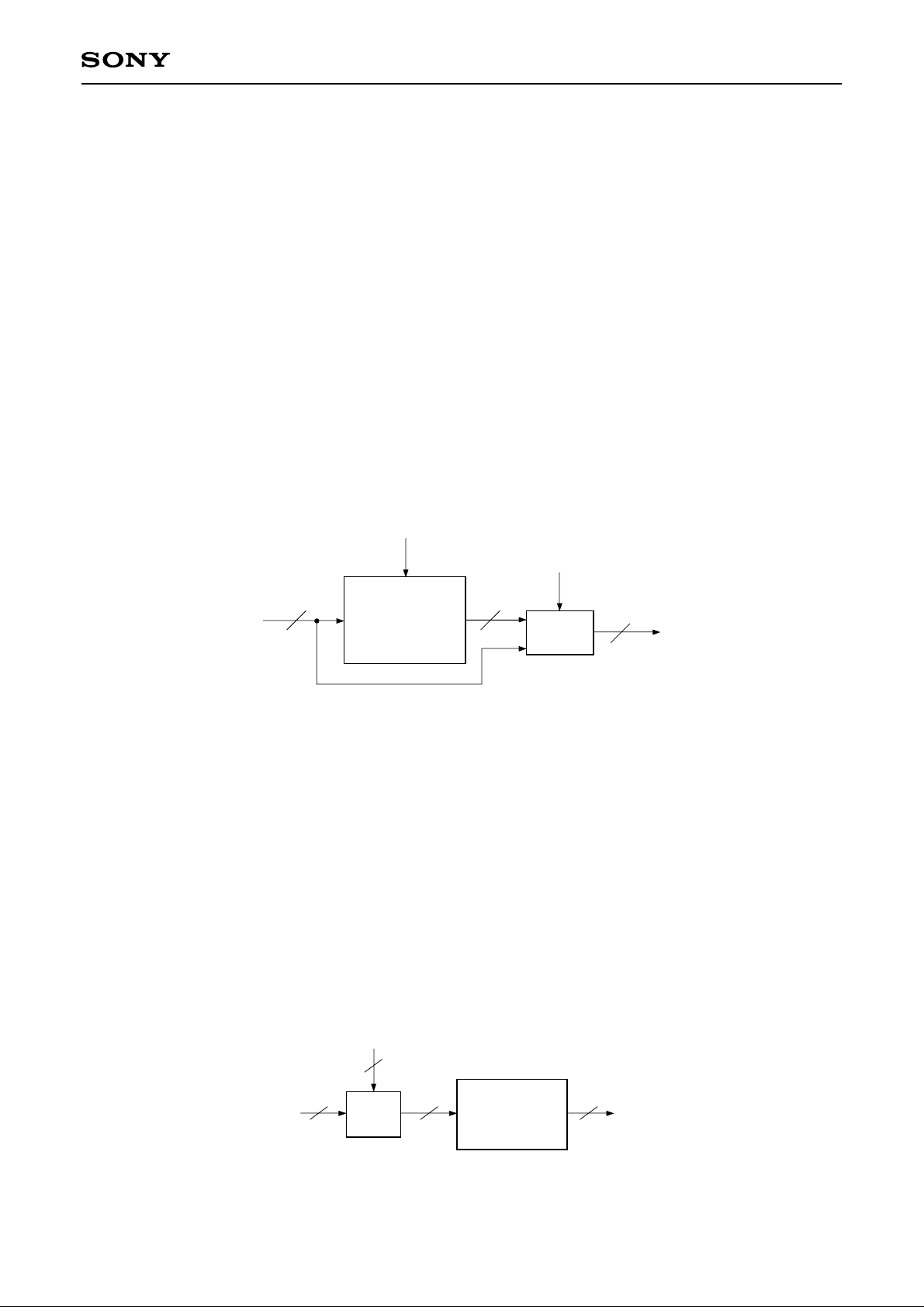
(i) Gamma correction
This block perfor ms gamma correction for the user- and white balance-adjusted signal. Gamma correction
uses the LUT system, and the RAM size is 10 bits × 1024 words. The settings are as follows.
GAM_ON: 1 = Gamma correction processing ON, 0 = Gamma correction processing OFF
GAM_MODE: 1 = Normal operation mode, 0 = Power-saving mode
GAM_H1, GAM_H2: 1 = Gamma correction processing range is set in 1-dot units
GAM_V1, GAM_V2: 1 = Gamma correction processing range is set in 1-line units
(All settings shared by R, G and B)
When operating the RAM, be sure to set GAM_MODE = 1. Data cannot be written to or read from the RAM in
power-saving mode. The RAM data is set through the host I/F block or exter nal ROM I/F.
Set gamma correction processing range (effective period of video signal) to GAM_H1 and GAM_H2, and
GAM_V1, GAM_V2. This setting enables access to RAM from serial bus.
Note that the RAM output is undetermined during power-on.
RAM ON/OFF
Data path selection
Input
10 10
RAM
10 bits × 1024 words
Selector
10
Output
(j) Gamma gain
This block performs multiplication processing to correct VT curve variation of the LCD panel as gain adjustment
for the gamma corrected signal. The settings are as follows.
Coefficient: 8 bits
Gain setting: 0 to 1.9921875 (= 255/128) times, variable in 256 steps
(Set independently for R, G and B)
Multiplication is performed using the 10-bit input and an 8-bit coefficient, and the upper 12 bits c[17:6] of the
operation results are output. Next, the c[6] value is checked and rounding is performed to 11 bits. The MSB of
the rounded 11 bits is checked, clipping is perfor med, and the lower 10 bits are output.
Coefficient
b[7:0]
10 12 10
Input
a[9:0]
8
a × b
Rounding
and
clipping
c[17:6]
– 43 –
Output
Page 44
CXD3526GG
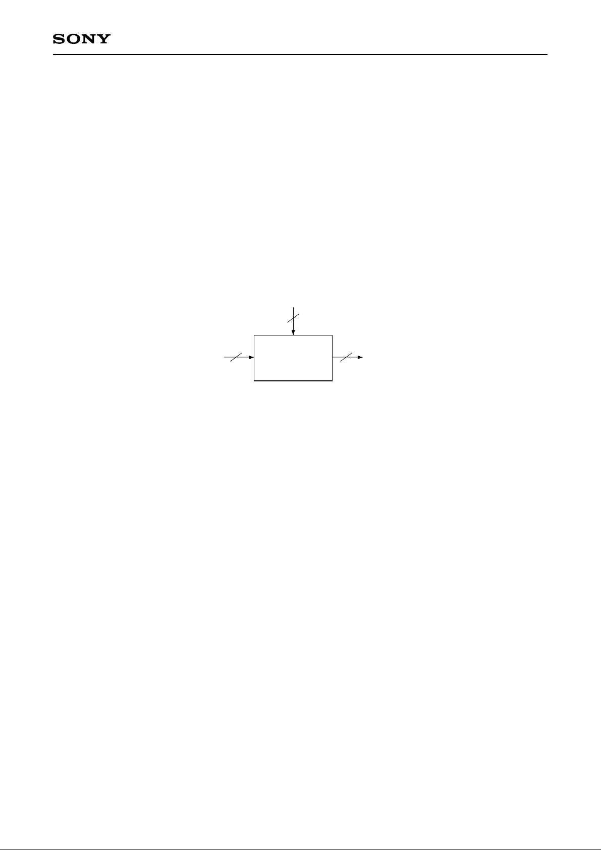
(k) Gamma bright
This block perfor ms addition and subtraction processing to correct VT curve variation of the LCD panel as
bright adjustment for the gamma corrected signal. The settings are as follows.
Coefficient: 11 bits with code, MSB = code bit
Bright setting: –1024 to +1023 graduation, va riable with an accuracy of 1 bit
(Set independently for R, G and B)
Multiplication is performed using the 10-bit input and a 11-bit coefficient with code. The coefficient MSB is the
code bit. Addition is performed when b[10] = 0, and subtraction when b[10] = 1. However, when perfor ming
subtraction, set the two's complement in the lower bits of the coefficient. When the operation results overflow
or underflow, clipping is performed.
Coefficient
b[10:0]
11
10 10
Input
a[9:0]
Addition/subtraction
and
clipping
Output
– 44 –
Page 45

CXD3526GG
(l) Color shading correction
This block corrects color shading by adding a correction signal to the video signal. Correction points are set at
fixed intervals in the horizontal, vertical and gradual directions of the video signal. The correction data for these
correction points is written in the RAM, and a correction curve is created by reading this data and performing
interpolation operations. The settings are as follows.
CSC_ON: 1 = Color shading correction processing ON, 0 = Processing OFF
CSC_R (G, B)_RGT∗: 1 = Reflects the TG block RGT setting,
0 = Reflects the inverse of the TG block RGT setting
CSC_DWN: 1 = Reflects the TG block DWN setting,
0 = Reflects the inverse of the TG block DWN setting
CSC_HP: Sets the horizontal correction start position
CSC_VP: Sets the vertical correction start position
CSC_HNUM: Sets the number of horizontal correction points
CSC_VNUM: Sets the number of vertical correction points
CSC_HINT: Sets the horizontal correction interval
CSC_VINT: Sets the vertical correction interval
CSC_HOS: Sets the expansion of the horizontal correction area
CSC_VOS: Sets the expansion of the vertical correction area
CSC_GNUM: Sets the gradual correction points
CSC_R (G, B) GP1 to 8∗: Sets the gradual correction points
CSC_R (G, B) GD1 to 8∗: Sets the expansion of the correction data
CSC_XH_ON: 1 = Cross hatch insertion ON, 0 = OFF
CSC_XH_DAT: Sets the cross hatch display level
∗
: Set independently for R, G and B, Others: Settings shared by R, G and B
The color shading correction data of the desired gradual level up to 8 screens (max.) can be set in RAM. The
RAM size is 8 bits × 1792 words, so up to 1792 correction points can be set. The correction data is set as 8-bit
data with code. Correction data can be set in the range of –128 to +127 graduation. The example shown on
page 47 is for a 1024-dot × 768-line XGA video signal divided into 9 points at 128-dot intervals in the horizontal
direction and 7 points at 128-line intervals in the vertical direction. The relationship between the correction
point coordinates (m, n) and the RAM address is obtained as follows.
RAM address = (m – 1) + (n – 1) × (Number of horizontal correction points)
For the example on page 47, this is as follows.
(9 – 1) + (7 – 1) × 9 = 62
Thus, the correction data must be set in the RAM from address 0 to address 62.
– 45 –
Page 46
CXD3526GG
If correction is to be performed in the gradual direction as well, the RAM address is found based on the
relationship between the coordinates (m, n) of the correction points and the number of gradual correction
points using the formula below:
RAM address = (m – 1) + (n – 1) × (number of horizontal correction points)
+ (number of horizontal correction points) × (number of vertical correction points)
× (number of gradual correction points – 1)
If the number of gradual correction points is eight, it is necessary to set correction data into RAM from Address
0 to Address 503 as calculated below:
(9 – 1) + (7 – 1) × 9 + 9 × 7 × 7 = 503
Correction data in the gradual direction for the screen 2 and subsequent planes is set in order from Address 63.
This IC supports top/bottom and/or right/left inversion of the LCD panel by controlling the direction in which
correction data that has been set into RAM is read. Up/down and/or right/left inversion are set from DWN and
RGT of the TG block.
CSC_DWN and CSC_R (G, B)_RGT control the link with the TG block settings. It is therefore unnecessary to
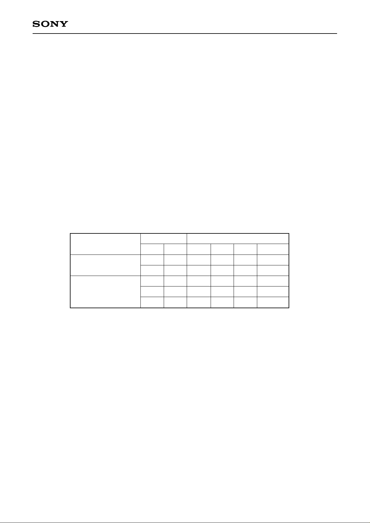
reset correction data. The table below gives an example of setting correction points.
Signal specification
XGA (1024 × 768)
SVGA (800 × 600)
Correction gap Number of correction points
H
64
64
50
64
64
V
64
64
50
64
64
HV
17
16
17
14
13
13
12
13
11
10
Example of Setting Correction Points
G
8
8
8
8
8
Total
1768
1536
1768
1232
1040
– 46 –
Page 47
CXD3526GG
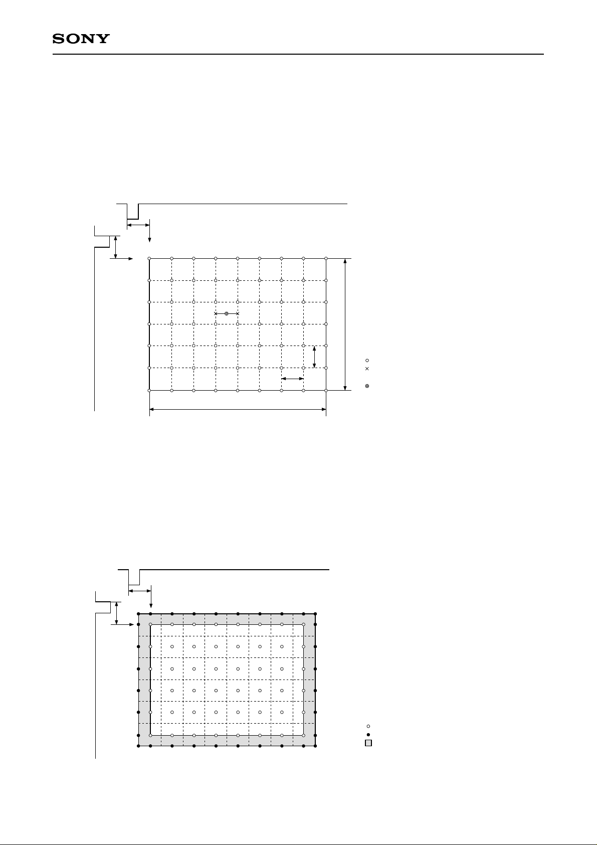
This IC has two ways it can handle interpolation in the horizontal and vertical directions: by dividing the screen
into a uniform grid and setting data for points at the intersections or by setting data for points in the center of
each area.
(1) When setting data for intersection points (pixels) on the screen
The correction area is set for the entire screen. An interpolation operation uses 4 values nearby
intermediate points to perform calculations. The correction start position is set using CSC_HP and CSC_VP.
Be sure to set the start position for the effective period of the video signal.
HDIN
Correction start position
VDIN
1
1
2
3
4
Correction start position
5
6
7
Number of correction points
(m, n)
Correction interval (128 dots)
1024 dots
Number of correction points
98765432
Correction interval (128 lines)
768 lines
: Correction data that has been set in RAM
: Interpolation operation results for the vertical
direction
: Interpolation operation results for the horizontal
direction
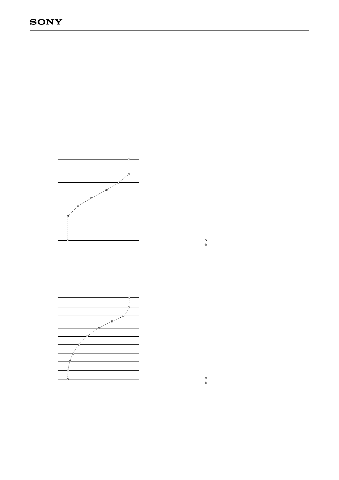
(2) When setting the correction point to the center of the areas dividing the screen
The correction area is set to inside the screen. At this time, be sure to set the correction start position so it
lies inside the screen. When the correction point is set to the center of the areas dividing the screen, it is
necessary to virtually perform correction outside the correction area for which correction data is set. It is
therefore assumed that the same data as at the edge of the correction area applies to outside the
interpolation area, and linear inter polation is performed.
Use CSC_HOS and CSC_VOS to set correction areas that are to be expanded.
HDIN
Correction start position
VDIN
Correction start position
: Correction data that has been set in RAM
: Data assumed to lie in invalid period
: Area to be virtually corrected
– 47 –
Page 48
CXD3526GG
The number of correction points to be used by this IC for correction in the gradual direction can be set using
CSC_GNUM. The number of correction points can be var ied from 1 to 8 and settings are available for each
RGB signal. This means that the gradual level for which correction is to be performed can be independently
and freely set for each RGB signal using CSC_R (G, B) GP1 to 8. An inter polation operation uses 2 values
nearby intermediate points to perform linear interpolation.
If the number of correction points is 1, no interpolation operation is performed in the gradual direction. The
results of interpolation for one screen are added to the video signal regardless of the gradual level of the video
signal being input. Correction data for one screen is entered into RAM beginning from Address 0.
When two or more correction points are used, interpolation in the gradual direction is performed according to the
gradual level of the video signal being input. If the number of correction points is 2 through 7, be sure to set data
into RAM for the number of screens equal to "the number of correction points plus 1", beginning from Address 0.
In the example shown in the figure belo w, correction data is assigned when there are 5 correction points. In addition
to the 5 correction points, data for Screen 1 (Correction Point 1) is assigned to 3FFh. Data for the Screen 6
(Correction Point 6) is assigned to 000h. In the case of the Screen 6, be sure to either set correction data for
gradual level 000h or the same correction data as for Screen 5. In this time the value set by using CSC_R (G, B)
GP6 is ignored.
3FFh
Data for Screen 1
(Correction Point 1)
300h
200h
100h
000h
Screen 1 (Correction Point 1)
Screen 2 (Correction Point 2)
Screen 3 (Correction Point 3)
Screen 4 (Correction Point 4)
Screen 5 (Correction Point 5)
Data for Screen 6
(Correction Point 6)
: Correction data that has been set in RAM
: Interpolation operation results for the gradual direction
Example of Settings for Five Correction Points
When there are 8 correction points, be sure to set the data for the 8 screens into RAM beginning from Address 0.
In addition to the 8 correction points, data for Screen 1 (Correction Point 1) is assigned to 3FFh as shown in the
figure below. Data for Screen 8 (Correction Point 8) is assigned to 000h.
3FFh
300h
200h
100h
000h
Data for Screen 1
(Correction Point 1)
Screen 1 (Correction Point 1)
Screen 2 (Correction Point 2)
Screen 3 (Correction Point 3)
Screen 4 (Correction Point 4)
Screen 5 (Correction Point 5)
Screen 6 (Correction Point 6)
Screen 7 (Correction Point 7)
Screen 8 (Correction Point 8)
Data for Screen 8
(Correction Point 8)
: Correction data that has been set in RAM
: Interpolation operation results for the gradual direction
Example of Settings for Eight Correction Po ints
Further more, with this IC, correction data can be extended from 8 bits with code to 9 bits with code. This
setting is made using CSC_R (G, B) GD1 to 8. This setting can be made separately for each correction point in
the gradual direction as well as independently for each RGB signal.
– 48 –
Page 49
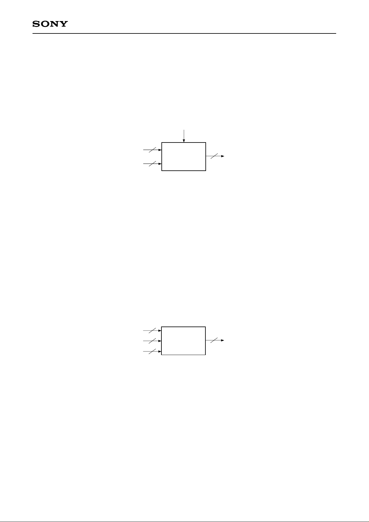
CXD3526GG
(m) Mute 2
This block perfor ms mute processing by replacing the video signal with data of the desired level. The settings
are as follows.
MUTE2_ON: 1 = Mute processing ON, 0 = OFF (Setting shared by R, G and B)
R, G, B_MUTE2: RGB mute data (Set independently for R, G and B)
Processing ON/OFF
10
Input
Coefficient
10
Selector
10
Output
(n) Limiter
This block performs limiter processing so that the output signal does not exceed a certain range. The settings
are as follows.
L_LIM_DAT: Low side limiter level
When input data ≤ L_LIM_DAT, the output is clipped to L_LIM_DAT.
H_LIM_DAT: High side limiter level
When H_LIM_DAT ≤ input data, the output is clipped to H_LIM_DAT.
(Both settings shared by R, G and B)
Set data so that the relationship L_LIM_DAT < H_LIM_DAT is constantly maintained. When both coefficient
values are 000h, limiter processing is not performed.
10
Input
Coefficient (H side)
Coefficient (L side)
10
10
Limiter
10
Ouput
– 49 –
Page 50
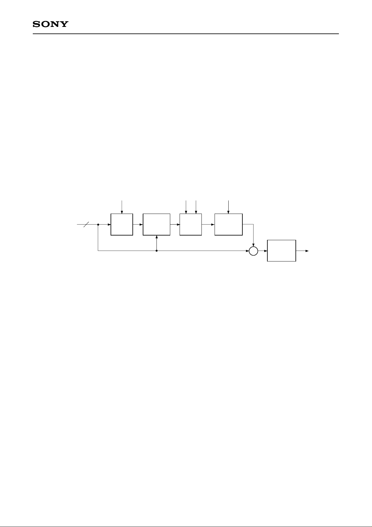
CXD3526GG
(o) Ghost cancel
This block uses signal processing to correct ghosting generated internally within the LCD panel. Correction is
performed by attenuating the video signal and adding after 6 or 12 dots. Equipped with a limiter, the following
settings result in processing only for a video signal of a set level or higher.
GC_ON: 1 = Ghost cancel processing ON; 0 = OFF (Settings shared by R, G and B)
GC_MODE: 1 = 12-dot period processing ON; 0 = 6-dot period processing (Settings shared by R, G and B)
R (G, B)_GC_ATT: 8-bit gain data (Set independently for R, G and B)
The difference between the video signal prior to 6 or 12 dots and the video signal of dots for which processing
is to be performed is found. Attenuation is performed based on this difference and added to the video signal to
correct ghosting. In addition, settings can be made so that a limiter is used to ensure processing is performed
only when the difference in the video signals is of a set level or higher.
Input
10
Level selection
Shift
Register
6 levels or 12 levels
Arithmetic
unit
Coefficient
Limiter
Processing
ON/OFF
Coefficient
Attenuator
–
+
Clip
processing
Output
– 50 –
Page 51

CXD3526GG
(p) Cycle offset
This block performs addition and subtraction processing for port. Arithmetic coefficients are selected
sequentially using the counter output value as the select signal. Therefore, a cyclic offset relative to the video
signal can be attached. The settings are as follows.
OFFSET_ON: 1 = Offset processing ON, 0 = OFF (Setting shared by R, G and B)
OFFSET_MODE: 0 = 6-dot period, 1 = 12-dot period (Setting shared by R, G and B)
R (G, B)_OFFSET1 to 12: 4-bit offset data with code
–8 to +7 graduation, variable with an accuracy of 1 bit
(Set independently for R, G and B)
The counter operation selects offset data sequentially from R (G, B)_OFFSET1. The offset data MSB is the
code bit. Addition is performed when MSB = 0, and subtraction when MSB = 1. However, when performing
subtraction, set the two's complement in the lower bits of the coefficient. When the operation results overflow
or underflow, clipping is performed.
TG block H position
counter reset pulse
Counter
Counter period
Processing ON/OFF
4 4 × 12
Addition/subtraction
10 10
Selector
4
and
clipping
Coefficient (1 to 12)
OutputInput
The counter reset pulse is a reset pulse of TG block H position counter, and that is linked with the HP setting
values set by TG block register. The counter reset timing is delayed by 9 clocks from the front edge of the
HDIN input when HP[10:0] = 000h.
CLK
HDIN
R, G, BOUT
9 clocks
123456123456
HP[10:0] = 000h, 6-dot Period Processed Timing
– 51 –
Page 52
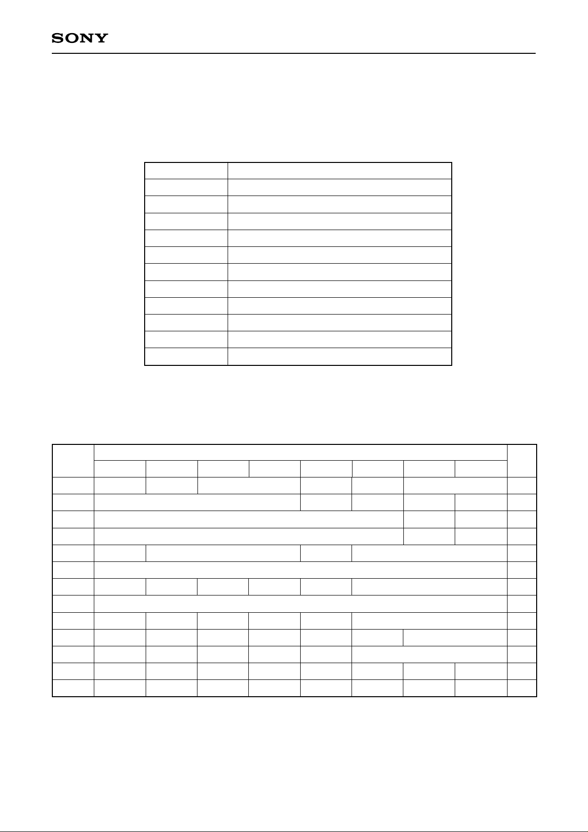
CXD3526GG
6. Register Interface
With this IC, each register and RAM data are set by the host I/F. Addresses for each data are mapped onto a
64K-byte memory space and can be accessed individually. Note that since this is an interface with an external
ROM that mapping of the data area is scattered.
Start address Block name
0000h
1000h
2000h
3000h
4000h
8000h
9000h
A000h
C000h
D000h
E000h
Serial Bus Control Registers
Sub
address
0000h
0001h
0002h
0003h
0004h
0005h
0006h
0007h
0008h
0009h
DATA7
TEST1
—
—
—
—
DA TA6 DATA5 DATA4 DATA3 DATA2 DATA1 DATA0
—
RSLV_ADDR[7:4]
—
—
—
Serial bus control register
TG block
DSD block
Color shading correction block
Pattern generator
RAM for gamma correction block (Red)
RAM for gamma correction block (Green)
RAM for gamma correction block (Blue)
RAM for color shading correction block (Red)
RAM for color shading correction block (Green)
RAM for color shading correction block (Blue)
ROM_MAP[1:0]
GAM_ADDR[15:10]
CSC_ADDR[15:10]
CSC_ADDR[18:16]
—
—
—
Data
ROM_RMOD
—
—
CSC_SIZE[7:0]
—
ROM_TRAN[7:0]
—
—
—
—
—
TEST2
—
ROM_RST
RSCL_SEL[1:0]
—
—
—
GAM_ADDR[18:16]
CSC_SIZE[10:8]
ROM_TRAN[10:8]
REF_MODE[1:0]
Initial
value
00h
—
—
—
00h
00h
00h
00h
00h
00h
00h
00h
00h
000Ah
000Bh
000Ch
—
—
—
—
—
—
—
—
—
—
—
—
—
—
—
RAM_FAIL
—
REF_RSEL[2:0]
—
ROM_FA I L
FORCE_VD
REF_END
00h
00h
00h
—: Don't care
– 52 –
Page 53

The detailed setting contents are described below.
(a) ROM_MAP[1:0] (sub address: 0000h)
This sets the size of the external EEPROM. The values are as follows.
00: 512K bits (65,536 × 8 bits)
01: 256K bits (32,768 × 8 bits)
10: 128K bits (16,384 × 8 bits)
11: 64K bits (8,192 × 8 bits)
(b) ROM_RMOD (sub address: 0000h)
This sets the read access mode of the external EEPROM. Setting values are as follows.
0: Normal mode (Default)
A memory address is always output when read access is performed on external EEPROM.
1: High speed mode
Memory access is performed using the address held by external EEPROM in the case of continuous
read when read access is performed on external EEPROM.
CXD3526GG
(c) RSCL_SEL[1:0] (sub address: 0000h)
The clock output on RSCL is set according to the master clock being used. Setting values are as follows.
00: 35MHz or less
01: 70MHz or less
10: 94.5MHz or less
11: 100MHz or less
(d) TEST1 and TEST2 (sub address: 0000h)
These set the test mode. This is fixed to "0".
(e) RSLV_ADDR[7:4] (sub address: 0001h)
This sets the slave address of the exter nal EEPROM. Although addresses of reserved areas can be set, be
sure to set appropriate addresses. The lower portion of the slave addresses is determined by memory
mapping.
– 53 –
Page 54

CXD3526GG
(f) GAM_ADDR[18:10] (sub addresses: 0002h and 0004h)
This sets the start address ([18:10]) used when storing gamma correction data on the external EEPROM. The
lower address ([9:0]) is fixed to "0" and settings can be made in 1K-byte units.
(g) CSC_ADDR[18:10] (sub addresses: 0003h and 0004h)
This sets the start address ([18:10]) used when storing color shading correction data on the external
EEPROM. The lower address ([9:0]) is fixed to "0" and settings can be made in 1K-byte units.
(h) CSC_SIZE[10:0] (sub addresses: 0005h and 0006h)
This sets "the size of color shading correction data – 1" in 11 bits.
(i) ROM_TRAN[10:0] (sub addresses: 0007h and 0008h)
The lower 11 bits are used to set "the number of bytes – 1" to be transferred per access for the external
EEPROM during refresh and write-back operations.
(j) ROM_RST (sub address: 0009h)
This causes forced reset of the external ROM I/F circuit. A reset is executed when "1" is written to this bit. "0"
is read during read operations.
(k) REF_MODE[1:0] (sub address: 0009h)
This sets the operation settings for the refresh circuit. Setting values are as follows.
00: Refresh stop mode
During refresh stop mode, internal RAM can be accessed by the host.
01: Self-refresh mode
During self-refresh mode, internal RAM cannot be accessed by the host. Refresh starts when ver tical
blanking starts.
10: Forced refresh mode
Used to transfer external EEPROM data to internal RAM at times such as during Power ON. The
external EEPROM address for data to be transferred is determined based on each start address
register. Whether the data being transferred is gamma data or color shading data is determined by
REF_RSEL[2].
Refresh starts when this mode is set.
11: Write-back mode
Internal RAM data is transferred to external EEPROM in order to write data to external EEPROM at
times such as during manufacture. The external EEPROM address of data to be transferred is
determined by each star t address register. Whether the data being transferred is gamma data or color
shading data is determined by REF_RSEL[2].
Write-back starts when this mode is set.
Each of these modes can be executed by writing these bits.
– 54 –
Page 55

CXD3526GG
(l) REF_RSEL[2:0] (sub address: 000Ah)
Sets whether to access the gamma RAM area or color shading RAM area during write-back and refresh
modes. In addition, the area to be accessed automatically changes to the next access area when all transfers
for a given area have been completed.
The order in which area are accessed is: Gamma (Red) → Gamma (Green) → Gamma (Blue) → Color
shading (Red) → Color shading (Green) → Color shading (Blue) → Gamma (Red).
It is possible to read this bit during operations to find out which RAM is currently being accessed. The settings
are as follows.
000: Accesses the Gamma RAM (Red) area.
001: Accesses the Gamma RAM (Green) area.
010: Accesses the Gamma RAM (Blue) area.
011: Reserved
100: Accesses the Color shading RAM (Red) area.
101: Accesses the Color shading RAM (Green) area.
110: Accesses the Color shading RAM (Blue) area.
111: Reserved
(m) FORCE_VD (sub address: 000Bh)
Forcibly generates a VD pulse for writing to double registers. VD is generated when "1" is written to this bit.
"0" is read during read operations.
(n) RAM_FAIL (sub address: 000Ch)
Indicates whether or not accessing internal RAM succeeded. Cleared when "1" is written to this bit.
Status: 0 = Succeeded in accessing internal RAM; 1 = Failed in accessing internal RAM
(o) ROM_FAIL (sub address: 000Ch)
Indicates whether or not accessing external EEPROM succeeded. Cleared when "1" is wr itten to this bit.
Status: 0 = Succeeded in accessing external EEPROM; 1 = Failed in accessing external EEPROM
If the external EEPROM is being written during write-back, ACK is not returned by Ack Polling. This means that
"1" is set for this bit during Ack Polling. However, this bit is automatically cleared when the wr ite operation is
complete and ACK is returned by Ack Polling.
(p) REF_END (sub address: 000Ch)
Indicates that forced refresh or write-back operations are complete. Cleared when "1" is written to this bit.
Status: 1 = Access of external EEPROM is complete
– 55 –
Page 56

TG Block Register
CXD3526GG
Sub
address
1000h
1001h
1002h
1003h
1004h
1005h
1006h
1007h
1008h
1009h
100Ah
100Bh
100Ch
100Dh
100Eh
100Fh
1010h
1011h
1012h
1013h
1014h
1015h
DATA7
—
HSTM
—
—
—
—
POLDET
FRPM[1:0]
PRGU[9:8]
FRPP[9:8]
Data
DA TA6 DATA5 DATA4 DATA3 DATA2 DATA1 DATA0
PSTM
—
—
—
—
HPOL
HSTPOL
HSTFIX
—
—
PRGD[9:8]
VPOL
HCKPOL
HCKFIX
VFRRN[10:3]
—
PLLP[7:0]
—
HP[7:0]
VP[7:0]
PRGU[7:0]
PRGD[7:0]
SHSTU[7:0]
SHSTD[7:0]
HD1U[10:8]
FRPP[7:0]
HD1U[7:0]
HD1D[7:0]
CLPU[10:8]
CLPU[7:0]
CLPD[7:0]
HR
VSTPOL
VSTFIX
—
—
SHSTU[9:8]
SHP[5:0]
RGT
VCKPOL
VCKFIX
DWN
DCKPOL
DCKFIX
PLLP[10:8]
HP[10:8]
SHSTD[9:8]
HD1D[10:8]
CLPD[10:8]
FRVCLNK
PSTPOL
DCKFINV
Initial
value
30h
FFh
FFh
FFh
00h
00h
00h
00h
00h
00h
00h
00h
00h
00h
00h
00h
00h
00h
00h
00h
00h
00h
1016h
1017h
1018h
1019h
101Ah
101Bh
101Ch
101Dh
101Eh
101Fh
1020h
1021h
1022h
1023h
—
—
—
—
—
PCGU[9:8]
CLRU[9:8]
—
—
—
—
—
DCKF[3:0] DCKW[3:0]
PCGD[9:8]
PCGU[7:0]
PCGD[7:0]
ENBU[7:0]
ENBD[7:0]
CLRD[9:8]
CLRU[7:0]
CLRD[7:0]
HSTPC[5:0]
HSTPF[5:0]
PSTPC[5:0]
PSTPF[5:0]
HCKC[5:0]
ENBU[9:8]
VCKP[9:8]
– 56 –
ENBD[9:8]
VSTP[10:9]
00h
00h
00h
00h
00h
00h
00h
00h
00h
00h
00h
00h
00h
00h
Page 57

CXD3526GG
Sub
address
1024h
1025h
1026h
1027h
1028h
1029h
102Ah
102Bh
102Ch
102Dh
DATA7
—
PO2
CLKOUT
HSTOE
Data
DA TA6 DATA5 DATA4 DATA3 DATA2 DATA1 DATA0
VCKP[7:0]
VSTP[8:1]
—
PO1
HD1OE
PSTOE
CLPOE
HCKOE
HD2U[10:8]
HD2U[7:0]
HD2D[7:0]
HD3U[10:8]
HD3U[7:0]
HD3D[7:0]
PRGOE
DCKOE
SHSTOE
VOE
FRPOE
PCGOE
HD2D[10:8]
HD3D[10:8]
XFRPOE
HD3OE
HD2OE
CLROE
—: Don't care
Initial
value
00h
00h
00h
00h
00h
00h
00h
00h
00h
00h
– 57 –
Page 58
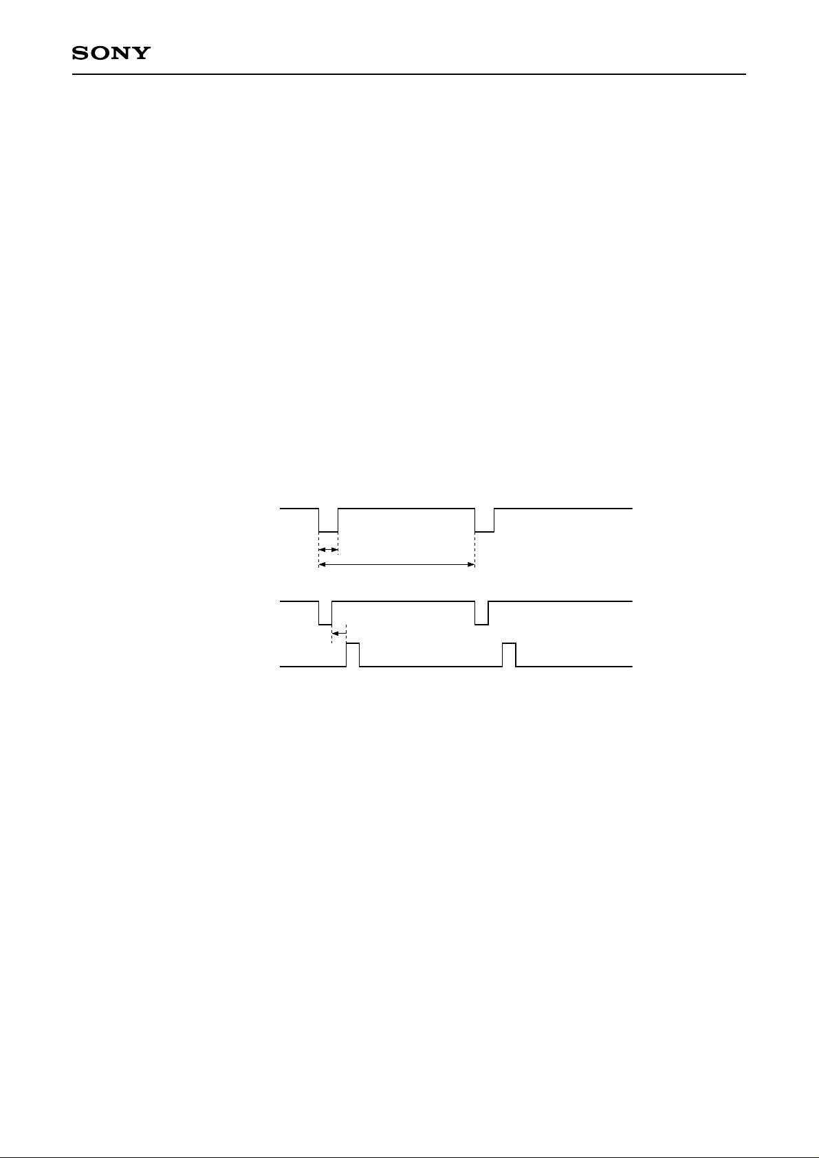
CXD3526GG
The detailed setting contents are described below.
(a) Clock settings
(1) CLKOUT (sub address: 102Ch)
This sets the Pin 28 clock output.
Setting value: 1 = Internal clock is inve r ted and output, 0 = Low is output
(b) SYNC polarity settings
(1) POLDET (sub address: 1000h)
This sets the sync polarity auto discrimination function ON/OFF.
Setting value: 1 = Auto discrimination function ON, 0 = Auto discrimination function OFF
When POLDET = 1, the HPOL and VPOL settings below are invalid. When using this function, the HDIN sync
portion must be 1/2 or less of 1H, and the VDIN sync portion must come before the rise position of the VST
pulse.
HDIN (Negative)
N/2 or less
N
VDIN (Negative)
Must come before VST
VST
(2) HPOL and VPOL (sub address: 1000h)
These set the sync signal polarity when POLDET = 0.
Setting value: 1 = Positive polar ity, 0 = Negative polarity
The internal operation of this IC is with the input sync signal fixed to positive polarity. Therefore, these HPOL
and VPOL must be set in accordance with the polarity of the sync signal input from HDIN and VDIN.
Set HPOL and VPOL to "1" when the input sync signal is positive polar ity, or to "0" when negative polar ity.
– 58 –
Page 59

CXD3526GG
(c) Dots per 1H and lines per 1V settings
(1) HR (sub address: 1000h)
This sets the PLL counter reset ON/OFF.
Setting value: 1 = Reset enabled, 0 = Reset disabled
When HR = 0, the internal frequency divider is used, and the HD1 pulse output should be used as the return
pulse. The number of dot clocks per 1H is set by PLLP[11:1] below.
(2) PLLP[10:0] (sub addresses: 1004h and 1005h)
This sets the internal PLL counter reset period in 11 bits. Setting is possible in 1-dot units.
When HR = 0, free-running occurs at the above N. When HR = 1, if the next HDIN is not input before the
internal PLL counter counts up to 2047, free-running mode is established and free-running occurs at N.
When HDIN is input, free-running is canceled and normal operation is established.
(3) VFRRN[10:3] (sub address: 1003h)
This sets the number of lines in 9 bits during vertical free running. Setting is possible in 4-line units. To have
operation run freely at M lines, set the "(M – 4)/4" value. If the next VDIN is not input before the internal vertical
line counter counts up to 2047, free-running mode is established. When VDIN is input, free-running is canceled
and normal operation is established.
(d) Scan direction settings
RGT and DWN (sub address: 1000h)
These settings switch the scan directions of the LCD panel.
Setting value: 1 = Forward scan, 0 = Reverse scan
When CTRL (Pin 88) is low, RGT (Pin 2) and DWN (Pin 49) function as output pins, and the data set in the
respective registers is reflected. When CTRL is high, this setting is ignored, RGT and DWN function as input
pins, and are reflected to internal operation.
(e) PO1 and PO2 output settings
PO1 and PO2 (sub address: 1029h)
These set the PO1 and PO2 output.
Setting value: 1 = High is output, 0 = Low is output
The set data is reflected to the output pins PO1 (Pin 47) and PO2 (Pin 48) of the same name.
– 59 –
Page 60
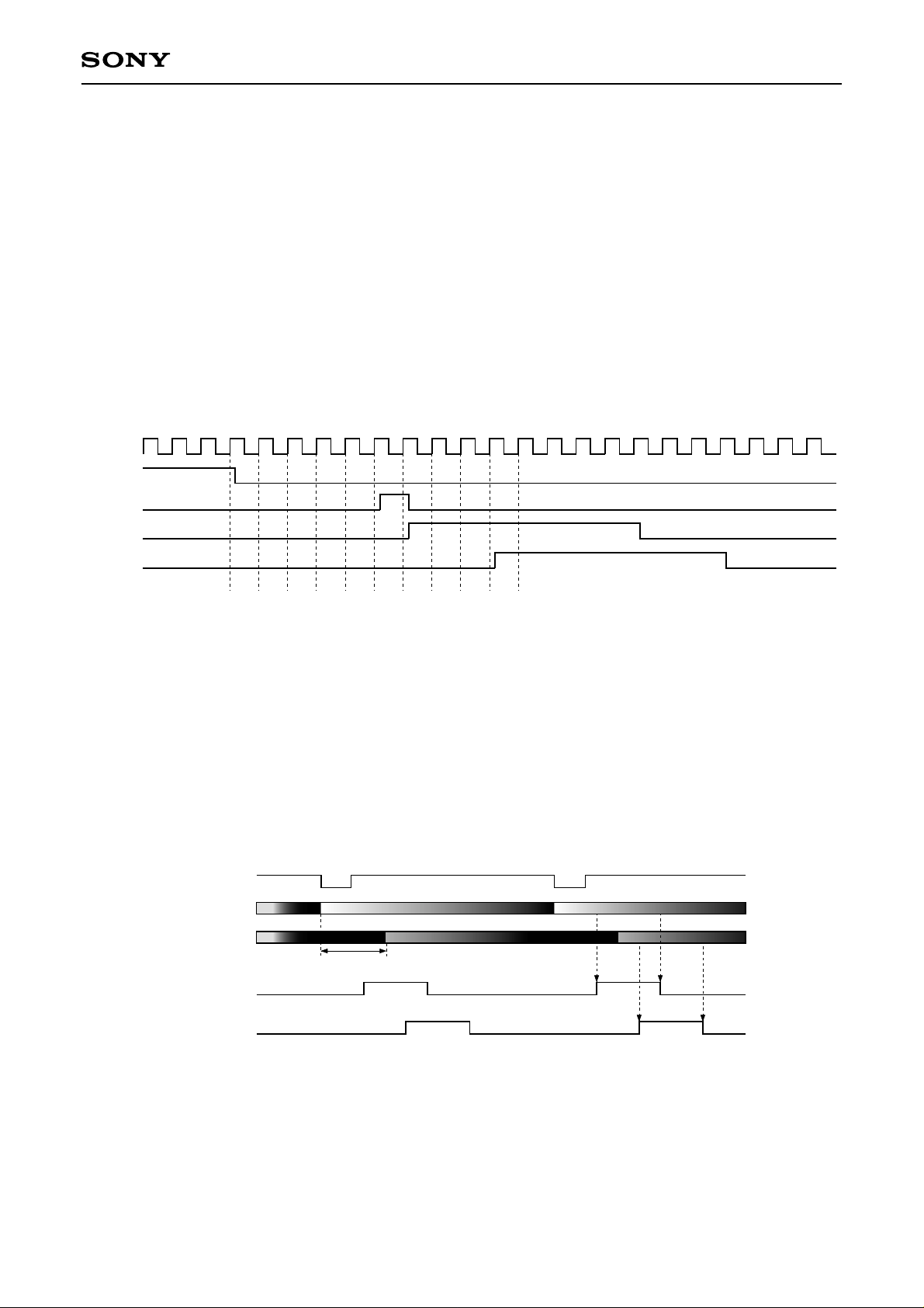
CXD3526GG
(f) Horizontal display position and horizontal direction pulse settings
(1) HP[10:0] (sub addresses: 006h and 007h)
HP[10:0] sets the horizontal pulse position for the LCD panel in 11 bits. The position can be set in 1-dot units
using the internal pulse INT_HD generated from the front edge of HDIN as the reference. The HP setting range
is from "0 to (N – 1)".
If the HP value is set to the number of frequency divisions N or higher, the HP setting is ignored and "(N – 1)"
is used as the setting value.
The HST‚ PST, HCK1, HCK2, DCK1, DCK2, ENB, VST, VCK, FRP, XFRP, PCG, BLK, HD2 and HD3 horizontal
timing pulses are linked according to the HP setting.
The internal reference pulse INT_HD rises at the 5th clock from the front edge of the HDIN input, and all the
pulses are synchronized using this as the reference. Increasing HP shifts the output positions of the linked
pulses toward the rear of the time series. The example below shows the shortest output position from HDIN
when HP is set to 000h. (Note that the output position changes according to the settings in (2) below.)
CLK
HDIN
INT_HD
HD1
HD2
(2) CLPU[10:0], CLPD[10:0], PRGU[9:0], PRGD[9:0], HD1U[10:0], HD1D[10:0], SHSTU[9:0], SHSTD[9:0],
PCGU[9:0], PCGD[9:0], ENBU[9:0], ENBD[9:0], HD2U[10:0], HD2D[10:0], HD3U[10:0] and HD3D[10:0]
(sub addresses: 1009h to 100Eh, 1010h to 1014h, 01Ch to 020h and 1026h to 102Bh)
These set the horizontal timing pulse output positions in 10 bits or 11 bits. The respective rise and fall positions
can be set in 1-dot units. Settings ending in "U" set the rise position, and settings ending in "D" set the fall
position. Horizontal pulses are divided into the following two types.
(A) CLP and HD1 → Pulses synchronized to the PLL counter
Set the "rise position/fall position – 5" value.
(B) PRG, SHST, PCG, ENB, HD2 and HD3 → Pulses synchronized to the HP counter
Set the "rise position/fall position – HP setting value – 8" value.
An outline of each type is shown below. When ∗∗U and ∗∗D are set to the same value, "1" is output.
HDIN
PLL counter
HP counter
(A)
0
HP[10:0]
0
0
0
∗
U
∗
D
(B)
∗
U
∗
D
(3) HD1OE, HD2OE, HD3OE, CLPOE, PRGOE, SHSTOE, PCGOE and CLROE
(sub addresses: 102Ch and 102Dh)
These set the output limit of HD1, HD2, HD3, CLP, PRG, SHST, PCG and CLR pulses, respectively.
Setting value: 1 = Pulse is output, 0 = Output is fixed to "0"
– 60 –
Page 61
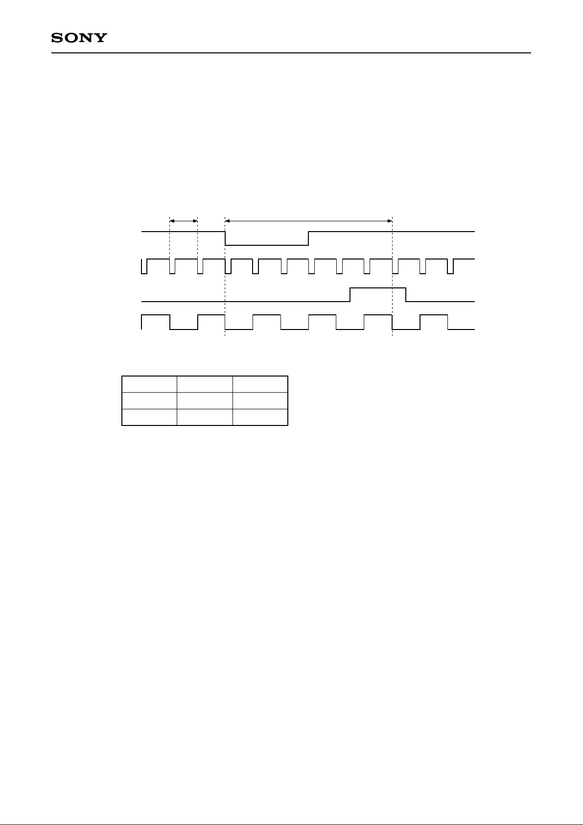
CXD3526GG
(g) Vertical display position setting
VP[7:0] (sub address: 1008h)
This sets the vertical display start position in 8 bits. The position can be set in 1-line units using the front edge
of VDIN as the reference. The VST, VCK, FRP and XFRP pulse phases change by linking with this setting.
Minimum
adjustment
width: 1H
VDIN
HDIN
VST
VCK
Tvp
Tvp minimum and maximum setting values
VP[7:0]
Tvp
Min.
000h
6H
Max.
FFh
261H
– 61 –
Page 62
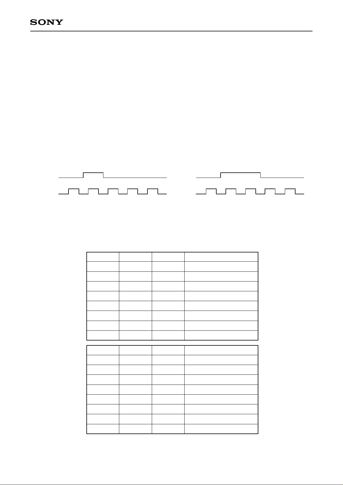
(h) HST and PST pulse settings
(1) HSTM (sub address: 1002h)
This sets the pulse width for horizontal display start timing pulse HST.
Setting value: 1 = Twice the HCK period width, 0 = HCK per iod width
Set the width according to the LCD panel specifications.
(2) PSTM (sub address: 1002h)
This sets the pulse width for dot sequential precharge start timing pulse PST.
Setting value: 1 = Twice the HCK period width, 0 = HCK per iod width
Set the width according to the LCD panel specifications.
CXD3526GG
HST, PST
HCK1
HSTM, PSTM = 0
HST, PST
HCK1
HSTM, PSTM = 1
(3) HSTFIX, HSTPOL and PSTPOL (sub addresses: 1001h and 1002h)
These set the HST and PST pulse output polarities. The polarity changes as follows according to the combination
of linked/not linked with control signal RGT.
HSTFIX
0
0
0
0
1
1
1
HSTPOL
0
0
1
1
0
0
1
RGT
0
1
0
1
0
1
0
HST pulse output polarity
Positive
Negative
Negative
Positive
Negative
Negative
Positive
1
HSTFIX
0
0
0
0
1
1
1
1
1
PSTPOL
0
0
1
1
0
0
1
1
1
RGT
0
1
0
1
0
1
0
1
– 62 –
Positive
PST pulse output polarity
Positive
Negative
Negative
Positive
Negative
Negative
Positive
Positive
Page 63
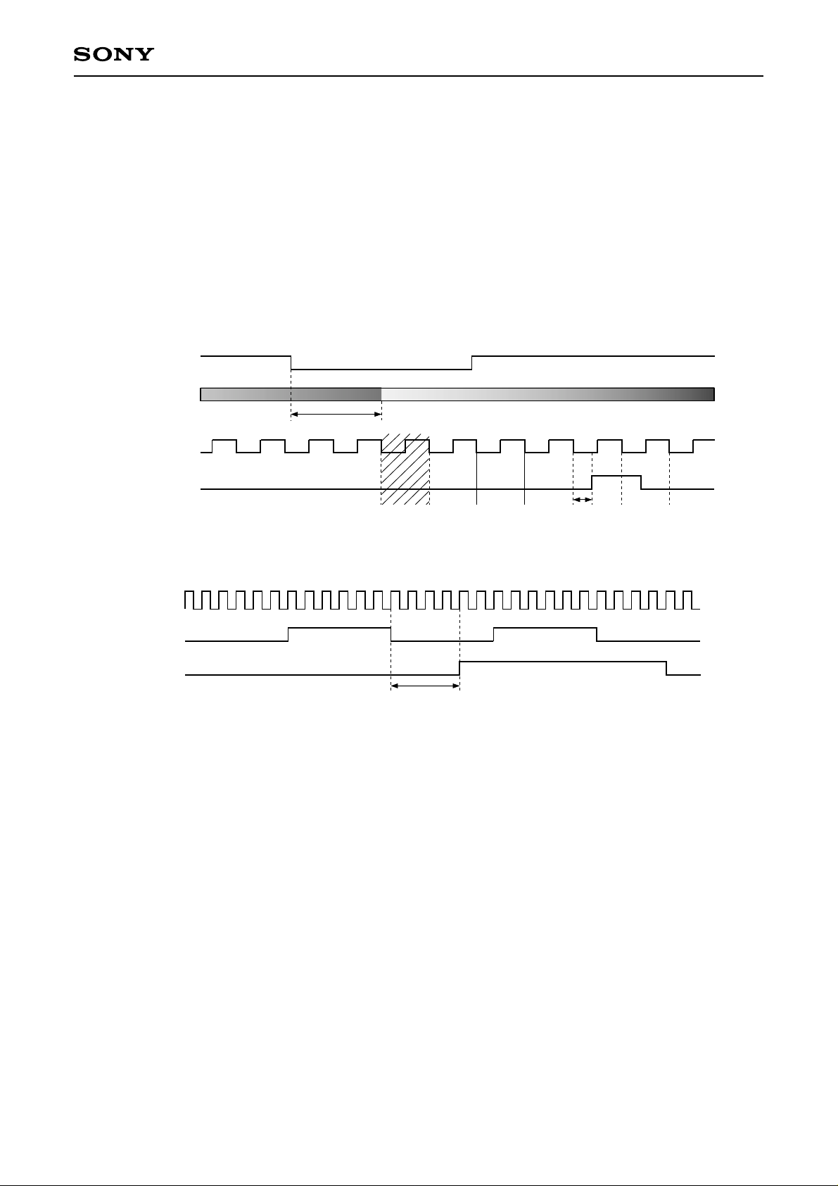
CXD3526GG
(4) HSTPC[5:0], HSTPF[5:0], PSTPC[5:0] and PSTPF[5:0] (sub addresses: 1016h to 1019h)
These set the HST and PST pulse phases. Reset is applied when the internal HP counter reaches "0", and the
HST and PST pulse phases within 1H can be set at the HCK1 and HCK2 period, respectively, by HSTPC and
PSTPC.
HSTPF and PSTPF can set the HST and PST pulse phase relative to HCK1 and HCK2 in 1-dot units.
Do not set HSTPC and PSTPC to 00h, as the pulses may not be output correctly in this case.
The HSTPF and PSTPF values can be set up to "(HCKC × 2 – 2)". If higher values are set, the pulses are not
output. Set the "(phase difference from HCK pulse)" value.
The figures below show the timings for HSTPC: 04h and HSTPF: 04h, respectively. These timings are the
same for the PST pulse.
HDIN
0
HP counter
HP[10:0]
HCK1
10 23456
HST
Setting prohibited HSTPF[5:0]
CLK
HCK1
HST
HSTPF = 04h
(5) HSTOE and PSTOE (sub address: 102Dh)
These set the output limit of HST and PST pulses output limits, respectively.
Setting value: 1 = Pulse is output, 0 = Output is fixed to "0"
– 63 –
Page 64

CXD3526GG
(i) HCK1 and HCK2 pulse settings
(1) HCKC[5:0] (sub address: 101Ah)
This sets the HCK1 and HCK2 period (LCD panel sampling period). Settings which result in an odd number for
Tckw in the figure below are prohibited, so be sure to set a value that results in an even number. Set the
"(Tckw – 1)" value according to the LCD panel specifications. When this setting is changed, the HST and PST
pulse phases also change, so first set HCKC to the correct value and then make the HST and PST settings.
Example setting values are shown in the table below.
CLK
HCK1
LCD panel
SVGA
XGA, WXGA
Tckw
12 clk
24 clk
Tckw
HCKC
0Bh
17h
(2) HCKFIX and HCKPOL (sub addresses: 1002h and 1001h)
These set the HCK1 and HCK2 pulse output polarity. The polarity relative to the HST pulse changes as follows
according to the combination of linked/not linked with control signal RGT.
HCKFIX
0
0
0
0
HCKPOL
0
0
1
1
RGT
0
1
0
1
Output polarity
Positive
Negative
Negative
Positive
1
1
1
1
Positive
HST
HCK1
0
0
1
1
0
1
0
1
HST
HCK1
(3) HCKOE (sub address: 102Dh)
This sets the output limit of HCK1 and HCK2 pulses output limits.
Setting value: 1 = Pulse is output, 0 = Output is fixed to "0"
– 64 –
Negative
Negative
Positive
Positive
Negative
HSTPF[5:0] = 00hHSTPF[5:0] = 00h
Page 65
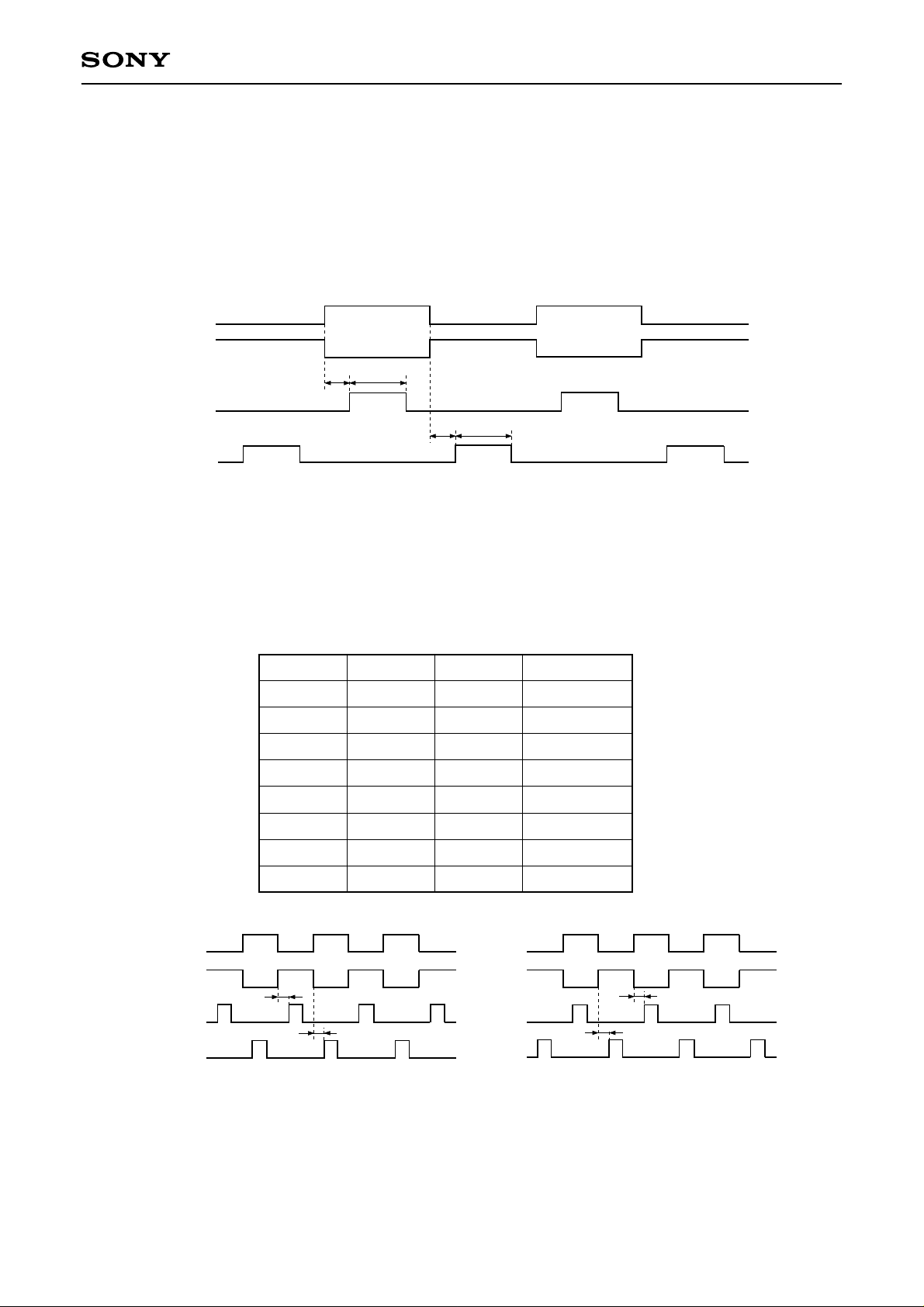
CXD3526GG
(j) DCK1 and DCK2 pulse settings
(1) DCKF[3:0] and DCKW[3:0] (sub address: 101Bh)
These set the DCK1 and DCK2 pulse phases and widths. DCKF sets the DCK1 and DCK2 pulse phases
relative to HCK in 0.5-dot units. Set the "Tdckf" value.
The DCKFINV, DCKFIX and RGT settings differ according to whether the phase is synchronized with the rising
edge of HCK1 or HCK2.
The DCK1 and DCK2 pulse width can be set in 1-dot units by DCKW. Set the "Tdckw – 1" value.
HCK1
HCK2
Tdckf
DCK1
DCK2
Tdckw
Tdckf
Tdckw
(2) DCKPOL (sub address: 1001h)
This setting switches the DCK1 and DCK2 pulse output polarities.
(3) DCKFINV and DCKFIX (sub address: 1002h)
This setting switches the DCK1 and DCK2 output phases relative to HCK1 and HCK2. The output phase is as
follows by setting right/left inversion control signal RGT.
DCKFIX
0
0
0
0
1
1
1
1
HCK1
HCK2
A
DCKFINV
0
0
1
1
0
0
1
1
RGT
0
1
0
1
0
1
0
1
Output phase
A
B
B
A
B
B
A
A
B
HCK1
HCK2
DCK1
DCK2
(4) DCKOE (sub address: 102Dh)
This sets the output limit of DCK1 and DCK2 pulses.
Setting value: 1 = Pulses are output, 0 = Output is fixed to "0"
– 65 –
DCK1
DCK2
Page 66
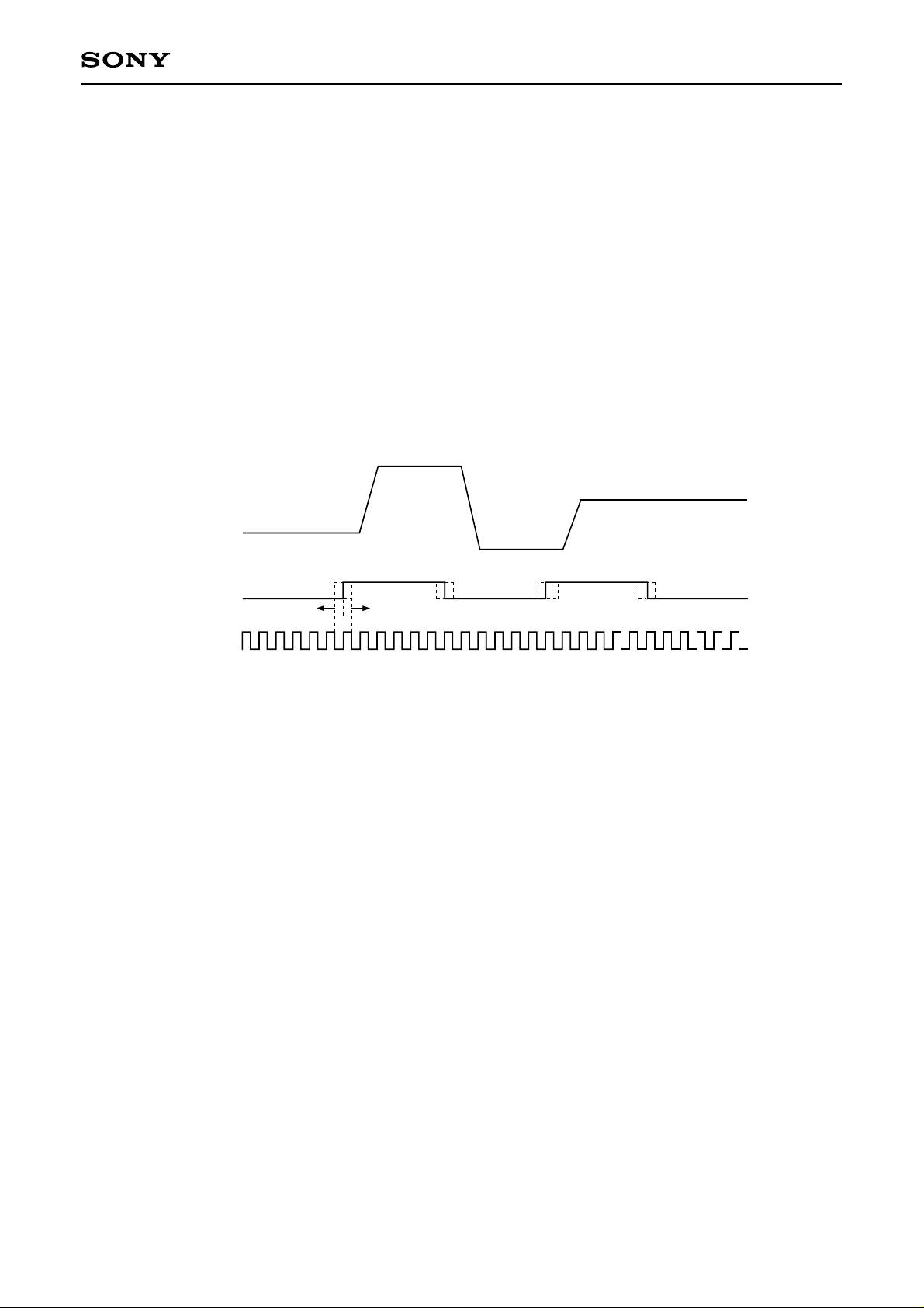
CXD3526GG
(k) LCD panel sample-and-hold position setting
SHP[5:0] (sub address: 1015h)
This sets the horizontal transfer start pulse and clock pulse phases relative to the video signal to the LCD
panel. The phase can be set in 64 positions with 6 bits. Incrementing SHP by +1 shifts the HST, PST, HCK1,
HCK2, DCK1 and DCK2 pulses forward by 0.5 dot (half the internal clock period). The LCD panel sample-andhold position can be set by shifting the above pulse phases forward or backward relative to the video signal. At
this time, the phases between the HST, PST, HCK1, HCK2, DCK1 and DCK2 pulses do not change. The figure
below shows an example of HCK1 during 12-dot simultaneous sampling.
This setting eliminates the need to set the sample-and-hold position with a Sony sample-and-hold driver IC,
and makes it possible to adjust the phases of the video signal to the LCD panel and the horizontal transfer
clock without changing the position of the video signal on the screen.
Video signal to
LCD panel
HCK1
CLK
SHP increased
SHP decreased
– 66 –
Page 67

CXD3526GG
(l) VST and VCK pulse settings
(1) VSTP[10:1] (sub addresses: 1021h and 1025h)
This sets the VST pulse rise and fall positions within 1H in 10 bits. The positions can be set in 2-dot units using
the internal HP counter "0" position as the reference. Set the "(Tvstp – 2)/2" value.
HDIN
HP counter
VST
VCK
0
Tvstp
Tvckp
(2) VCKP[9:0] (sub addresses: 1021h and 1024h)
This sets the VCK, FRP and XFRP inversion positions within 1H in 10 bits. The positions can be set in 1-dot
units using the internal HP counter "0" position as the reference. Set the "Tvckp – 1" value.
(3) VSTFIX and VCKFIX (sub address: 1002h), VSTPOL and VCKPOL (sub address: 1001h)
These set the VST and VCK pulse output polarities. The VST pulse polarity and the VCK pulse polarity relative
to the VST pulse change as follows according to the combination of linked/not linked with control signal DWN.
∗∗∗
FIX
0
0
0
0
1
1
1
1
∗∗∗
POL
0
0
1
1
0
0
1
1
DWN
0
1
0
1
0
1
0
1
Output polarity
Positive
Negative
Negative
Positive
Negative
Negative
Positive
Positive
∗∗∗
: VST or VCK
(4) VOE (sub address: 102Dh)
This sets the output limit of VST, VCK and ENB pulses.
Setting value: 1 = Pulse is output, 0 = Output is fixed to "0"
– 67 –
Page 68
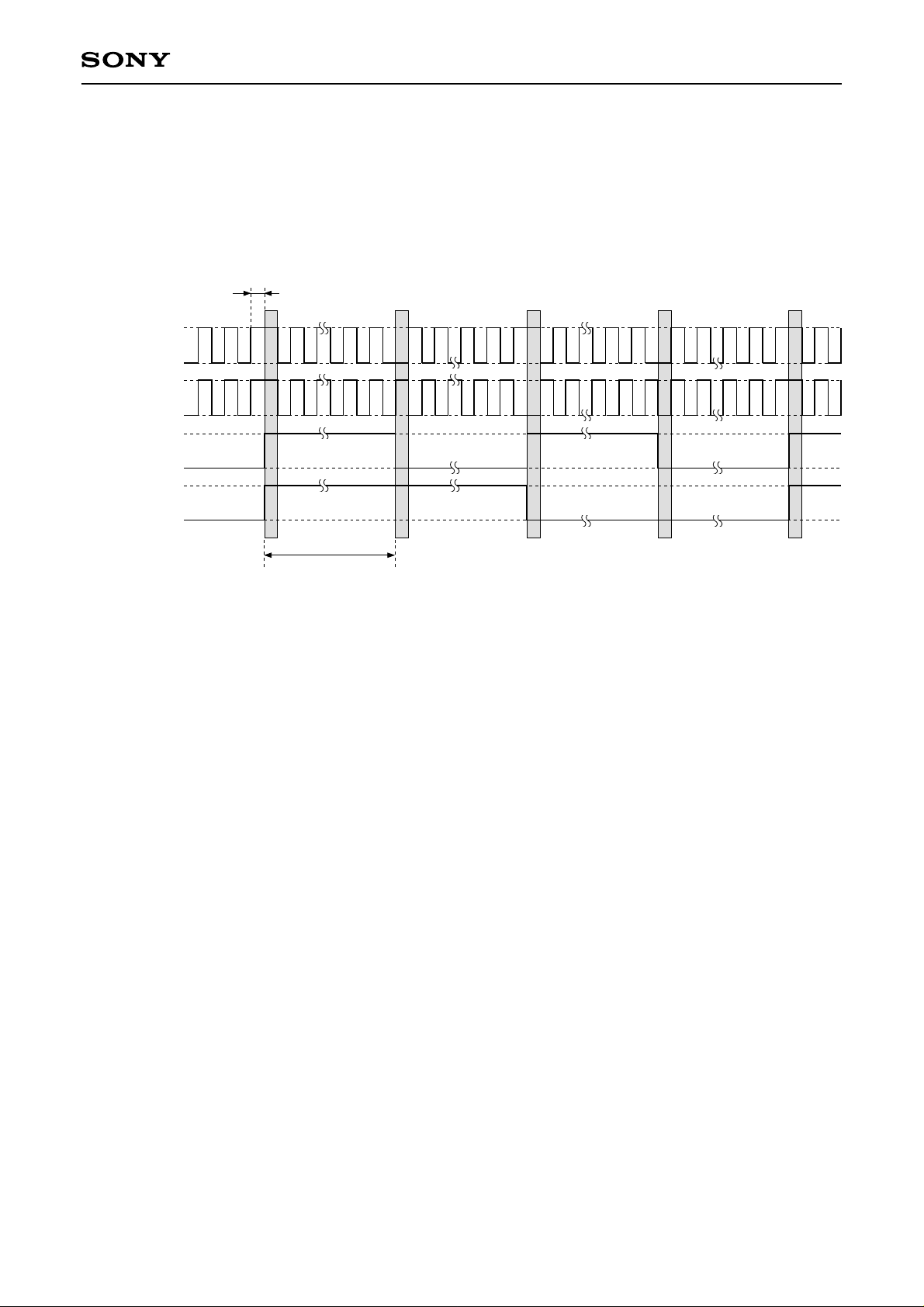
CXD3526GG
(m) FRP and XFRP pulse settings
(1) FRPM[1:0] (sub address: 1001h)
This sets the period for switching the LCD AC conversion signal FRP pulse. 1F/1H, 2F/1H, 1F and 2F inversion
can be set as shown in the figure below. Normally use FRPM: 11.
1H
FRPM: 11
(1F/1H inversion)
FRPM: 01
(2F/1H inversion)
FRPM: 10
(1F inversion)
FRPM: 00
(2F inversion)
1F
(2) FRPP[9:0] (sub addresses: 100Eh and 100Fh)
This sets the FRP and XFRP inversion positions within 1H in 10 bits. The positions can be set in 1-dot
units using the internal HP counter "0" position as the reference. Set the "FRP inversion position – HP
counter "0" position – 1" value.
XFRP is output as the polarity inverted FRP pulse.
(3) FRPOE and XFRPOE (sub address: 102Ch)
These set the output limit of FRP and XFRP pulses, respectively.
Setting value: 1 = Pulse is output, 0 = Output is fixed to "0"
– 68 –
Page 69

CXD3526GG
(n) VCK and FRP transition point shared setting and V block pulse right/left inversion link setting
FRVCLNK (sub address: 1000h)
This sets the VCK pulse transition point.
Setting value: 1 = FRP and VCK transition points are shared,
0 = FRP and VCK transition points are independent
When FRVCLNK = 1, the VCK inversion timing is forcibly synchronized with the FRP inversion timing.
When FRVCLNK = 0, the VCK transition point is independent of FRP.
VCK
FRVCLNK = 1
FRP
FRPP
FRVCLNK = 0
VCK
VCKP
FRP
FRPP
– 69 –
Page 70

DSD Register
CXD3526GG
Sub
address
2000h
2001h
2002h
2003h
2004h
2005h
2006h
2007h
2008h
2009h
200Ah
200Bh
200Ch
200Dh
200Eh
DATA7
—
—
—
—
—
Data
DA TA6 DATA5 DATA4 DATA3 DATA2 DATA1 DATA0
OFFSET_ON—GC_ON
—
R_SUB_BRT[10:8]
B_SUB_BRT[10:8]
FRM_H2[10:8]
LIM_ON—MUTE2_ON
—
USR_GAIN[7:0]
USR_BRT[7:0]
R_SUB_GAIN[7:0]
G_SUB_GAIN[7:0]
B_SUB_GAIN[7:0]
R_SUB_BRT[7:0]
G_SUB_BRT[7:0]
B_SUB_BRT[7:0]
—
—
FRM_H1[7:0]
FRM_H2[7:0]
—
GAM_ON
OFFSET_MODE
USR_BRT[10:8]
G_SUB_BRT[10:8]
FRM_H1[10:8]
MUTE1_ON
GC_MODE
GAM_MODE
FRM_ON
Initial
value
00h
00h
00h
00h
00h
00h
00h
00h
00h
00h
00h
00h
00h
00h
00h
200Fh
2010h
2011h
2012h
2013h
2014h
2015h
2016h
2017h
2018h
2019h
201Ah
201Bh
201Ch
201Dh
201Eh
201Fh
2020h
—
FRM_DAT[9:8]
R_OSD_DAT4[9:8]
G_OSD_DAT4[9:8]
FRM_V2[10:8]
B_MUTE1[9:8]
R_OSD_DAT3[9:8]
G_OSD_DAT3[9:8]
FRM_V1[7:0]
FRM_V2[7:0]
—
FRM_DAT[7:0]
R_MUTE1[7:0]
G_MUTE1[7:0]
B_MUTE1[7:0]
G_MUTE1[9:8]
R_OSD_DAT1[7:0]
R_OSD_DAT2[7:0]
R_OSD_DAT3[7:0]
R_OSD_DAT4[7:0]
R_OSD_DAT2[9:8]
G_OSD_DAT1[7:0]
G_OSD_DAT2[7:0]
G_OSD_DAT3[7:0]
G_OSD_DAT4[7:0]
G_OSD_DAT2[9:8]
FRM_V1[10:8]
R_MUTE1[9:8]
R_OSD_DAT1[9:8]
G_OSD_DAT1[9:8]
00h
00h
00h
00h
00h
00h
00h
00h
00h
00h
00h
00h
00h
00h
00h
00h
00h
00h
2021h
2022h
2023h
B_OSD_DAT1[7:0]
B_OSD_DAT2[7:0]
B_OSD_DAT3[7:0]
– 70 –
00h
00h
00h
Page 71

CXD3526GG
Sub
address
2024h
2025h
2026h
2027h
2028h
2029h
202Ah
202Bh
202Ch
202Dh
202Eh
202Fh
2030h
2031h
2032h
Data
DATA7
B_OSD_DAT4[9:8] B_OSD_DAT3[9:8] B_OSD_DAT2[9:8] B_OSD_DAT1[9:8]
—
—
—
DA TA6 DATA5 DATA4 DATA3 DATA2 DATA1 DATA0
B_OSD_DAT4[7:0]
GAM_H1[7:0]
GAM_H2[7:0]
GAM_H2[10:8]
GAM_V2[10:8]
G_GAM_BRT[10:8]
—
GAM_V1[7:0]
GAM_V2[7:0]
—
R_GAM_GAIN[7:0]
G_GAM_GAIN[7:0]
B_GAM_GAIN[7:0]
R_GAM_BRT[7:0]
G_GAM_BRT[7:0]
B_GAM_BRT[7:0]
—
GAM_H1[10:8]
GAM_V1[10:8]
R_GAM_BRT[10:8]
Initial
value
00h
00h
00h
00h
00h
00h
00h
00h
00h
00h
00h
00h
00h
00h
00h
2033h
2034h
2035h
2036h
2037h
2038h
2039h
203Ah
203Bh
203Ch
203Dh
203Eh
203Fh
2040h
2041h
2042h
2043h
2044h
2045h
2046h
2047h
2048h
—
L_LIM_DAT[9:8]
H_LIM_DAT[9:8]
R_OFFSET2[3:0]
R_OFFSET4[3:0]
R_OFFSET6[3:0]
R_OFFSET8[3:0]
R_OFFSET10[3:0]
R_OFFSET12[3:0]
G_OFFSET2[3:0]
G_OFFSET4[3:0]
———
R_MUTE2[7:0]
G_MUTE2[7:0]
B_MUTE2[7:0]
B_MUTE2[9:8]
L_LIM_DAT[7:0]
H_LIM_DAT[7:0]
B_GC_LIM_DAT[9:8]
R_GC_LIM_DAT[7:0]
G_GC_LIM_DAT[7:0]
B_GC_LIM_DAT[7:0]
R_GC_ATT[7:0]
G_GC_ATT[7:0]
B_GC_ATT[7:0]
—
G_MUTE2[9:8]
G_GC_LIM_DAT[9:8]
R_OFFSET1[3:0]
R_OFFSET3[3:0]
R_OFFSET5[3:0]
R_OFFSET7[3:0]
R_OFFSET9[3:0]
R_OFFSET11[3:0]
G_OFFSET1[3:0]
G_OFFSET3[3:0]
B_GAM_BRT[10:8]
R_MUTE2[9:8]
R_GC_LIM_DAT[9:8]
00h
00h
00h
00h
00h
00h
00h
00h
00h
00h
00h
00h
00h
00h
00h
00h
00h
00h
00h
00h
00h
00h
– 71 –
Page 72
CXD3526GG
Sub
address
2049h
204Ah
204Bh
204Ch
204Dh
204Eh
204Fh
2050h
2051h
2052h
DATA7
Data
DA TA6 DATA5 DATA4 DATA3 DATA2 DATA1 DATA0
G_OFFSET6[3:0]
G_OFFSET8[3:0]
G_OFFSET10[3:0]
G_OFFSET12[3:0]
B_OFFSET2[3:0]
B_OFFSET4[3:0]
B_OFFSET6[3:0]
B_OFFSET8[3:0]
B_OFFSET10[3:0]
B_OFFSET12[3:0]
G_OFFSET5[3:0]
G_OFFSET7[3:0]
G_OFFSET9[3:0]
G_OFFSET11[3:0]
B_OFFSET1[3:0]
B_OFFSET3[3:0]
B_OFFSET5[3:0]
B_OFFSET7[3:0]
B_OFFSET9[3:0]
B_OFFSET11[3:0]
—: Don't care
Initial
value
00h
00h
00h
00h
00h
00h
00h
00h
00h
00h
– 72 –
Page 73
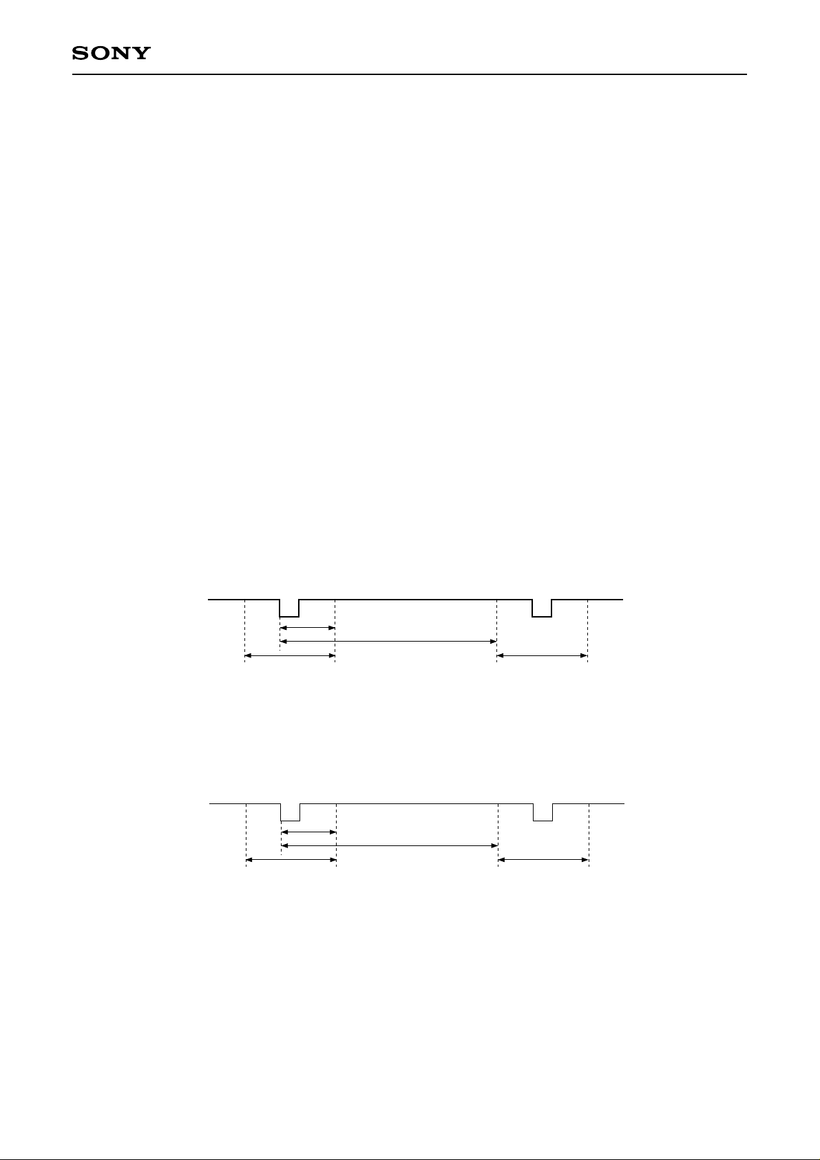
CXD3526GG
The detailed setting contents of DSD are described below.
(a) USR_GAIN[7:0] (sub address: 2002h)
This sets the user adjustment gain block arithmetic coefficients in 8 bits.
(b) USR_BRT[10:0] (sub addresses: 2003h and 200Ah)
This sets the user adjustment bright block arithmetic coefficients in 11 bits with code.
(c) R_SUB_GAIN[7:0], G_SUB_GAIN[7:0] and B_SUB_GAIN[7:0] (sub addresses: 2004h to 2006h)
These set the sub gain block arithmetic coefficients for the R, G and B white balance adjustment in 8 bits.
(d) R_SUB_BRT[10:0], G_SUB_BRT[10:0] and B_SUB_BRT[10:0] (sub addresses: 2007h to 200Bh)
These set the sub bright block arithmetic coefficients for the R, G and B white balance adjustment in 11 bits
with code.
(e) FRM_H1[10:0] and FRM_H2[10:0] (sub addresses: 200Ch to 200Eh)
These set the horizontal black frame display range for the black frame block in 11 bits. The range can be set in
1-dot units. Set the "display range – 2" value.
HDIN
FRM_H2
FRM_H1
Black frame display range Black frame display range
(f) FRM_V1[10:0] and FRM_V2[10:0] (sub addresses: 200Fh to 2011h)
These set the vertical black frame display range for the black frame block in 11 bits. The range can be set in
1-line units. Set the "display range – 2" value.
VDIN
FRM_V2
FRM_V1
Black frame display range Black frame display range
(g) FRM_ON (sub address: 2000h)
This sets the processing ON/OFF for the black frame block.
Setting value: 1 = Black frame processing ON, 0 = Black frame processing OFF
– 73 –
Page 74

(h) FRM_DAT[9:0] (sub addresses: 2012h and 2016h)
This sets the data for the black frame processing block in 10 bits.
(i) MUTE1_ON (sub address: 2000h)
This sets the mute 1 block processing ON/OFF.
Setting value: 1 = Mute 1 processing ON, 0 = Mute 1 processing OFF
(j) R_MUTE1[9:0], G_MUTE1[9:0] and B_MUTE1[9:0] (sub addresses: 2013h to 2016h)
These set the R, G and B mute 1 block data in 10 bits.
(k) R_OSD_DAT1 to 4[9:0], G_OSD_DAT1 to 4[9:0] and B_OSD_DAT1 to 4[9:0]
(sub addresses: 2017h to 2025h)
These set the OSD block signal gradual level of R, G and B in 10 bits.
CXD3526GG
(l) GAM_ON (sub address: 2000h)
This sets the gamma correction block processing ON/OFF.
Setting value: 1 = Gamma correction processing ON, 0 = Gamma correction processing OFF
(m) GAM_MODE (sub address: 2001h)
This sets the gamma correction block RAM operation.
Setting value: 1 = Normal operation mode, 0 = Power-saving mode
(n) GAM_H1[10:0] and GAM_H2[10:0] (sub addresses: 2026h to 2028h)
These set the horizontal gamma correction processing range in 11 bits. The range can be set in 1-dot units.
Set it to match the effective period of the video signal. Set the "effective period" value.
HDIN
GAM_H1
GAM_H2
Effective period
(o) GAM_V1[10:0] and GAM_V2[10:0] (sub addresses: 2029h to 202Bh)
These set the vertical gamma correction processing range in 11 bits. The range can be set in 1-line units.
Set it to match the effective period of the video signal. Set the "effective period – 2" value.
VDIN
GAM_V1
GAM_V2
Effective period
– 74 –
Page 75

CXD3526GG
(p) R_GAM_GAIN[7:0], G_GAM_GAIN[7:0] and B_GAM_GAIN[7:0] (sub addresses: 202Ch to 202Eh)
These set the R, G and B gamma gain block arithmetic coefficient in 8 bits.
(q) R_GAM_BRT[10:0], G_GAM_BRT[10:0] and B_GAM_BRT[10:0] (sub addresses: 202Fh to 2033h)
These set the R, G and B gamma bright block arithmetic coefficient 11 bits with code.
(r) MUTE2_ON (sub address: 2000h)
This selects the mute 2 block processing ON/OFF.
Setting value: 1 = Mute 2 processing ON, 0 = Mute 2 processing OFF
(s) R_MUTE2[9:0], G_MUTE2[9:0] and B_MUTE2[9:0] (sub addresses: 2034h to 2037h)
These set the R, G and B mute 2 block data in 10 bits.
(t) LIM_ON (sub address: 2000h)
This sets the limiter block processing ON/OFF.
Setting value: 1 = Limiter processing ON, 0 = Limiter processing OFF
(u) L_LIM_DAT[9:0] and H_LIM_DAT[9:0] (sub addresses: 2037h and 203Ah)
These set the limiter block data in 10 bits.
(v) GC_ON (sub address: 2000h)
This sets the ghost cancel block processing ON/OFF.
Setting value: 1 = Ghost cancel ON, 0 = Ghost cancel OFF
(w) GC_MODE (sub address: 2001h)
This sets the signal processing period of ghost cancel block.
Setting value: 1 = 12-dot period, 0 = 6-dot period
(x) R_GC_LIM_DAT[9:0], G_GC_LIM_DAT[9:0] and B_GC_LIM_DAT[9:0] (sub addresses: 203Ah to 203Dh)
These set the limiter data of the R, G and B ghost cancel block in 10 bits.
(y) R_GC_ATT[7:0], G_GC_ATT[7:0] and B_GC_ATT[7:0] (sub addresses: 203Fh to 2040h)
These set the multiplier arithmetic coefficient of the R, G and B ghost cancel block in 8 bits.
– 75 –
Page 76

(z) OFFSET_ON (sub address: 2000h)
This sets the cycle offset block processing ON/OFF.
Setting value: 1 = Offset processing ON, 0 = Offset processing OFF
(A) OFFSET_MODE (sub address: 2001h)
This sets the counter cycle of cycle offset block.
Setting value: 1 = 12-dot period, 0 = 6-dot period
(B) R_OFFSET1 to 12[3:0], G_OFFSET1 to 12[3:0] and B_OFFSET1 to 12[3:0]
(sub addresses: 2041h to 2052h)
These set the offset data for the cycle offset block in 4 bits with code.
CXD3526GG
– 76 –
Page 77
Color Shading Correction Block Register
CXD3526GG
Sub
address
3000h
3001h
3002h
3003h
3004h
3005h
3006h
3007h
3008h
3009h
300Ah
300Bh
300Ch
300Dh
300Eh
300Fh
3010h
3011h
3012h
3013h
DATA7
—
—
—
—
—
—
—
—
CSC_RGP1[9]
CSC_GGP1[9]
Data
DA TA6 DATA5 DATA4 DATA3 DATA2 DATA1 DATA0
CSC_ON
—
—
—
—
—
—
—
CSC_RGP2[9]
CSC_GGP2[9]
CSC_XH
—
CSC_RGP3[9]
CSC_GGP3[9]
CSC_DWN
CSC_HP[7:0]
CSC_VP[7:0]
—
CSC_RGP4[9]
CSC_RGP1[8:1]
CSC_RGP2[8:1]
CSC_RGP3[8:1]
CSC_RGP4[8:1]
CSC_RGP5[8:1]
CSC_RGP6[8:1]
CSC_RGP7[8:1]
CSC_RGP8[8:1]
CSC_GGP4[9]
CSC_R_RGT
CSC_HNUM[5:0]
CSC_VNUM[5:0]
CSC_HINT[7:2]
CSC_VINT[7:2]
CSC_HOS[7:2]
CSC_VOS[7:2]
—
CSC_RGP5[9]
CSC_GGP5[9]
CSC_G_RGT
CSC_RGP6[9]
CSC_GGP6[9]
CSC_B_RGT
CSC_GNUM[2:0]
CSC_RGP7[9]
CSC_GGP7[9]
CSC_HP[8]
CSC_RGP8[9]
CSC_GGP8[9]
Initial
value
00h
00h
00h
00h
00h
00h
00h
00h
00h
00h
00h
00h
00h
00h
00h
00h
00h
00h
00h
00h
3014h
3015h
3016h
3017h
3018h
3019h
301Ah
301Bh
301Ch
301Dh
301Eh
301Fh
3020h
3021h
3022h
3023h
CSC_BGP1[9]
CSC_BGP2[9]
CSC_BGP3[9]
CSC_GGP1[8:1]
CSC_GGP2[8:1]
CSC_GGP3[8:1]
CSC_GGP4[8:1]
CSC_GGP5[8:1]
CSC_GGP6[8:1]
CSC_GGP7[8:1]
CSC_GGP8[8:1]
CSC_BGP4[9]
CSC_BGP1[8:1]
CSC_BGP2[8:1]
CSC_BGP3[8:1]
CSC_BGP4[8:1]
CSC_BGP5[8:1]
CSC_BGP6[8:1]
CSC_BGP7[8:1]
– 77 –
CSC_BGP5[9]
CSC_BGP6[9]
CSC_BGP7[9]
CSC_BGP8[9]
00h
00h
00h
00h
00h
00h
00h
00h
00h
00h
00h
00h
00h
00h
00h
00h
Page 78
CXD3526GG
Sub
address
3024h
3025h
3026h
3027h
3028h
DATA7
CSC_RGD1
CSC_GGD1
CSC_BGD1
Data
DATA6 DATA5 DATA4 DATA3 DATA2 DATA1 DATA0
CSC_BGP8[8:1]
CSC_RGD2
CSC_GGD2
CSC_BGD2
CSC_RGD3
CSC_GGD3
CSC_BGD3
CSC_RGD4
CSC_GGD4
CSC_BGD4
CSC_XH_DAT[9:2]
CSC_RGD5
CSC_GGD5
CSC_BGD5
CSC_RGD6
CSC_GGD6
CSC_BGD6
CSC_RGD7
CSC_GGD7
CSC_BGD7
CSC_RGD8
CSC_GGD8
CSC_BGD8
Initial
value
00h
00h
00h
00h
00h
—: Don't care
– 78 –
Page 79

The detailed setting contents of color shading correction are described below.
(a) CSC_ON (sub address: 3000h)
This sets the processing ON/OFF for the color shading correction block.
Setting value: 1 = ON, 0 = OFF
(b) CSC_R_RGT, CSC_G_RGT and CSC_B_RGT (sub address: 3000h)
These set the right/left inversion for the color shading correction block.
Setting value: 1 = Reflects the TG block RGT setting, 0 = Reflects the inverse of TG block RGT setting
(c) CSC_DWN (sub address: 3000h)
This sets the up/down inversion for the color shading correction block.
Setting value: 1 = Reflects the TG block DWN setting, 0 = Reflects the inverse of TG block DWN setting
CXD3526GG
(d) CSC_HP[8:0] (sub addresses: 3000h and 3001h)
This sets the horizontal correction start position for the color shading correction block in 9 bits. The position
can be set in 1-dot units. The setting range is 020h to 1FEh. Set the "correction start position + 7" value.
(e) CSC_VP[7:0] (sub address: 3002h)
This sets the vertical correction start position for the color shading correction block in 8 bits. The position can
be set in 1-line units. The setting range is 00h to FEh. Set the "correction start position – 4" value.
(f) CSC_HNUM[5:0] and CSC_VNUM[5:0] (sub addresses: 3003h and 3004h)
These set the number of horizontal and vertical correction points for the color shading correction block in 6 bits
in the range of 2 to 64 points. Set the "number of correction points – 1" value. The size of the RAM for setting
the correction data is 1792 words, so set the number of correction points as follows.
Number of horizontal correction points × Number of vertical correction points
× Number of gradual correction points ≤ 1792
– 79 –
Page 80
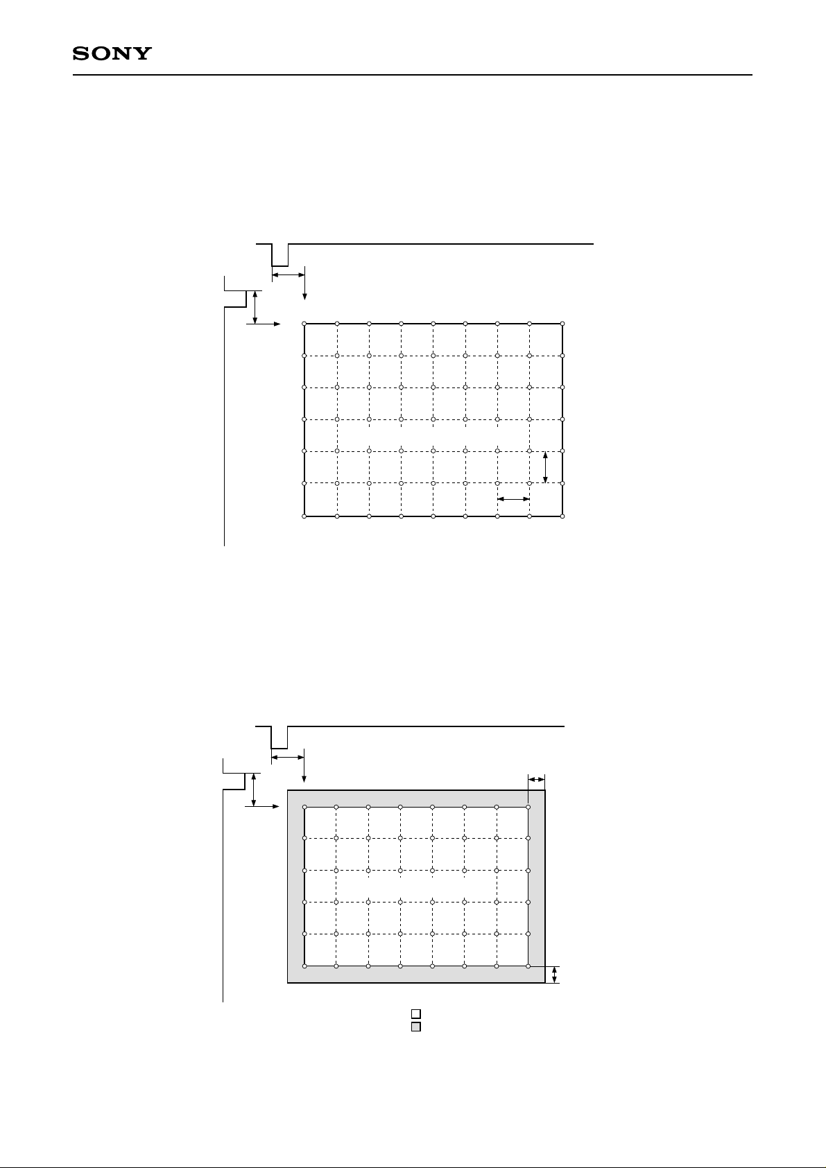
CXD3526GG
(g) CSC_HINT[7:2] and CSC_VINT[7:2] (sub addresses: 3005h and 3006h)
These set the correction interval for the horizontal and vertical directions of the color shading correction block
in 6 bits. This setting has a setting range from 32 to 256 dots (lines) and can be set in 4-dot (-line) units.
Set the "correction interval/4 – 1" value.
HDIN
Number of
correction points
CSC_HNUM
98765432
Correction interval
CSC_HINT
VDIN
1
1
2
3
4
Correction start position
CSC_VP
5
6
7
Number of
correction points
CSC_VNUM
Correction start position
CSC_HP
Color shading correction range
Correction interval
CSC_VINT
(h) CSC_HOS[7:2] and CSC_VOS[7:2] (sub addresses: 3007h and 3008h)
These set the range for which virtual corrections are to be made. The same data as at the edge of the
correction area for color shading correction is assumed for outside the correction area. It is possible to
independently set values from 0 to 256 dots (lines) for the horizontal and vertical directions in 4-dot (-line)
units.
HDIN
VDIN
Correction start position
CSC_VP
Correction start position
CSC_HP
Color shading correction range
– 80 –
Virtual correction range
CSC_HOS
: Area actually corrected
: Area virtually corrected
Virtual correction range
CSC_VOS
Page 81

CXD3526GG
(i) CSC_GNUM [2:0] (sub address: 3009h)
This sets the number of correction points in the gradual direction for color shading correction. It is possible to
set 1 to 8 points. Set the "number of correction points – 1" value.
(j) CSC_RGP1 to 8[9:1], CSC_GGP1 to 8[9:1] and CSC_BGP1 to 8[9:1] (sub addresses: 300Ah to 3024h)
These set the correction points for color shading correction in the gradual direction in 2-gradual units
independently for each R, G and B signal. Registers are set in order of lowest number beginning from 3FFh.
Always keep this order in mind when setting data.
3FFh Same data as Correction Point 1
CSC_R (G, B) GP1
300h
200h
CSC_R (G, B) GP2
CSC_R (G, B) GP3
CSC_R (G, B) GP4
CSC_R (G, B) GP5
CSC_R (G, B) GP6
100h
000h Same data as Correction Point 8
CSC_R (G, B) GP7
CSC_R (G, B) GP8
(k) CSC_RGD1 to 8, CSC_GGD1 to 8 and CSC_BGD1 to 8 (sub addresses: 3025h to 3027h)
These set to expand data set in RAM for color shading correction by ± 8bits by shifting data 1 bit in the MSB
direction. This setting can be made independently for correction points in the gradual direction for each R, G
and B signal.
Setting value: 1 = Expand by ±8 bits; 0 = Not expanded
(l) CSC_XH (sub address: 3000h)
This sets the cross hatch display ON/OFF used during color shading correction.
Setting value: 1 = Display; 0 = Not displayed
(m) CSC_XH_DAT (sub address: 3028h)
This sets the display le vel (gradual level) of the cross hatch pattern used for color shading correction in 2-gradual
units, 9 bits.
– 81 –
Page 82
Pattern Generator Block Register
CXD3526GG
Sub
address
4000h
4001h
4002h
4003h
4004h
4005h
4006h
4007h
4008h
4009h
400Ah
400Bh
400Ch
400Dh
400Eh
400Fh
4010h
4011h
4012h
4013h
DATA7
PG_ON
—
—
—
—
—
—
PG_SIG1G[9:8]
Data
DA TA6 DATA5 DATA4 DATA3 DATA2 DATA1 DATA0
PG_R_ON
—
—
PG_G_ON
—
PG_HST[10:8]
PG_HWST[10:8]
PG_VST[10:8]
PG_VWST[10:8]
—
PG_SIG2G[9:8]
PG_B_ON
PG_STRP_SW
PG_HST[7:0]
PG_HSTP[7:0]
PG_HWST[7:0]
PG_HWSTP[7:0]
PG_VST[7:0]
PG_VSTP[7:0]
PG_VWST[7:0]
PG_VWSTP[7:0]
PG_STEP[7:0]
PG_WIDTH[7:0]
—
PG_SIG1R[7:0]
PG_SIG2R[7:0]
—
PG_R_SEL
—
—
—
—
PG_SIG1R[9:8]
PG_SIG1B[9:8]
PG_PAT[2:0]
PG_G_SEL PG_B_SEL
PG_HSTP[10:8]
PG_HWSTP[10:8]
PG_VSTP[10:8]
PG_VWSTP[10:8]
PG_SIG2R[9:8]
PG_SIG2B[9:8]
PG_STAIR_SW
Initial
value
00h
00h
00h
00h
00h
00h
00h
00h
00h
00h
00h
00h
00h
00h
00h
00h
00h
00h
00h
00h
4014h
4015h
4016h
4017h
PG_SIG1G[7:0]
PG_SIG2G[7:0]
PG_SIG1B[7:0]
PG_SIG2B[7:0]
– 82 –
00h
00h
00h
00h
—: Don't care
Page 83
The detailed setting contents of PG block are described below.
(a) PG_ON (sub address: 4000h)
This sets the test signal output ON/OFF.
Setting value: 1 = Test pattern output mode enabled, 0 = Nor mal signal output
(b) PG_R (G, B)_ON (sub address: 4000h)
These set the test signal level setting ON/OFF.
Setting value: 1 = Various settings enabled, 0 = Output fixed to "0"
(c) PG_PAT[2:0] (sub address: 4000h)
This switches the display pattern within the window area.
Setting value: See the table below.
CXD3526GG
0
1
2
Vertical stripe/diagonal stripe
3
4
5
6
Horizontal ramp/horizontal stair
7
Vertical ramp/vertical stair
Raster
Window
Horizontal stripe
Cross hatch
Dot
(d) PG_R (G, B)_SEL (sub address: 4001h)
These switch the pattern and non-pattern signal levels within the effective area.
Setting value: 1 = Pattern signal level is PG_SIG1R (G, B), 0 = Pattern signal level is PG_SIG2R (G, B)
(e) PG_STRP_SW (sub address: 4001h)
(Valid only when PG_PAT[2:0] = 2h)
This switches between vertical stripe and diagonal str ipe.
Setting value: 1 = Diagonal stripe, 0 = Vertical stripe
(f) PG_STAIR_SW (sub address: 4001h)
(Valid only when PG_PAT[2:0] = 6h or 7h)
This switches between ramp and stair.
Setting value: 1 = Stair, 0 = Ramp
(g) PG_HST[10:0] (sub addresses: 4002h and 4003h)
PG_HSTP[10:0] (sub addresses: 4002h and 4004h)
These set the horizontal effective area in 11 bits. The area can be set in 1-dot units.
– 83 –
Page 84

(h) PG_HWST[10:0] (sub addresses: 4005h and 4006h)
PG_HWSTP[10:0] (sub addresses: 4005h and 4007h)
These set the horizontal window area in 11 bits. The area can be set in 1-dot units.
(i) PG_VST[10:0] (sub addresses: 4008h and 4009h)
PG_VSTP[10:0] (sub addresses: 4008h and 400Ah)
These set the vertical effective area in 11 bits. The area can be set in 1-line units.
(j) PG_VWST[10:0] (sub addresses: 400Bh and 400Ch)
PG_VWSTP[10:0] (sub addresses: 400Bh and 400Dh)
These set the vertical window area in 11 bits. The area can be set in 1-line units.
HDIN
CXD3526GG
VDIN
PG_HST
PG_VST
PG_VWST
PG_VWSTP
PG_VSTP
PG_HWST PG_HSTPPG_HWSTP
Effective area
Window area
(k) PG_STEP[7:0] (sub address: 400Eh)
(Valid for PG_PAT[2:0] = 2h, 3h, 4h and 5h)
This sets the vertical stripe, diagonal stripe, horizontal stripe, cross hatch and dot period in 8 bits. The per iod
can be set in 1-dot units.
(l) PG_WIDTH[7:0] (sub ad dress: 400Fh)
(Valid for PG_PAT[2:0] = 2h, 3h, 4h and 5h)
This sets the vertical stripe, diagonal stripe, horizontal stripe, cross hatch and dot line width in 8 bits. The width
can be set in 1-dot units.
(m) PG_SIG1R (G, B)[9:0] and PG_SIG2R (G, B)[9:0] (sub addresses: 4010h to 4017h)
These set the output signal level inside and outside the pattern area within the effective area in 10 bits. The
level can be set with an accuracy of 1 bit.
– 84 –
Page 85

CXD3526GG
Gamma Correction Block
Set the data for the internal RAM of the gamma correction block by dividing 10-bit gamma correction data with
2 bytes as shown in the figure below. First, set 1-byte data of LSB.
Sub address RAM address
8000h
8001h
8002h
8003h
87FEh
87FFh
MSB LSB
D6 D5 D4 D3 D2 D1 D0
D7
——————
D7 D6 D5 D4 D3
——————
·
·
·
·
·
·
D7 D6 D5 D4 D3 D2 D1 D0
——————
·
·
·
·
·
·
D2 D1 D0
D9 D8
D9 D8
D9 D8
—: Don't care
000h
001h
·
·
·
·
·
·
3FFh
Red Gamma Correction Block Setting Example
Color Shading Correction Block
Set the data for the internal RAM of the color shading correction block by putting in order from the correction
data at the upper left of the Screen 1 (correction start position).
The following is a setting example of 17 hor izontal points × 13 vertical points × 3 gradual points = 663 points.
Sub address RAM address
C000h
C0DCh
C0DDh
C1B9h
C1BAh
C296h
MSB LSB
D7
D6 D5 D4 D3 D2 D1 D0 000h (Upper left)
·
·
·
·
D7 D6 D5 D4 D3 D2 D1 D0
D7 D6 D5 D4 D3 D2 D1 D0
·
·
·
·
D7 D6 D5 D4 D3 D2 D1 D0
D7 D6 D5 D4 D3 D2 D1 D0
·
·
·
·
D7 D6 D5 D4 D3 D2 D1 D0
·
·
·
·
·
·
·
·
·
·
·
·
·
·
·
·
0DCh (Lower right)
0DDh (Upper left)
·
·
·
·
1B9h (Lower right)
1BAh (Upper left)
·
·
·
·
296h (Lower right)
Red Color Shading Correction Block Setting Example
– 85 –
Screen 1
correction data
Screen 2
correction data
Screen 3
correction data
Page 86

CXD3526GG
Notes on Handling
• The power supply and GND patterns have a large effect on undesired radiation on the substrate and
interference to analog circuits, etc.
General precautions are as follows.
• Make the GND pattern as wide as possible. Using a multi-layer substrate and a solid ground is recommended.
• Connect each power supply pin to GND via a ceramic chip capacitor of 0.1µF or more located as close to
each pin as possible.
• Do not use this IC under conditions other than the recommended operating conditions.
• Absolute maximum rating values should not be exceeded even momentarily. Exceeding that ratings may
damage the device, leading to eventual breakdown.
• This IC has a MOS structure which is easily damaged by static electricity, so thorough measures should be
taken to prevent electrostatic discharge.
• Since this IC utilizes a MOS structure, it may latch up due to excessive noise or power surge greater than the
maximum rating of the I/O pins, interface with two power supplies of another circuit, or the order in which
power is supplied to circuits. Make a thorough study of measures against the possibility of latch up before
use.
• When the initialization of this IC is performed at power-on, system clear cancellation is performed after the
supply voltage is set in the range of the recommended operating conditions and stabilized. Keep in mind that
the internal circuit may not be initialized correctly if system clear cancellation is performed before the supply
voltage is set in the range of the recommended operating conditions.
• When designing the substrate, take sufficient care for the surrounding temperature and heat radiation, and
make sure the IC junction temperature does not exceed the maximum value.
• Be sure to make the number of dot clocks input to the CXD3526GG in 1H an even number. Note that if there
is an odd number of dot clocks, the internal phase compensation PLL will not operate properly.
• Be sure to make a thorough evaluation of any items not listed in this data sheet.
– 86 –
Page 87
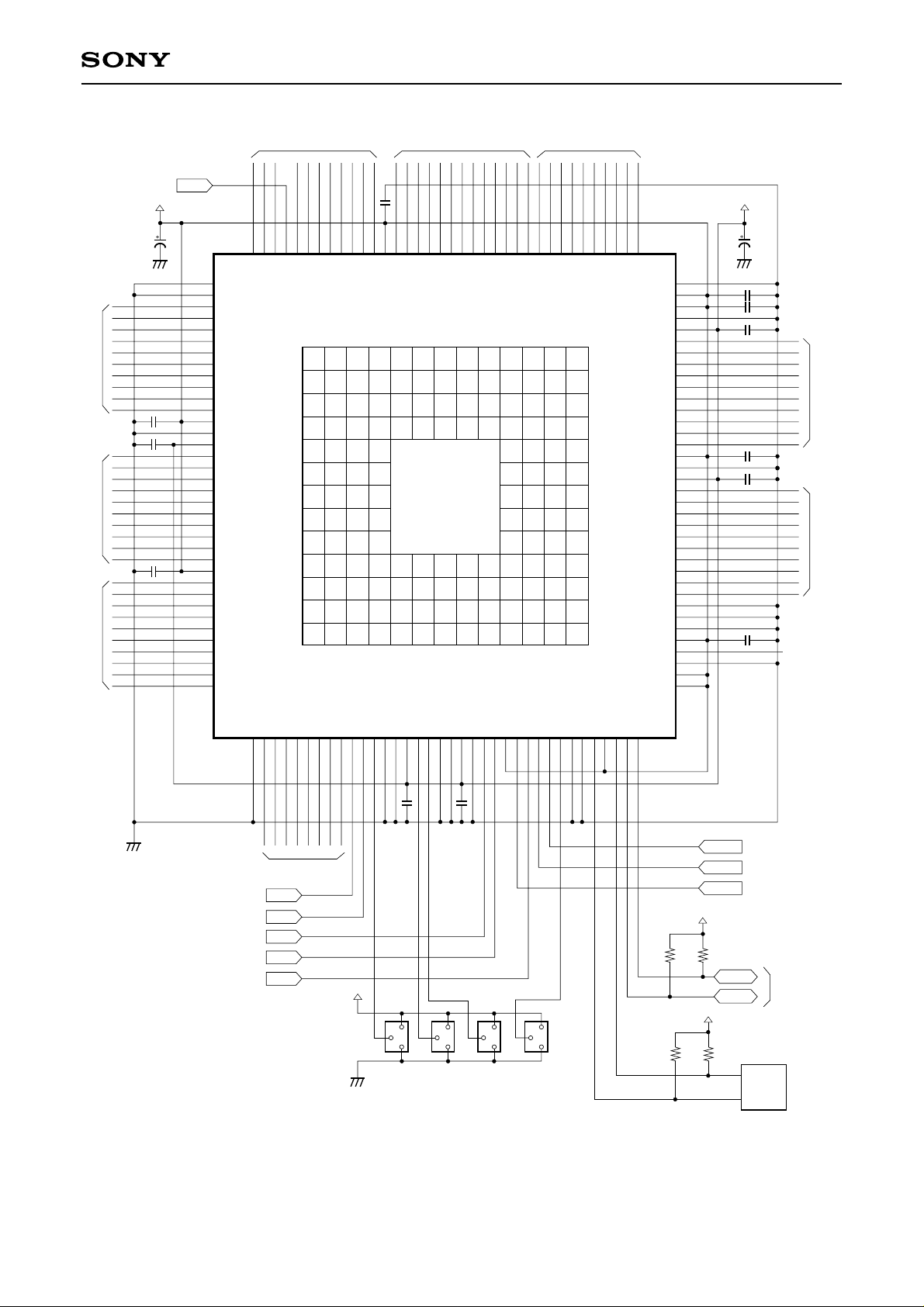
CXD3526GG
Application Circuit
CTRL
+3.3V
10µ
1
85
89
50
90
51
5
91
144
121
122
123
124
125
126
52
5
53
6
92
93
54
7
94
55
8
95
56
9
96
57
10
97
58
11
12
Red inputGreen inputBlue input
0.1µ
0.1µ
0.1µ
2349884748464587
RGT
Vss
Vss
RIN9
RIN8
RIN7
RIN6
RIN5
RIN4
RIN3
RIN2
RIN1
RIN0
V
Vss
V
GIN9
GIN8
GIN7
GIN6
GIN5
GIN4
GIN3
GIN2
GIN1
GIN0
V
BIN9
BIN8
BIN7
BIN6
BIN5
BIN4
BIN3
BIN2
BIN1
BIN0
XRGT
DD2
DD1
DD2
TG output TG output Red output
0.1µ
DWN
PO1
CTRL
PO2
ENB
PRG
1208611944118
DCK1
DCK2
CLR
DD2
V
SHST
14343428384
FRP
HD3
HD2
XFRP
HD1
117
PCG
HCK1
142
HCK2
116
1414182
115383940367980813578113
PST
VST
CLP
HST
VCK
ROUT9
ROUT8
ROUT7
ROUT6
1 484746454443424140393837
2 498887868584838281807936
3 50 89 120 119 118 117 116 115 114 113 78 35
4 51 90 121 144 143 142 141 140 139 112 77 34
5 52 91 122 138 111 76 33
6 53 92 123 137 110 75 32
7 54 93 124 136 109 74 31
8 55 94 125 135 108 73 30
9 56 95 126 134 107 72 29
10 57 96 127 128 129 130 131 132 133 106 71 28
11 58 97 98 99 100 101 102 103 104 105 70 27
12 59 60 61 62 63 64 65 66 67 68 69 26
13 14 15 16 17 18 19 20 21 22 23 24 25
ROUT5
ROUT4
ROUT3
ROUT2
Vss
ROUT1
ROUT0
DD2
V
V
DD2
Vss
DD1
V
GOUT9
GOUT8
GOUT7
GOUT6
GOUT5
GOUT4
GOUT3
GOUT2
GOUT1
GOUT0
V
DD2
Vss
V
DD1
BOUT9
BOUT8
BOUT7
BOUT6
BOUT5
BOUT4
BOUT3
BOUT2
BOUT1
BOUT0
Vss
Vss
Vss
V
DD2
CLKOUT
Vss
TEST4
TEST3
37
114
138
139
140
34
77
112
33
76
111
32
75
110
137
30
31
134
74
109
136
73
108
135
29
72
107
106
71
105
133
132
28
25
27
26
+2.5V
10µ
0.1µ
0.1µ
0.1µ
0.1µ
0.1µ
0.1µ
Clock output
Green outputBlue output
GND
Vss
ROSD0
ROSD1
GOSD0
GOSD1
BOSD0
BOSD1YMYS
HDIN
VDIN
CLKPOL
13145915601661989962176318
OSD input
HDIN
VDIN
TEST1
Vss
127
128
0.1µ
DD1
V
100
CLKSEL
PLLDIV
Vss
641920
129
Vss
0.1µ
DD1
V
21
Vss
CLKP
101
CLKN
TEST5
13065102
XCLR1
CLKC
XCLR2
13166103
XCLR3
HSEL
22
67
TEST6
TEST7
RSCL
2324697068
104
TEST2
RSDA
HSDA
HSCL
XCLR3
XCLR2
XCLR1
+3.3V
CLKP
CLKN
CLKC
+3.3V
3.3k3.3k
HSCL
HSDA
External
CPU
+3.3V
3.3k3.3k
CLKPOL
CLKSEL PLLDIV HSEL
GND
Application circuits shown are typical examples illustrating the operation of the devices. Sony cannot assume responsibility for
any problems arising out of the use of these circuits or for any infringement of third party patent and other right due to same.
External
EEPROM
SCL
SDA
– 87 –
Page 88

Package Outline Unit: mm
CXD3526GG
144PIN BGA
x4
0.2
0.15
AS
12.0
PIN 1 INDEX
0.8
+0.20
1.25
- 0.10
0.38 ± 0.10
0.1
S
S
X
0.2
BS
12.0
0.2
S
DETAIL
SOLDER BALL
A
144-φ0.45 ± 0.01
M
φ0.08
S
AB
X
N
M
L
K
J
H
G
F
E
D
C
B
A
1
SONY CODE
JEITA CODE
JEDEC CODE
PIN 1 INDEX
11
10
9
8765432
1.2
BGA-144P-021
P-BGA144-12X12-0.8
0.8
B
1.2
1312
PACKAGE STRUCTURE
PACKAGE MATERIAL
BOARD MATERIAL
TERMINAL MATERIAL
PACKAGE MASS
EPOXY RESIN
COPPER-CLAD LAMINATE
SOLDER
0.31g
– 88 –
Sony Corporation
 Loading...