

Page 1

CXD3300R
10-bit 20MSPS Video A/D Converter
Description
The CXD3300R is a 10-bit CMOS A/D converter for
video applications. This IC is ideally suited for the
A/D conversion of video signals in TVs, VCRs,
camcorders, etc.
Features
• Resolution: 10 bits ± 1.0LSB (D.L.E.)
• Maximum sampling frequency: 20MSPS
• Low power consumption: 40mW
(Except self-bias )
• Low input capacitance
• Built-in self-bias circuit
Absolute Maximum Ratings (Ta = 25°C)
• Supply voltage AVDD AVSS – 0.5 to +4.5 V
DVDD DVSS – 0.5 to +4.5 V
• Reference voltage VRT, VRB AVDD + 0.5 to AVSS – 0.5 V
• Input voltage VIN AVDD + 0.5 to AVSS – 0.5 V
(analog)
• Input voltage VIH, VIL AVDD + 0.5 to AVSS – 0.5 V
(digital)
• Output voltage VOH, VOL DVDD + 0.5 to DVSS – 0.5 V
(digital)
• Storage temperature Tstg –55 to +150 °C
Recommended Operating Conditions
• Supply voltage AVDD, AVSS 3.0 ± 0.3 V
DVDD, DVSS 3.0 ± 0.3 V
| DVSS – AVSS | 0 to 100 mV
• Reference input voltage VRB 0.3AVDD to 0.5AVDD V
VRT 0.6AVDD to 0.8AVDD V
• Analog input VIN 0.9Vp-p or more
• Clock pulse width tPW1 25 (min.) ns
tPW0 25 (min.) ns
• Operating ambient temperature Topr –40 to +85 °C
– 1 –
E97310-PS
Sony reserves the right to change products and specifications without prior notice. This information does not convey any license by
any implication or otherwise under any patents or other right. Application circuits shown, if any, are typical examples illustrating the
operation of the devices. Sony cannot assume responsibility for any problems arising out of the use of these circuits.
48 pin LQFP (Plastic)
Structure
Silicon gate CMOS IC
Page 2
– 2 –
CXD3300R
A
A
A
A
A
A
A
A
A
A
A
A
A
A
A
A
A
A
A
× 8
DAC
Coarse
Comparate
&
Encode
Calibration
Unit
Fine
Comparate
&
Encode
Fine
Latch
Coarse
Correction
&
Latch
Timing Gen.
2
3
4
5
8
9
10
11
12
15
18
19
20
22
23
24
27
38
42
1
A
Auto
Calibration Pulse
Generator
D9
D8
D7
D6
D5
D4
D3
D2
D1
D0 (LSB)
MINV
LINV
TESTMODE
CAL
RESET
31
VRT
VRTC
VRTS
VRMC
VIN
BE
VRBS
VRB
VRBC
CLK
OE
CE
S/H
Amp
30
36
33
32
28
29
–
+
CE
OE
CLK
AV
DD
MINV
LINV
TESTMODE
AV
DD
AVSS
RESET
TIN
TO
TSTR
VIN
TS
AV
DD
AVSS
CAL
AVDD
AT
AV
DD
AVSS
DVDD
DVSS
BE
AV
DD
AV
SS
VRBS
VRB
VRBC
VRMC
VRTC
VRT
VRTS
AV
DD
AV
SS
D1
D2
D3
D4
DV
SS
DV
DD
D5
D6
D7
D8
D9
D0
2
3
4
5
6
7
8
9
10
11
12
13
14
15
16
17
18
19
20
21
22
23
24
25
26
27
28
29
30
40
39
38
37
36
35
34
31
32
33
41
42
43
44
45
46
47
48
1
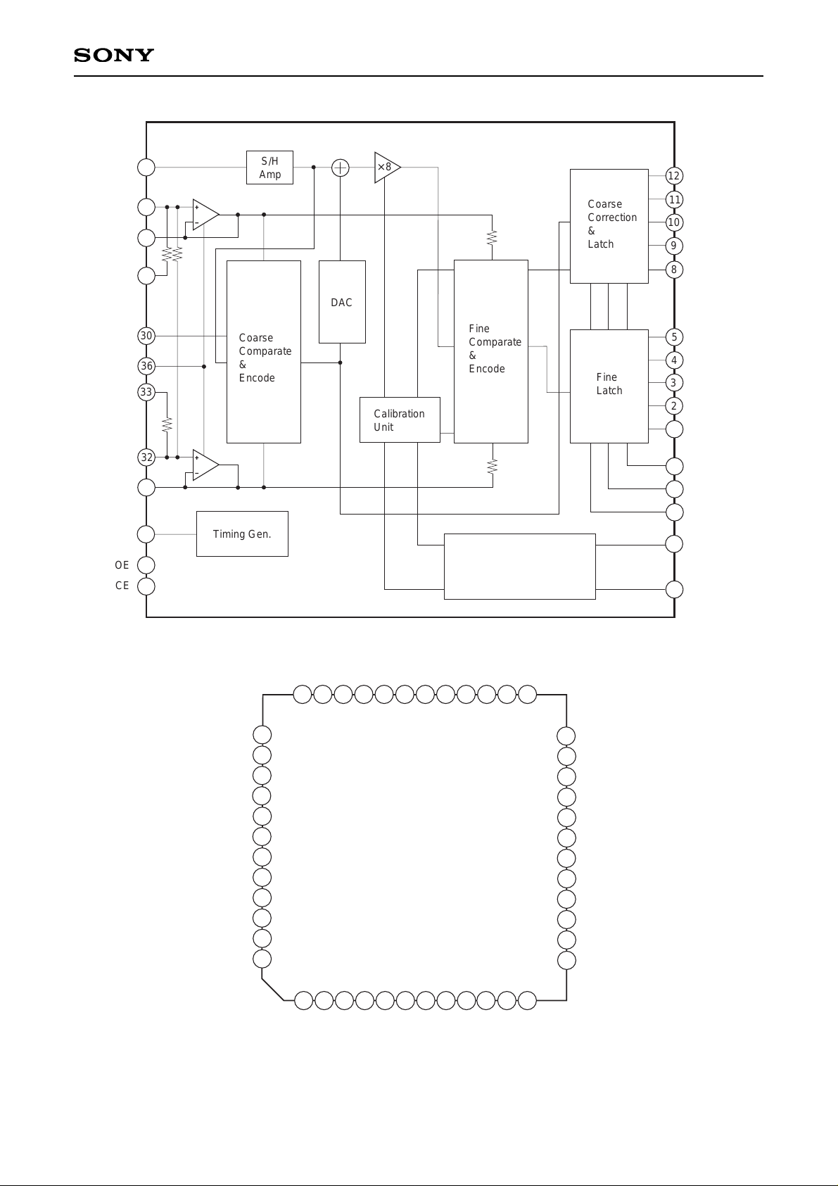
Pin Configuration
Block Diagram
AA
AA
AA
A
A
A
A
A
A
A
A
A
A
A
A
A
AA
AA
AA
AAAA
Page 3
– 3 –
CXD3300R
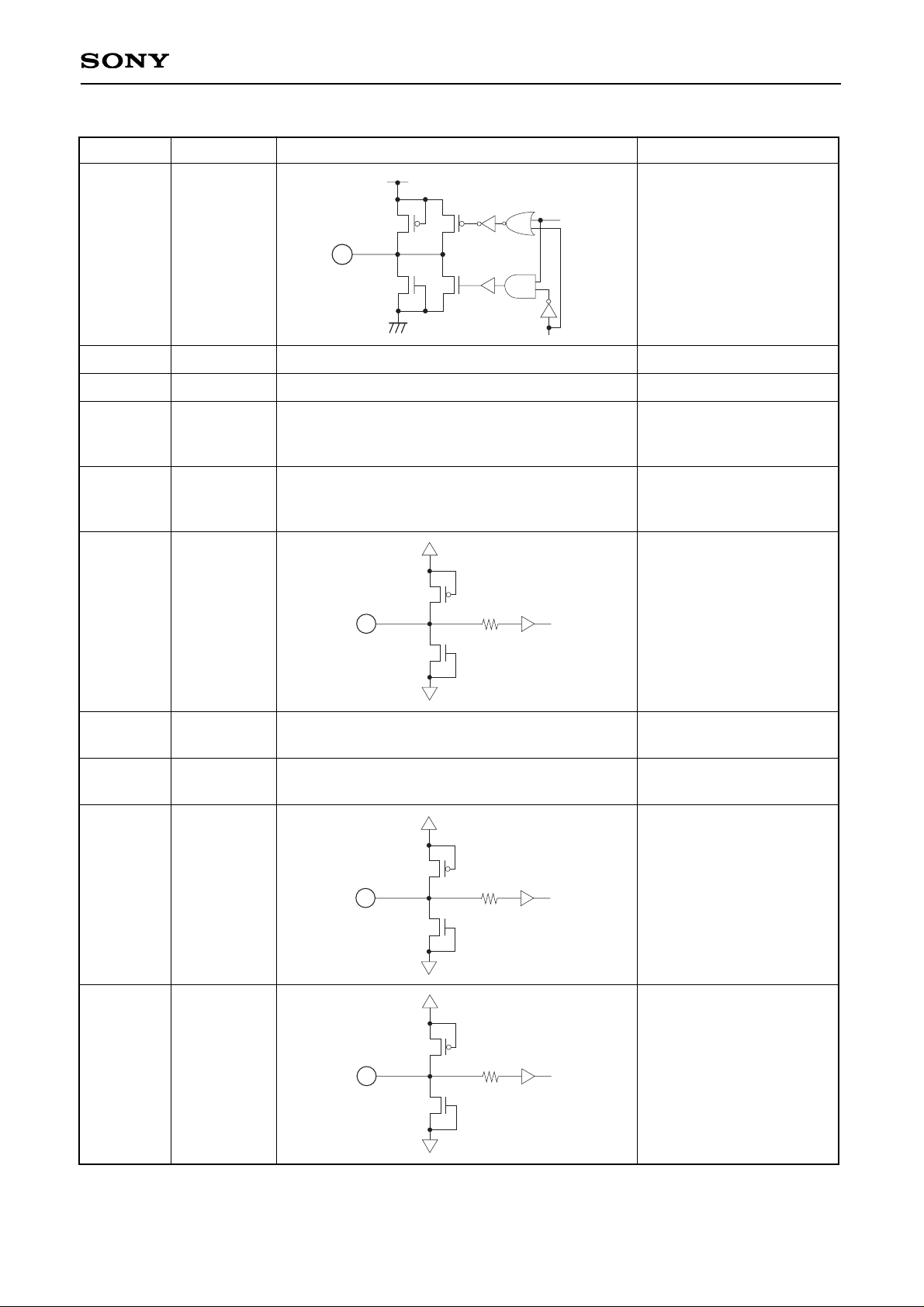
Pin Description
Pin No. Symbol Equivalent circuit Description
1 to 5
8 to 12
D0 to D9
6, 48 DVSS
7, 47 DVDD
13 TO
14 TIN
D0 (LSB) to D9 (MSB)
output.
Digital VSS.
Digital VDD.
Test pin.
High impedance when
TS = High.
Test signal input.
Normally fixed to AVDD or
AVSS.
15 RESET
Calibration circuit reset and
startup calibration restart.
18
TESTMODE
Test mode.
High: Output state
Low: Output fixed
16, 25, 34,
41, 46
AVSS Analog VSS.
17, 21, 26, 35,
40, 43, 45
AVDD
Analog VDD.
DVDD
DVSS
AVDD
AVSS
15
AVDD
AVSS
18
19 LINV
Output inversion.
High: D0 to D8 are
inverted and output.
Low: D0 to D8 are
normal output.
AVDD
AVSS
19
Page 4
– 4 –
CXD3300R
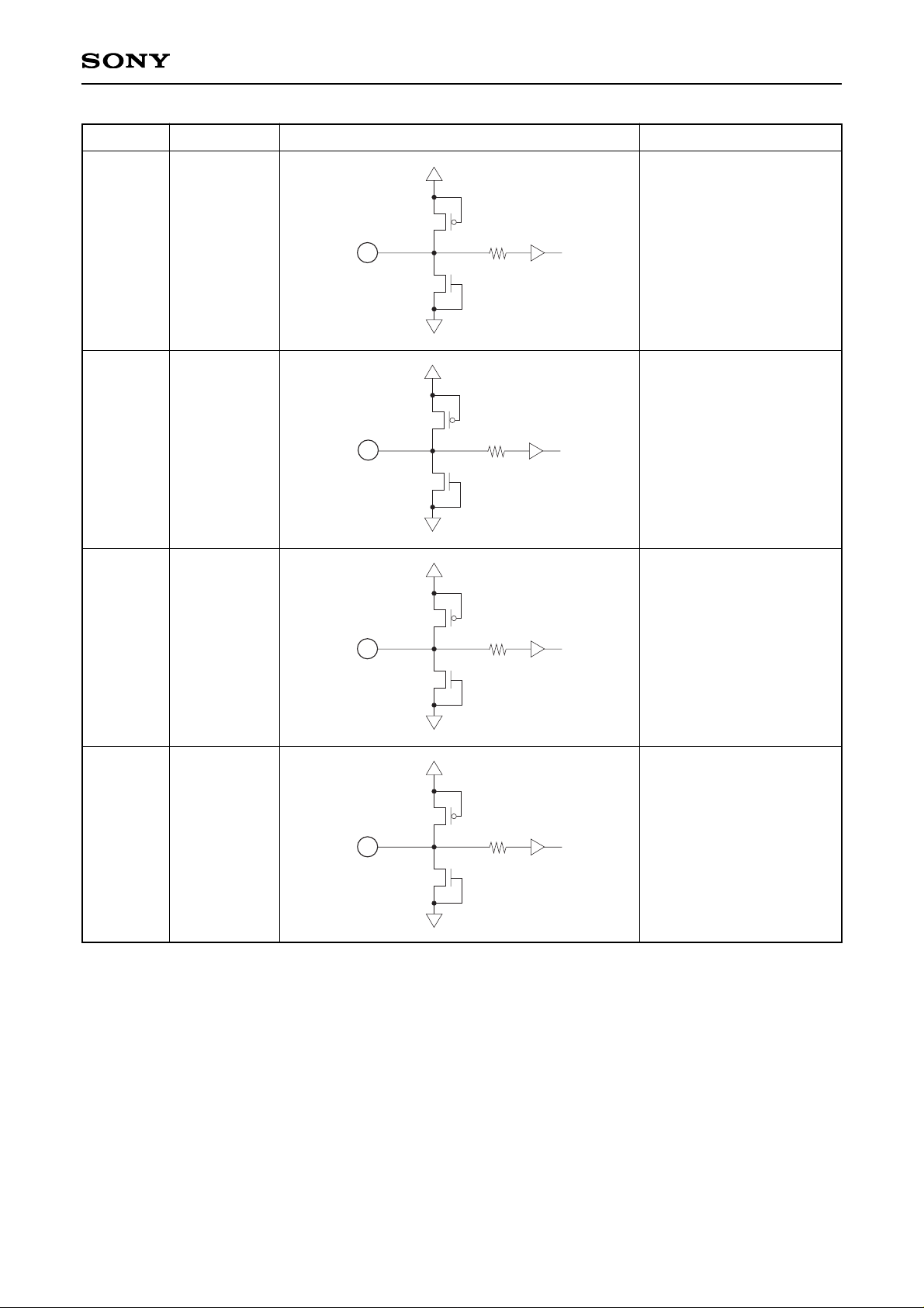
Pin No. Symbol Equivalent circuit Description
20
MINV
Output inversion.
High: D9 is inverted and
output.
Low: D9 is normal output.
AVDD
AVSS
20
22
CLK
Clock.
AVDD
AVSS
22
23
OE
D0 to D9 output enable.
Low: Output state
High: High impedance
state
AVDD
AVSS
23
24
CE
Chip enable.
Low: Active state
High: Standby state
AVDD
AVSS
24
Page 5
– 5 –
CXD3300R
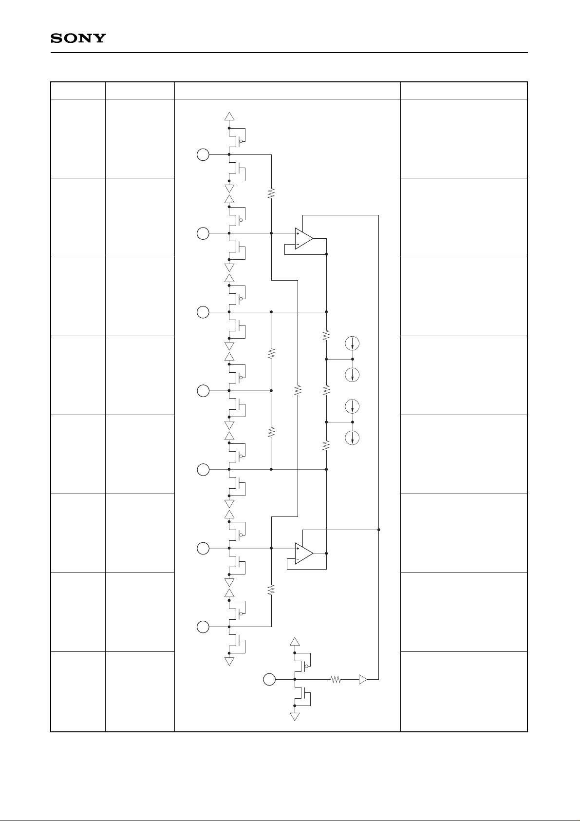
Pin No. Symbol Equivalent circuit Description
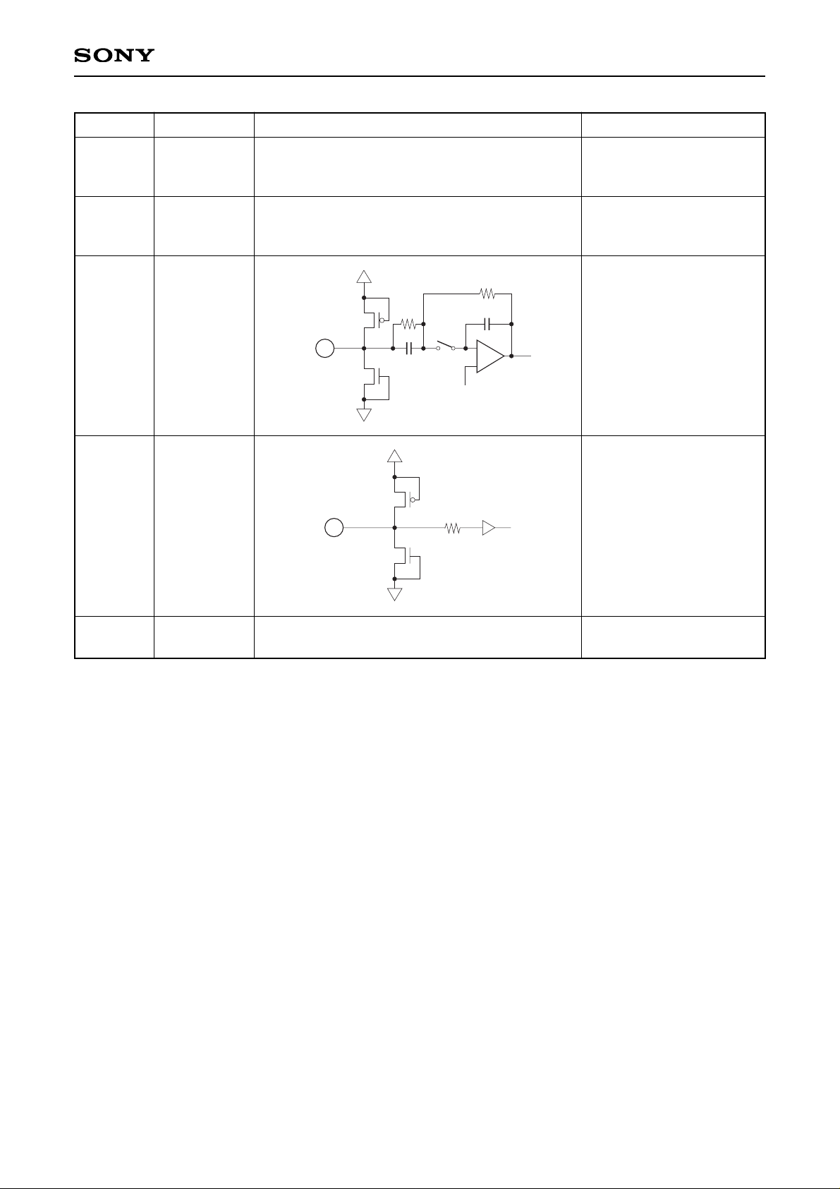
Self-bias.
(Reference top)
27
VRTS
Reference top.
28
VRT
Reference top output.
29 VRTC
Reference middle output.
30 VRMC
Reference bottom output.
31 VRBC
Reference bottom.
32 VRB
Self-bias.
(Reference bottom)
33 VRBS
Bias enable.
36
BE
AVDD
AVSS
AVDD
AVSS
AVDD
AVSS
AVDD
AVSS
AVDD
AVSS
AVDD
AVSS
AVDD
AVSS
AVDD
AVSS
27
28
33
32
29
30
31
36
Page 6
– 6 –
CXD3300R
Pin No. Symbol Equivalent circuit Description
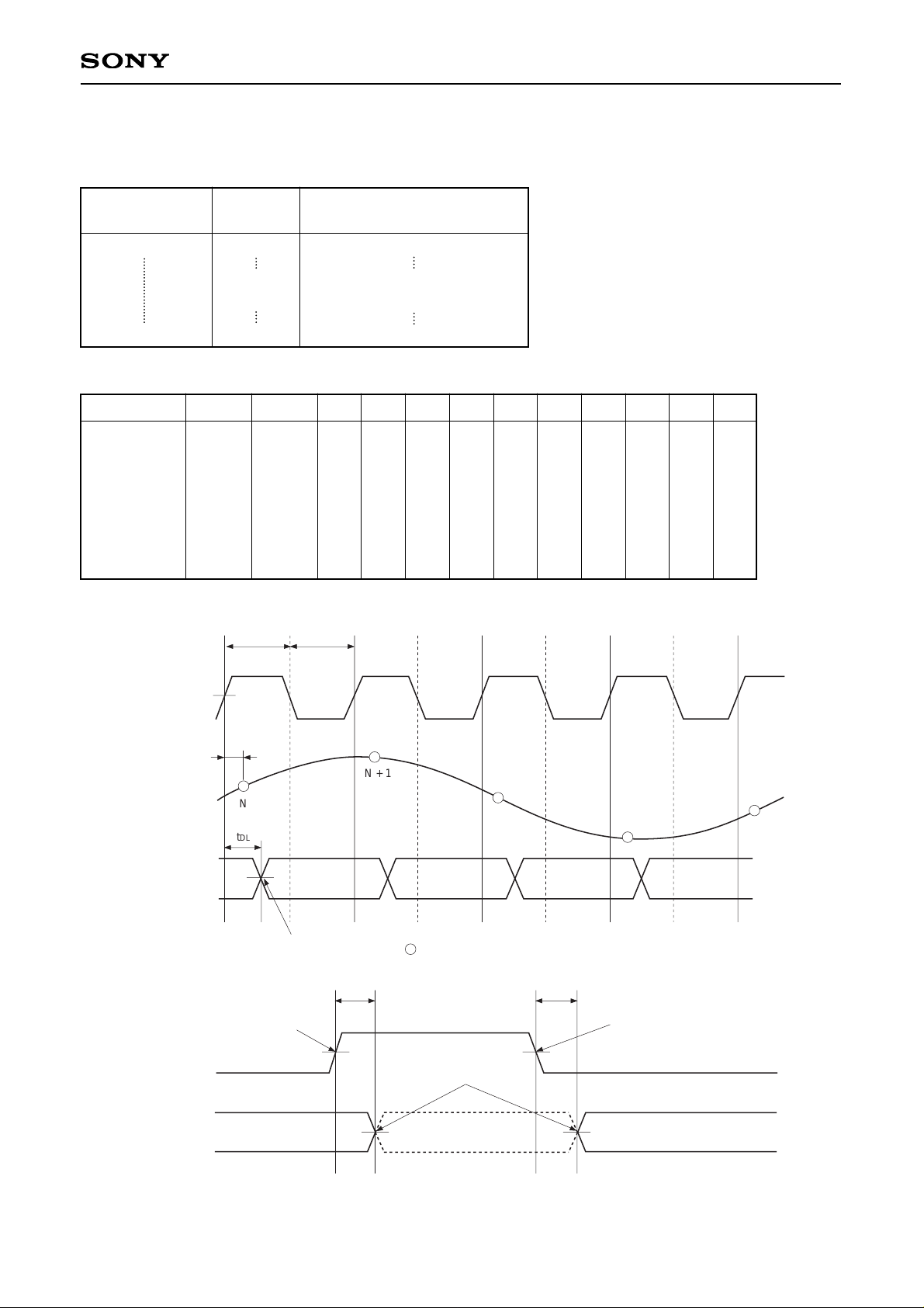
37
TSTR
Test signal input.
Normally fixed to AVDD or
AVSS.
44
AT
Test signal input.
High impedance when
TS = High.
38
VIN
Analog input.
42
CAL
Calibration pulse input.
39
TS
Test signal input.
Normally fixed to AVDD.
AVDD
AVSS
38
AVDD
AVSS
42
Page 7
– 7 –
CXD3300R
tDL
N
N + 1
N + 2
N + 3
N + 4
tPW1 tPW0
: Indicates point at which analog data is sampled
Clock
Analog input
Data output
N – 3 N – 2 NN – 1
1.5V
tSD
1.5V
Digital Output
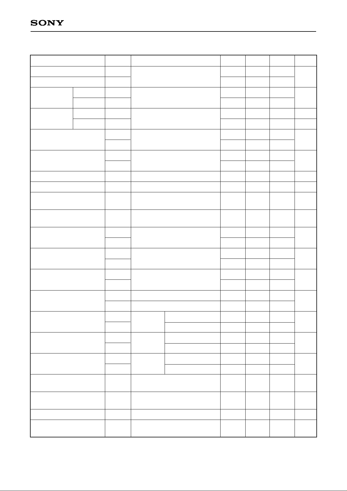
The following table shows the correlation between the analog input voltage and the digital output code.
(TESTMODE = 1, LINV, MINV = 0)
The following table shows the output state for the combination of TESTMODE, LINV, and MINV states.
Input signal
voltage
Digital output code
MSB LSB
VRT
VRB
1111111111
1000000000
0111111111
0000000000
1023
512
511
0
TESTMODE LINV MINV D0 D1 D2 D3 D4 D5 D6 D7 D8 D9
1
1
1
1
0
0
0
0
0
1
0
1
0
1
0
1
0
0
1
1
0
0
1
1
P
N
P
N
1
0
1
0
P
N
P
N
0
1
0
1
P
N
P
N
1
0
1
0
P
N
P
N
1
0
1
0
P
N
P
N
1
0
1
0
P
N
P
N
1
0
1
0
P
P
N
N
0
0
1
1
P
N
P
N
0
1
0
1
P
N
P
N
0
1
0
1
P
N
P
N
0
1
0
1
P: Forward-phase output N: Inverted output
Timing Chart 1
Timing Chart 2
High Impedance
t
PEZ tPZE
Active Active
1.5V
1.5V
Output enable (OE)
Data output
1.5V
Step
Page 8
– 8 –
CXD3300R
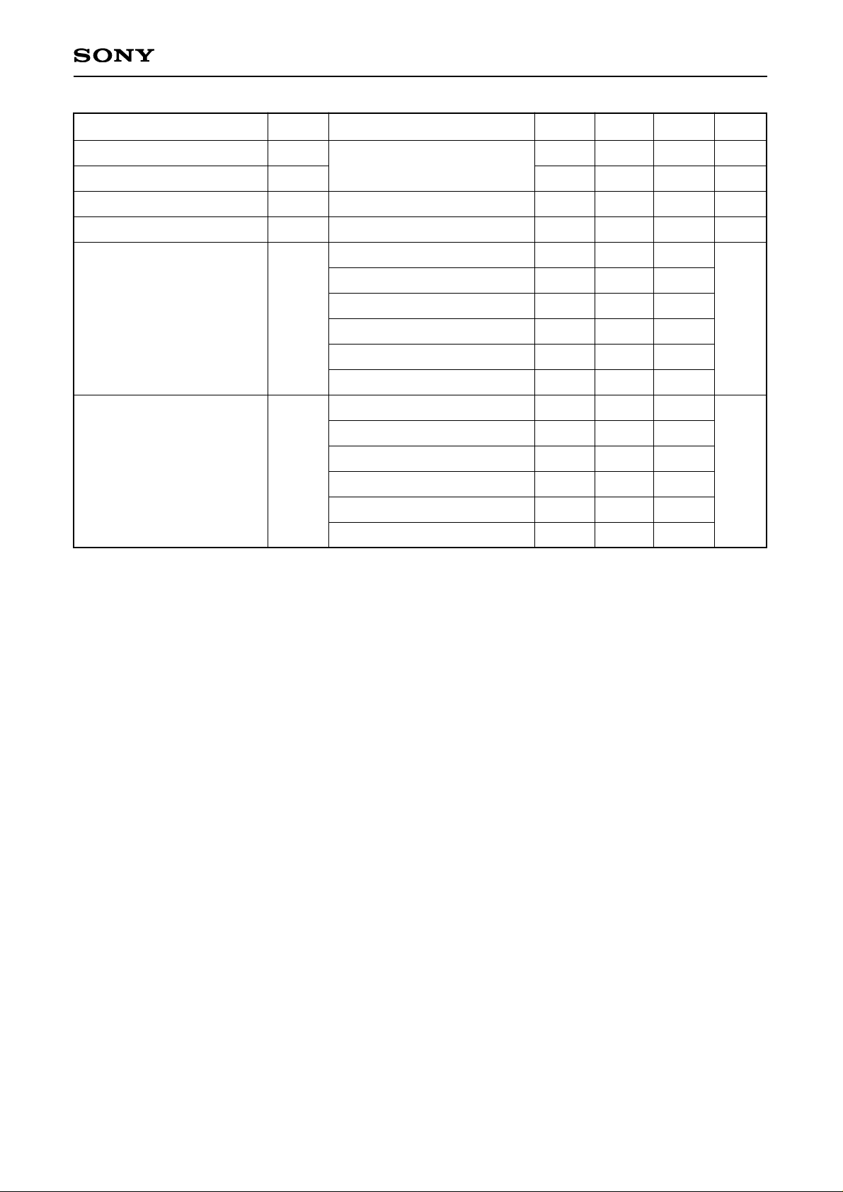
Electrical Characteristics (Fc = 20MSPS, AVDD = 3V, DVDD = 3V, VRB = 1V, VRT = 2V, Ta = 25°C)
Fc max
Fc min
IADD
IDDD
IAST
IDST
IRT1
IRB1
IRT2
IRB2
BW
CIN
RREF1
RREF2
EOT1
EOB1
EOT2
EOB2
VIH
VIL
AIH
AIL
IIH
IIL
IOH
IOL
IOZH
IOZL
tPEZ
tPZE
EL
ED
20
11
87
–111
1.81
–2.33
9k
430
–30
–30
–30
–20
0.7AVDD
40
–55
1.0
1.0
6
3
14
1.0
97
97
2.04
–2.04
85
10
10.3k
490
+5
+5
+5
+10
48
–48
8
5
±1.0
±0.5
0.5
17
4
3.0
1.0
111
–87
2.33
1.81
11.5k
550
+40
+40
+40
+40
0.2AVDD
55
–40
5
5
1
1
10
7
±3.0
±1.0
MSPS
mA
mA
µA
µA
mA
MHz
pF
Ω
Ω
mV
mV
V
µA
µA
mA
µA
ns
ns
LSB
LSB
Maximum conversion rate
Minimum conversion rate
Supply current
Standby
current
Reference pin current 1
Reference pin current 2
Analog input band
Analog input capacitance
Reference resistance
value 1
Reference resistance
value 2
Offset voltage1
Offset voltage2
Digital input voltage
Analog input current
Digital input current
Digital output current
Digital output current
Tri-state output disable
time
Tri-state output enable
time
Integral nonlinearity error
Differential nonlinearity
error
FIN = 1.0kHz sine wave input
FIN = 1.0kHz sine wave input
BE = High
CE = AVDD
VRTS, VRBS: Open
Between VRT and VRB
BE = AVDD
Between VRTC and VRBC
–1dB
Between VRTS and VRT, VRT
and VRB, VRB and VRBS
Between VRTC and VRBC
BE = AVDD
EOT1 = Theoretical value – Measured value
EOB1 = Measured value – Theoretical value
BE = AVSS
EOT2 = Theoretical value – Measured value
EOB2 = Measured value – Theoretical value
AVDD = 2.7 to 3.3V
VIN = 2V
VIN = 1V
VIH = AVDD
AVDD = 3.3V
VIL = AVSS
OE = AVSS
VOH = DVDD – 0.4V
DVDD = 2.7V
VOL = 0.4V
OE = AVDD
VOH = DVDD
DVDD = 3.3V
VOL = 0V
Clock not synchronized for
active → high impedance
Clock not synchronized for
high impedance → active
Item
Symbol Conditions Min. Typ. Max. Unit
Analog
Digital
Analog
Digital
Page 9
– 9 –
CXD3300R
SNR
SFDR
6
6
1.0
0.3
9
7
50
50
50
50
45
44
52
52
52
52
49
50
%
deg
ns
ns
18
8
dB
dB
SNR
SFDR
Item
Symbol Conditions Min. Typ. Max. Unit
FIN = 100kHz
FIN = 500kHz
FIN = 1MHz
FIN = 3MHz
FIN = 7MHz
FIN = 10MHz
FIN = 100kHz
FIN = 500kHz
FIN = 1MHz
FIN = 3MHz
FIN = 7MHz
FIN = 10MHz
Differential gain error
Differential phase error
Output data delay
Sampling delay
NTSC 40 IRE mod
ramp, Fc = 14.3MSPS
CL = 3pF, Ta = –40 to +85°C
DG
DP
tDL
tSD
Page 10

– 10 –
CXD3300R
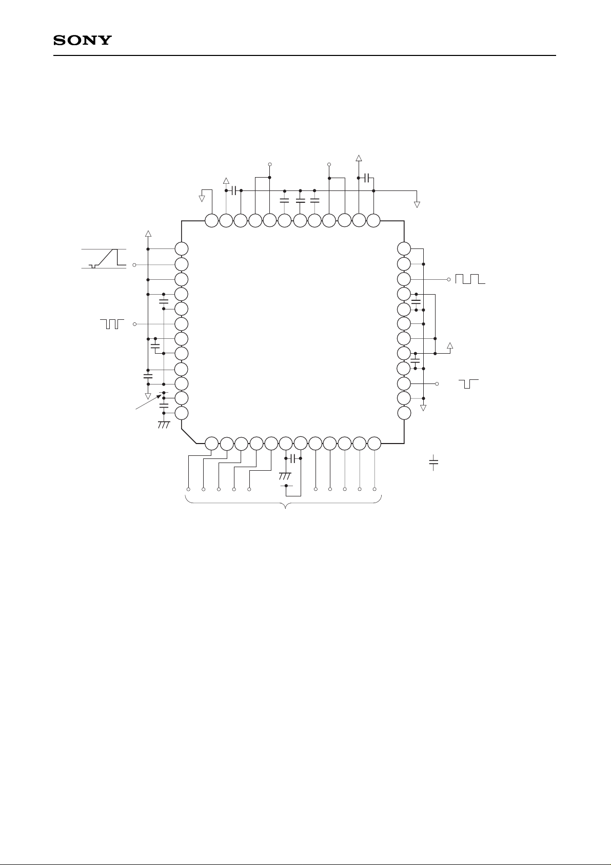
Application Circuit 1
When not using self-bias and the internal bias circuits, and supplying the reference voltage from an external
source.
25
26
27
28
29
30
31
32
33
34
35
36
45
1
2
3
4
5
6
7
8
9
10
11
12
13
14
15
16
17
18
19
20
21
22
23
24
37
39
40
41
42
43
44
47
48
TSTR
VIN
TS
AV
DD
AVSS
CAL
AVDD
AT
AVDD
AVSS
DVDD
DVSS
CE
OE
CLK
AV
DD
MINV
LINV
TESTMODE
AV
DD
AVSS
RESET
TIN
TO
BE
AV
DD
AV
SS
VRBS
VRB
VRBC
VRMC
VRTC
VRT
VRTS
AV
DD
AV
SS
D0
D1
D2
D3
D4
DV
SS
DV
DD
D5
D6
D7
D8
D9
AVDD
AVSS
AVDD
AVSS
: 0.1µF
AV
DD
DVDD
DVSS
AVSS
1V 2V
AV
DD
DVSS
DVDD
46
38
1.0V
2.0V
Clock
input
Digital output
Reset
pulse
Calibration
pulse
Signal input
Application circuits shown are typical examples illustrating the operation of the devices. Sony cannot assume responsibility for
any problems arising out of the use of these circuits or for any infringement of third party patent and other right due to same.
Page 11
– 11 –
CXD3300R
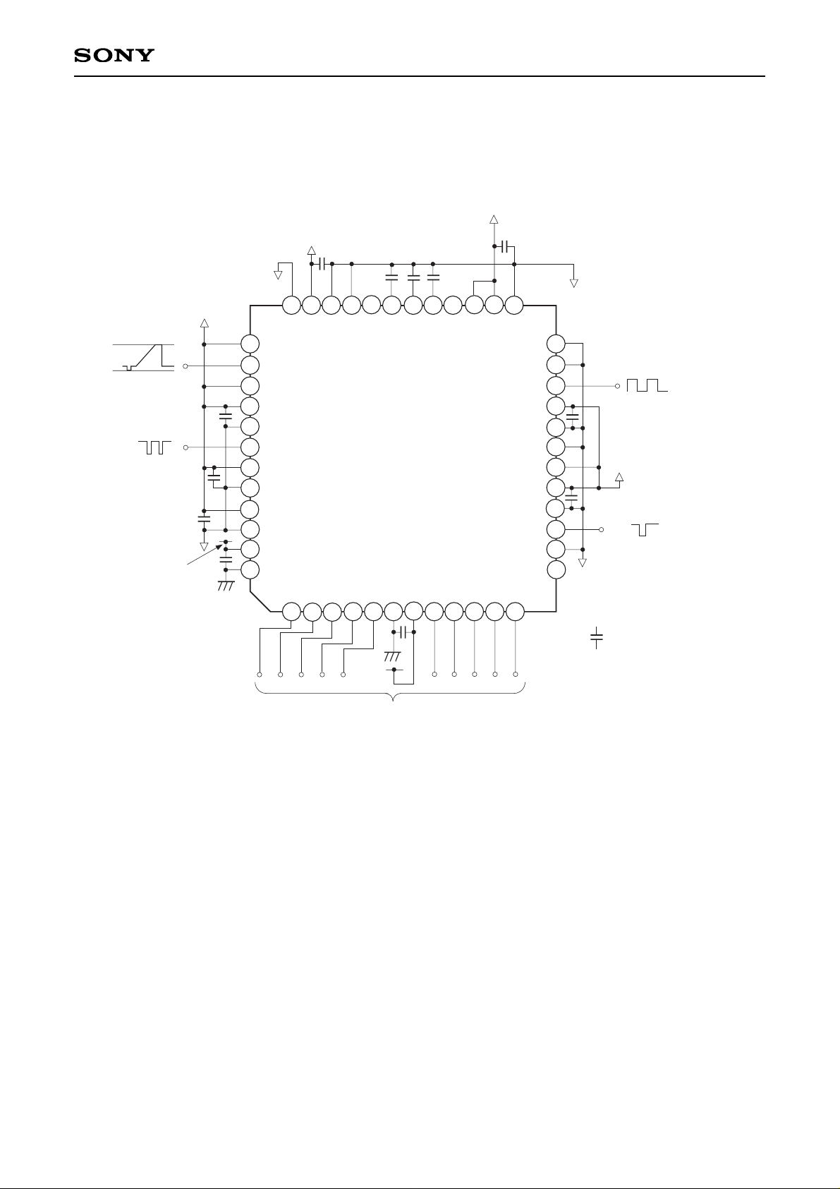
Application Circuit 2
When not using self-bias circuit, using only the internal bias circuit, and supplying the reference voltage from
an external source.
25
26
27
28
29
30
31
32
33
34
35
36
45
1
2
3
4
5
6
7
8
9
10
11
12
13
14
15
16
17
18
19
20
21
22
23
24
37
39
40
41
42
43
44
47
48
TSTR
VIN
TS
AV
DD
AVSS
CAL
AVDD
AT
AVDD
AVSS
DVDD
DVSS
CE
OE
CLK
AV
DD
MINV
LINV
TESTMODE
AV
DD
AVSS
RESET
TIN
TO
BE
AV
DD
AV
SS
VRBS
VRB
VRBC
VRMC
VRTC
VRT
VRTS
AV
DD
AV
SS
D0
D1
D2
D3
D4
DV
SS
DV
DD
D5
D6
D7
D8
D9
AVDD
AVSS
AVDD
AVSS
: 0.1µF
AV
DD
DVDD
DVSS
AVSS
1V
2V
AV
DD
DVSS
DVDD
46
38
1.0V
2.0V
AVSS
Clock
input
Digital output
Reset
pulse
Calibration
pulse
Signal input
Application circuits shown are typical examples illustrating the operation of the devices. Sony cannot assume responsibility for
any problems arising out of the use of these circuits or for any infringement of third party patent and other right due to same.
Page 12
– 12 –
CXD3300R
Application Circuit 3
When using the self-bias and internal bias circuits, and supplying the reference voltage.
25
26
27
28
29
30
31
32
33
34
35
36
45
1
2
3
4
5
6
7
8
9
10
11
12
13
14
15
16
17
18
19
20
21
22
23
24
37
39
40
41
42
43
44
47
48
TSTR
VIN
TS
AV
DD
AVSS
CAL
AVDD
AT
AVDD
AVSS
DVDD
DVSS
CE
OE
CLK
AV
DD
MINV
LINV
TESTMODE
AV
DD
AVSS
RESET
TIN
TO
BE
AV
DD
AV
SS
VRBS
VRB
VRBC
VRMC
VRTC
VRT
VRTS
AV
DD
AV
SS
D0
D1
D2
D3
D4
DV
SS
DV
DD
D5
D6
D7
D8
D9
AVDD
AVSS
AVDD
AVSS
: 0.1µF
AV
DD
DVDD
DVSS
AVSS
AVDD
DVSS
DVDD
46
38
1.0V
2.0V
AVSS
Clock
input
Digital output
Reset
pulse
Calibration
pulse
Signal input
Application circuits shown are typical examples illustrating the operation of the devices. Sony cannot assume responsibility for
any problems arising out of the use of these circuits or for any infringement of third party patent and other right due to same.
Page 13

– 13 –
CXD3300R
1. Calibration function
1) Activating startup calibration
To achieve superior linearity, the CXD3300R has a built-in calibration circuit. When using this IC, therefore,
startup calibration must be activated when the power supply and reference voltage have risen and stabilized.
Care should be taken as only the upper five bits may be output in the worst case if startup calibration is not
activated.
Startup calibration can be activated either at the rise of the RESET pin (Pin 15) or at the fall of the CE pin (Pin
24). The startup calibration activation method for each case is shown in Fig. 1.
a) When using RESET
AV
DD
VRT
VRB
[V]
3
0
[ t ]
RESET
H
L
H
L
33,000 CLK
CE
Startup
calibration
b) When using CE
AV
DD
VRT
VRB
[V]
3
0
[ t ]
RESET
H
L
H
L
33,000 CLK
CE
Startup
calibration
Fig. 1. Startup Calibration Activation Methods
As shown in the figure above, startup calibration must be activated after the supply voltage has risen and
stabilized (full scale of 90% or more). After activation, startup calibration is performed for an interval of about
33,000 clocks. Therefore, care should be taken as the output data during this interval (about 2.3ms at
14.3MHz) cannot be used.
2) Calibration pulse supply
The IC's operating status with changes due to fluctuations in the supply voltage and ambient temperature
during use can be constantly monitored and then compensated appropriately by inputting a pulse at regular
intervals to the CAL pin (Pin 41). Fig. 2 shows the timing chart.
7 clocks
1 clock or more
CLK
CAL
D0 to D9
10ns or more
N – 3
N – 2 N – 1
N
N + 5
Fig. 2. Calibration Timing Chart
Page 14
– 14 –
CXD3300R
[2] Input every V sync
Input
CLK
RESET
CAL
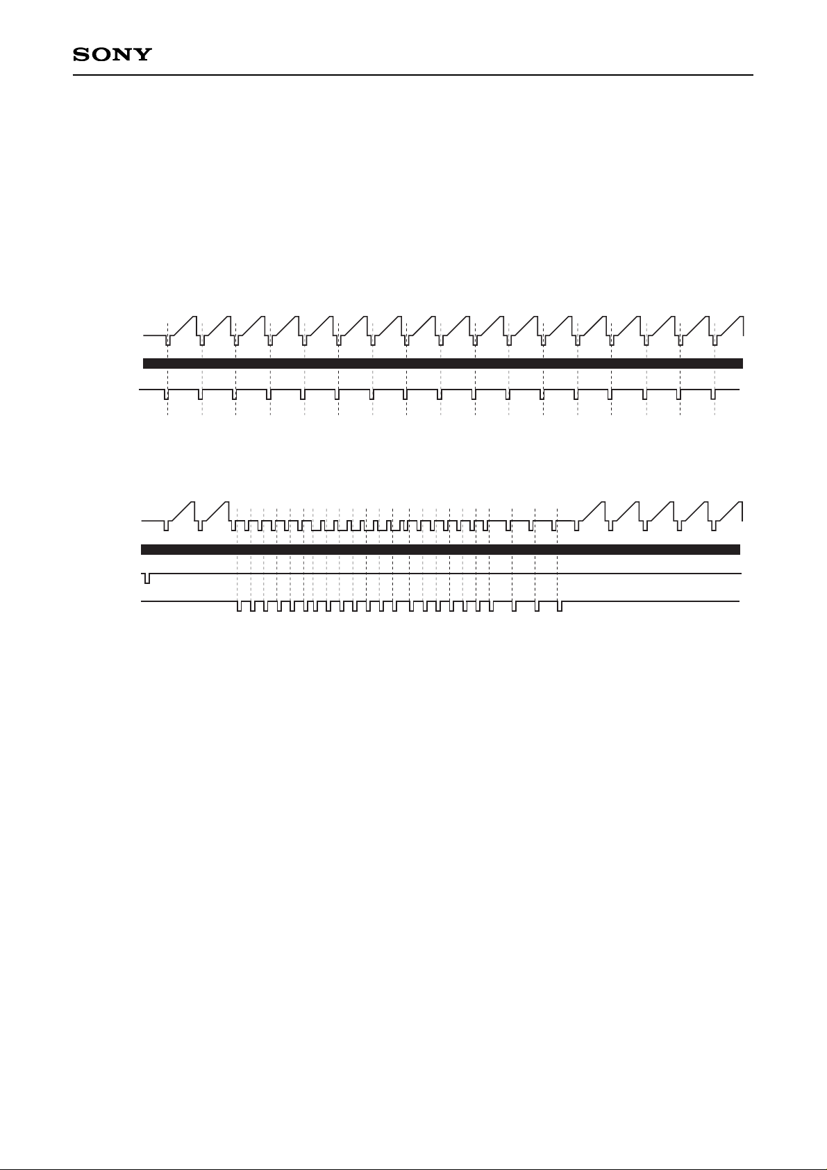
Calibration starts when the fall of the pulse input to the CAL pin (Pin 41) is detected at the clock rise. At this
time, the comparator is used in an exclusive manner for a four clock interval. So, the output data holds the
immediately previous data for a four clock interval after seven clocks from the rise of the clock where the fall of
the calibration pulse was detected, and then the data during this interval is missing.
Therefore, the effects of this function can be avoided by inputting a sync or other signal as the calibration pulse
so that calibration is performed outside of the interval of the actually used video signal. An input example is
shown below.
[1] Input every H sync
Input
CLK
CAL
2. Latch-up
Ensure that the AVDD and DVDD pins share the same power supply on a board to prevent latch-up which may
be caused by power-ON time lag.
3. Board
To obtain full-expected performance from this IC, be sure that the mounting board has a large ground pattern
for lower impedance. It is recommended that the IC be mounted on a board without using a socket to evaluate
its characteristics adequately.
Page 15
– 15 –
CXD3300R
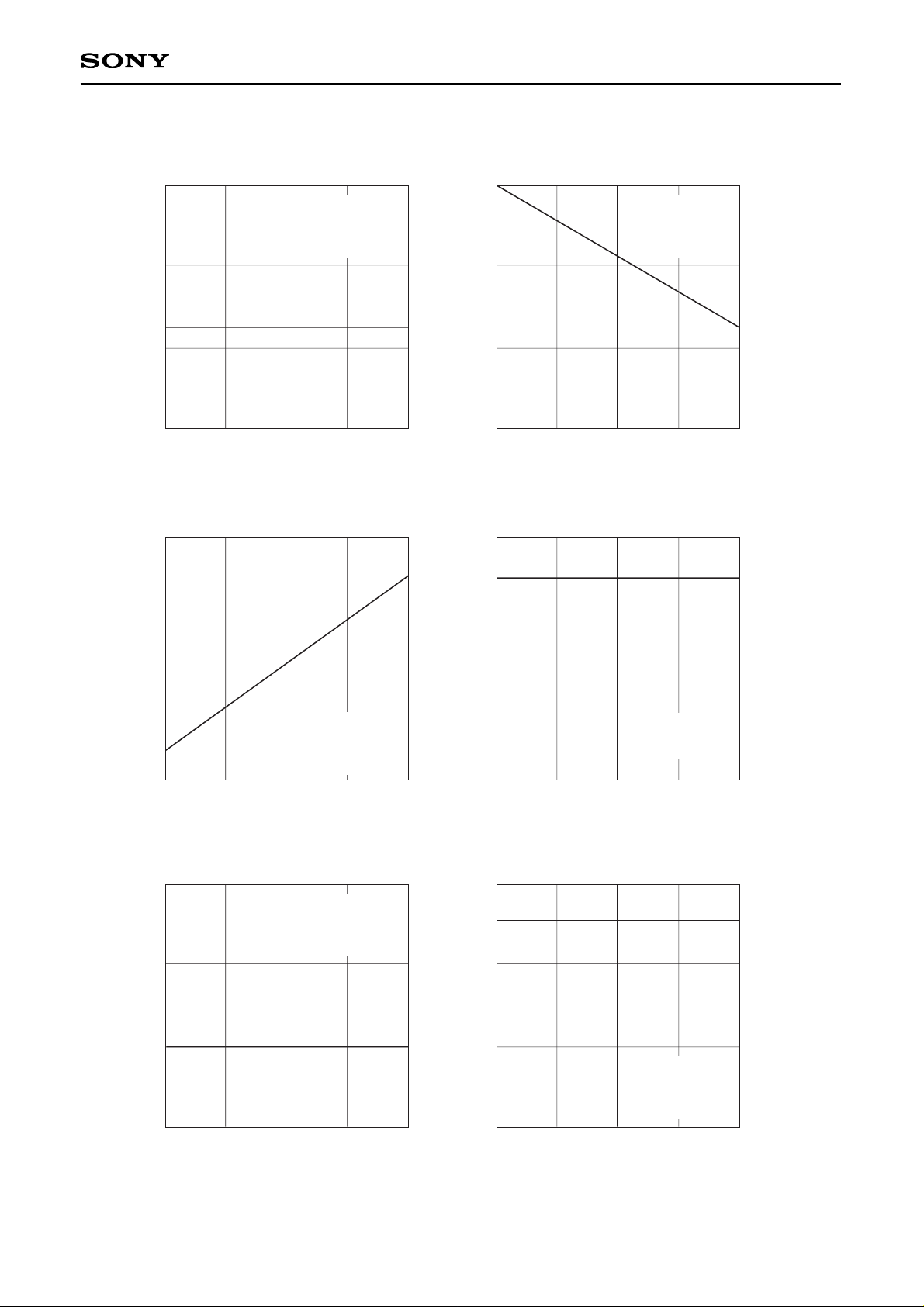
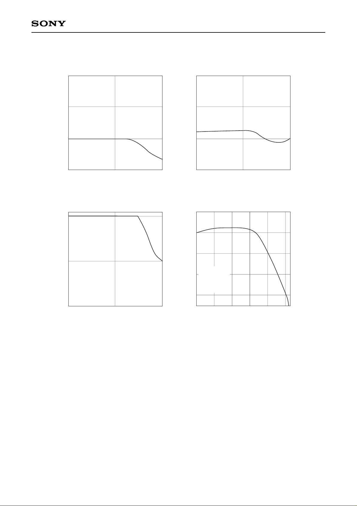
Example of Representative Characteristics
20
18
16
14
–40 0 25 50 85
Ambient temperature [°C]
Supply current [mA]
Supply current vs. Ambient temperature
AVDD = 3.0V
DVDD = 3.0V
Fc = 20MHz
fIN = 1kHz sine wave
38
36
34
32
–40 0 25 50 85
Ambient temperature [°C]
Maximum operating frequency [MHz]
Maximum operating frequency vs.
Ambient temperature
AVDD = 3.0V
DVDD = 3.0V
Fc = 20MHz
fIN = 1kHz sine wave
11
10
9
8
–40 0 25 50 85
Ambient temperature [°C]
Output data delay [ns]
Output data delay vs. Ambient temperature
AVDD = 3.0V
DVDD = 3.0V
Fc = 2MHz
CL = 30pF
8
6
4
2
–40 0 25 50 85
Ambient temperature [°C]
Sampling delay [ns]
Sampling delay vs. Ambient temperature
AVDD = 3.0V
DVDD = 3.0V
Fc = 2MHz
2.0
1.95
1.90
1.85
–40 0 25 50 85
Ambient temperature [°C]
VRTC [V]
VRTC vs. Ambient temperature
AVDD = 3.0V
DVDD = 3.0V
Fc = 20MHz
fIN = 1kHz sine wave
1.20
1.15
1.10
1.05
–40 0 25 50 85
Ambient temperature [°C]
VRBC [V]
VRBC vs. Ambient temperature
AVDD = 3.0V
DVDD = 3.0V
Fc = 20MHz
fIN = 1kHz sine wave
Page 16
– 16 –
CXD3300R
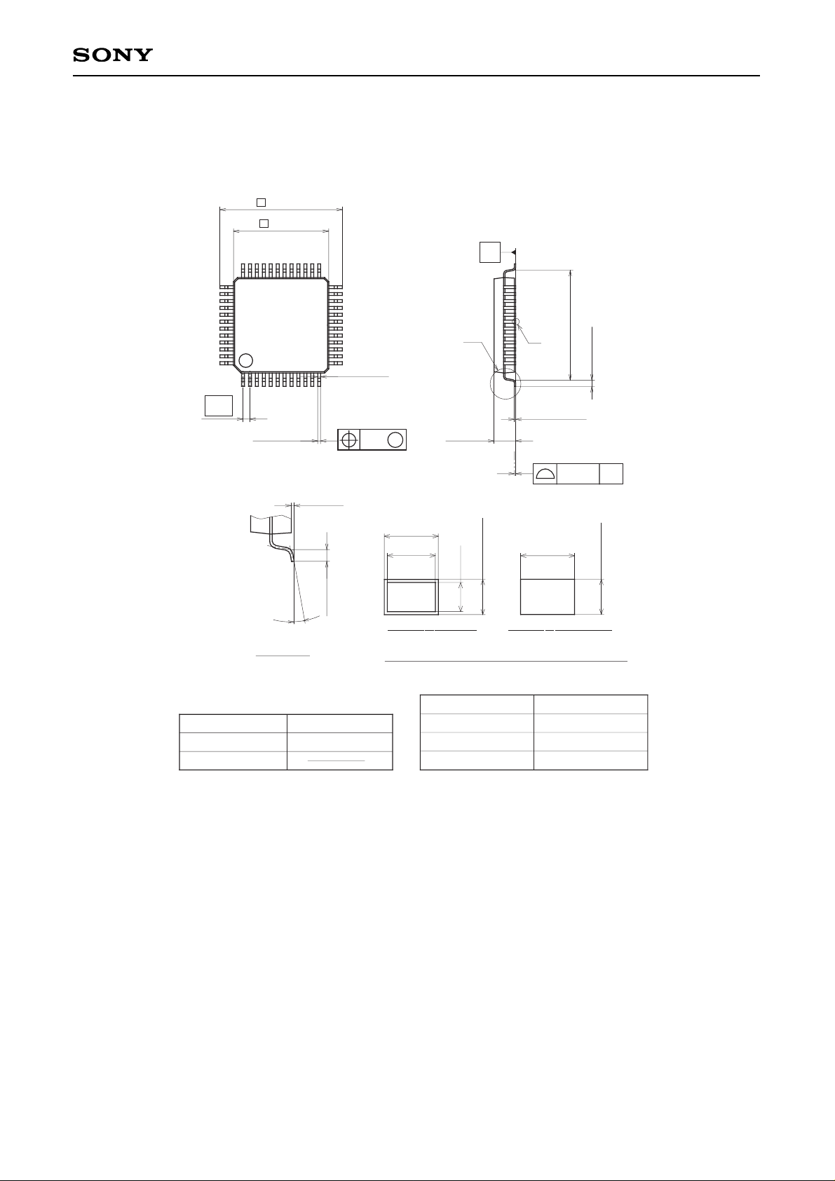
70
60
50
40
100k 1M 100M
Analog input frequency [Hz]
SNR [dB]
SNR vs. Analog input frequency
AVDD = 3.0V
DVDD = 3.0V
Fc = 20MHz
VIN = 1Vp-p
Ta = 25°C
70
60
50
40
100k 1M 100M
Analog input frequency [Hz]
SFDR [dB]
SFDR vs. Analog input frequency
AVDD = 3.0V
DVDD = 3.0V
Fc = 20MHz
VIN = 1Vp-p
Ta = 25°C
8
7
6
100k 1M 100M
Analog input frequency [Hz]
Effective bit [bit]
Effective bit vs. Analog input frequency
AVDD = 3.0V
DVDD = 3.0V
Fc = 20MHz
VIN = 1Vp-p
Ta = 25°C
5M 10M 50M 75M 85M
Analog input frequency [Hz]
Output level [dB]
Analog input band
100M
1
–1
–2
–3
0
AVDD = 3.0V
DVDD = 3.0V
Fc = 20MHz
VIN = 1Vp-p
Ta = 25°C
Page 17
– 17 –
CXD3300R
Package Outline Unit: mm
SONY CODE
EIAJ CODE
JEDEC CODE
PACKAGE MATERIAL
LEAD TREATMENT
LEAD MATERIAL
PACKAGE MASS
EPOXY RESIN
PLATING
42/COPPER ALLOY
PACKAGE STRUCTURE
48PIN LQFP (PLASTIC)
9.0 ± 0.2
∗ 7.0 ± 0.1
1
12
13
24
25
36
37
48
(0.22)
0.18 – 0.03
+ 0.08
0.2g
LQFP-48P-L01
LQFP048-P-0707
(8.0)
0.5 ± 0.2
0.127 – 0.02
+ 0.05
A
1.5 – 0.1
+ 0.2
0.1
SOLDER/PALLADIUM
NOTE: Dimension “∗” does not include mold protrusion.
0.1 ± 0.1
0.5 ± 0.2
0° to 10°
DETAIL A
0.13
M
0.5
S
S
B
DETAIL B:SOLDER
(0.18)
(0.127)
DETAIL B:PALLADIUM
0.127 ± 0.04
0.18 – 0.03
+ 0.08
0.127 – 0.02
+0.05
0.18 ± 0.03
 Loading...